Note: Descriptions are shown in the official language in which they were submitted.
CA 02621103 2014-05-15
54331-10
Nanotube Fabric-Based Sensor Systems and Methods of Making Same
Cross-Reference to Related Applications
[0001] This application claims the benefit under 35 U.S.C. 119(e) of
U.S.
Provisional Patent Application No. 60/714,388, filed September 6, 2005 and
entitled
"Nanotube Fabric Sensor Platform."
[0002] This application is related to the following applications.
U.S. Patent Application No. 10/844,913, now U.S. Patent Publication No.
2005/0053525, filed May 12, 2004 and entitled "Sensor Platform using a
Horizontally
Oriented Nanotube Element;" and
U.S. Patent Application No. 10/844,883, now U.S. Patent Publication No.
2005/0065741, filed May 12, 2004 and entitled "Sensor Platform using a Non-
Horizontally Oriented Nanotube Element."
Background
Technical Field
[0003] The present application relates generally to systems and
methods for the
detection of target analytes, the systems and methods including a nanotube
aspect.
Discussion of Related Art
[0004] Chemical sensors and biosensors have been utilized for
detecting many
species, from contaminants in air (e.g., in air quality sensors) to the
presence of
particular DNA segments in blood samples or other samples. More recently,
chemical
and biosensors utilizing nanotubes, such as single-walled carbon nanotubes
(SWNTs)
have been proposed. See, e.g., J. Kong et al., Science, vol. 287, pp. 622-625
(Jan. 28,
2000)
1
CA 02621103 2014-05-15
54331-10
[0005] Chemical sensors made of nanotubes may be functionalized or
otherwise
modified to become molecule-specific or species-specific sensors. Further
details
may be found in the following references: P. Qi et al., "Toward Large Arrays
of Multiplex
Functionalized Carbon Nanotube Sensors for Highly Sensitive and Selective
Molecular Detection," Nano Lett., vol. 3, no. 3, pp. 347-51 (2003); and Dai et
al.,
"Carbon Nanotube Sensing," U.S. Patent Publication No. 2002/0179434, filed on
June 18, 2002. On the other hand, such sensors may comprise non-functionalized
semiconducting tubes and may sense for the presence of known chemicals, see,
e.g.,
Kong, supra.
[0006] Optical nonlinearity of thin films of nanotubes has been
described, e.g., by
Rashid, et al., "Self-Assembled Organic Supramolecular Thin Films for
Nonlinear
Optics", Organic Electronics 5 (2004) 147-155. Optical nonlinearity is a
feature of some materials
whereby the frequency of light reflected by a material is not equal to the
frequency of
the light that is transmitted onto that material. Lauret, J.-S., et al, "Third-
order optical
nonlinearities of carbon nanotubes in the femtosecond regime", Applied Physics
Letters vol. 85, no. 16 (2004) 3572-2574 have described. Optical
nonlinearities
generally arise in nanotubes due to a change in polarization in the molecular
structure
of the nanotubes from an applied field. Because of the quantum confinement of
the 7t-
electrons associated with their 1-D structure, nanotubes have a large and fast
electronic third-order non-linearity. For further details see Margulis, VI A.,
et al
"Non-degenerate optical four-wave mixing in single-walled carbon nanotubes",
Optics Communications, vol. 249 (2005) 339-349.
Summary
[0007] Some aspects of the present invention provide nanotube fabric-based
sensor systems and
methods of making same. The sensor platforms include nanofabric sensor
elements,
which in some cases include pristine nanotubes and in others include nanotubes
functionalized with analyte-specific molecules. The platforms also include
optical
2
CA 02621103 2008-03-03
WO 2007/030484
PCT/US2006/034627
excitation and detection systems for measuring changes in the non-linear
response of
the nanofabric sensor element arising from an interaction between the element
and
one or more analytes, and from those changes determining the absence or
presence of
the one or more analytes.
[0008] Under one aspect, a system for sensing the presence of an analyte in
a fluid
includes a nanotube sensor element including a plurality of nanotubes and
positioned
for exposure to a fluid; an optical source capable of generating optical
radiation, the
radiation having a source frequency and a fluence selected to generate a
nonlinear
optical response by the nanotube sensor element; an optical detector capable
of
measuring the nonlinear optical response by the nanotube sensor element; and
logic in
electrical communication with the optical detector to sense the presence of an
analyte
in the fluid based on the nonlinear optical response measured by the optical
detector.
[0009] One or more embodiments include one or more of the following
features.
The nanotube sensor element includes a nonwoven fabric of nanotubes. The
nonlinear optical response of the nanotube sensor element includes the
nanotube
sensor element radiating optical energy at a different frequency than the
source
frequency. The nonlinear optical response of the nanotube sensor element
includes
radiation at the third harmonic of the source frequency. Attachment of the
analyte to
the nanotube sensor element changes the nonlinear optical response of the
nanotube
sensor element. Attachment of the analyte to the nanotube sensor element
causes a
charge transfer between the nanotube sensor element and the analyte. The
charge
transfer changes the nonlinear optical response of the nanotube sensor
element. The
logic is capable of determining the change in the nonlinear optical response
of the
nanotube sensor element caused by attachment of the analyte and thus sensing
the
presence of the analyte. The change in the nonlinear response of the nanotube
sensor
element includes a change in frequency of optical energy radiated by the
nanotube
sensor element. The optical detector detects the change in frequency of
optical energy
radiated by the nanotube sensor element. The nanotubes of the nanotube sensor
element include pristine nanotubes. The nanotubes of the nanotube sensor
element
include nanotubes that are functionalized with analyte-specific molecules. The
nanotubes of the nanotube sensor element include nanotubes that are
derivitized with
3
CA 02621103 2008-03-03
WO 2007/030484
PCT/US2006/034627
analyte-specific molecules. The nanotubes of the nanotube sensor element
include
nanotubes that are functionalized with a nonlinear material. The nonlinear
material
causes a change in the nonlinear optical response of the nanotube sensor
element.
The change in the nonlinear optical response includes a change in frequency of
optical
energy radiated by the nanotube sensor element. The nanotubes of the nanotube
sensor element are functionalized so as to have or increase an affinity for a
particular
analyte. The nanotubes of the nanotube sensor element are derivitized so as to
have
or to increase an affinity for a particular analyte. The nanotube sensor
element is
functionalized so as to have or to increase an affinity for multiple analytes.
The
nanotube sensor element is derivitized so as to have or to increase an
affinity for
multiple analytes. The nanotube sensor element includes supports defining a
gap over
which at least a portion of the plurality of nanotubes is suspended. Further
including
material that clamps at least a portion of the plurality of nanotubes to at
least a portion
of the supports. The nanotube sensor element includes a substrate on which the
plurality of nanotubes is disposed. The optical source includes a laser. The
optical
detector includes a photodiode. The nanotube sensor element further includes
nanowires. The system is capable of sensing an analyte selected from the group
consisting of a gaseous element, an airborne molecule, an organic molecule, an
inorganic molecule, and a biological molecule. The biological molecule is
selected
from the group consisting of a peptide, a protein, and a nucleic acid. The
nanotubes
of the nanotube sensor element include substantially a monolayer of nanotubes.
[0010] Under another aspect, a method of using a nanofabric sensor to sense
the
presence of an analyte in a fluid includes characterizing a nanotube sensor
element,
the nanotube sensor element including a plurality of nanotubes, the
characterization
including irradiating the nanotube sensor element with a first optical beam
having a
frequency and a fluence selected to generate a first nonlinear optical
response in the
nanofabric sensor element, and measuring the first nonlinear optical response
of the
nanotube sensor element. The method also includes exposing the nanotube sensor
element to a fluid; and characterizing the nanotube element after fluid
exposure, the
characterization including irradiating the nanotube sensor element with a
second
optical beam having a frequency and a fluence substantially the same as the
frequency
and fluence of the first optical beam to generate a second nonlinear optical
response in
4
CA 02621103 2014-05-15
54331-10
the nanotube sensor element, and measuring the second nonlinear optical
response of the
nanotube sensor element. The method also includes comparing the first and
second nonlinear
optical responses of the nanotube sensor element to sense the presence of an
analyte in the
fluid.
[0011] One or more embodiments include one or more of the following
features. The
nanotube sensor element includes a non-woven fabric of nanotubes. The first
nonlinear
response of the nanotube sensor element is at a different frequency than the
second nonlinear
response of the nanotube sensor element. The frequency of the second nonlinear
response of
the nanotube sensor element is the third harmonic of the first nonlinear
response of the
nanotube sensor element. Further including functionalizing the nanotubes to
have or to
enhance an affinity for the analyte. Further including derivitizing the
nanotubes to have or to
enhance an affinity for the analyte. Further including functionalizing the
nanotubes to have or
to enhance an affinity for a plurality of analytes. Further including
derivitizing the nanotubes
to have or to enhance an affinity for a plurality of analytes. Generating the
radiation with a
laser. The fluid includes a gas. The fluid includes a liquid.
[0011a] According to one aspect of the present invention, there is
provided a system for
sensing the presence of an analyte in a fluid, the system comprising: a
nanotube sensor
element comprising a plurality of nanotubes and positioned for exposure to a
fluid; an optical
source capable of generating optical radiation, the radiation having a source
frequency and a
fluence selected to generate a nonlinear optical response by the nanotube
sensor element; an
optical detector capable of measuring the nonlinear optical response by the
nanotube sensor
element; and logic in electrical communication with the optical detector to
sense the presence
of a first analyte in the fluid based on the nonlinear optical response
measured by the optical
detector wherein the nonlinear optical response comprises the nanotube sensor
element
radiating optical energy at a first frequency before exposure to at least one
analyte inclusive of
the first analyte and the nanotube sensor element radiating optical energy at
a second
frequency after exposure to the first analyte.
[0011b] According to another aspect of the present invention, there is
provided a
method of using a nanofabric sensor to sense the presence of an analyte in a
fluid, the method
5
CA 02621103 2014-05-15
54331-10
comprising: characterizing a nanotube sensor element, the nanotube sensor
element
comprising a plurality of nanotubes, the characterization including:
irradiating the nanotube
sensor element with a first optical beam having a source frequency and a
fluence selected to
generate a second harmonic of the source frequency in the nanofabric sensor
element, and
measuring the second harmonic of the source frequency of the nanotube sensor
element;
exposing the nanotube sensor element to a fluid; characterizing the nanotube
element after
fluid exposure, the characterization including: irradiating the nanotube
sensor element with a
second optical beam having a frequency and a fluence substantially the same as
the source
frequency and fluence of the first optical beam to generate a third harmonic
of the source
1 0 frequency in the nanotube sensor element, and measuring the third
harmonic frequency of the
nanotube sensor element; and comparing the second harmonic frequency and the
third
harmonic of the nanotube sensor element to sense the presence of an analyte in
the fluid.
Brief Description of the Drawings
[0012] In the Drawing,
1 5 Figures IA-C illustrate embodiments of nanosensor systems for
detecting the
presence of analytes at a nanofabric sensor element;
Figures 2A and B are micrographs of exemplary nanotube fabrics;
Figures 3A-C illustrate embodiments of nanofabric sensor elements;
Figures 4A-M and 4L'-M' illustrate structures formed during steps in a method
20 of making horizontally oriented nanofabric sensor
elements;
Figure 5 illustrates a plan view of one possible structure for a large-scale
array
of addressable nanofabric sensor elements;
5a
CA 02621103 2008-03-03
WO 2007/030484
PCT/US2006/034627
Figures 6A and 6B illustrate plan views and cross-sectional views of
embodiments of nanofabric sensor elements; and
Figure 7 illustrates plan views and cross-sectional views of embodiments
of nanofabric sensor elements.
Detailed Description
[0013] Preferred embodiments of the invention provide sensors and sensor
arrays
for biological and/or chemical sensing. They can be built using conventional
semiconductor fabrication techniques and can leverage existing manufacturing
infrastructure and processes to create sensors employing carbon nanotubes. The
manufacturing techniques are largely compatible with CMOS processes and can be
conducted at lower temperatures than those for making conventional nanotube-
based
structures. They allow fabrication of a massive number of sensors on a given
chip or
wafer that can be integrated with various forms of control and computational
circuitry.
[0014] Most embodiments involve utilizing the non-linear optical effects of
carbon nanotube (CNT) fabrics. Electromagnetic radiation interacts with and
generates a non-linear optical response in the CNT fabric (or "nanofabric").
In many
embodiments, the electromagnetic radiation that irradiates the nanofabric has
a
frequency col, and in response the nanofabric emits its own radiation with a
frequency
c02. This process is analogous to harmonic generation, e.g., second harmonic
generation, in which a laser beam at (or centered at) a frequency o)i
irradiates a
material with specified non-linear attributes, which then emits its own light
at a
different frequency w2, e.g., at the second harmonic of the laser beam
frequency. In
general, whenever electromagnetic radiation irradiates the nanofabric, the
fabric
produces radiation of a specific frequency. This radiation is detected by an
optical
detector, such as a photodiode.
[0015] During operation, a chemical or gas may interact with and bind to
the
nanofabric, which can alter the non-linear properties of the nanofabric. These
altered
properties may cause a change in the frequency of the emitted radiation, which
will be
6
CA 02621103 2008-03-03
WO 2007/030484
PCT/US2006/034627
detected by the detector; the change in frequency reflects the presence of
chemicals
and/or gases. For example, if the electromagnetic radiation is at frequency
col, and the
normal nanofabric nonlinear response is at frequency co2, the binding of the
gas or
chemical to the nanofabric may shift the nanofabric's nonlinear response to a
frequency co3. This frequency change thus makes it possible to detect a wide
range of
chemicals and gases.
[0016] Figures 1A through 1B illustrate exemplary nanosensor systems.
Figure
1 A shows a typical set-up to measure the non-linear response of a nanofabric
element
to irradiation. Figure lA illustrates nanosensor system 100 which includes a
light
source 102, e.g., a laser, generated light 104, e.g., a laser beam, nanofabric
sensor
element106, modified light 108 and light detector 110, e.g., a photodiode.
During
operation, light source 102 emits generated light 104, which has a given
frequency col.
Generated light 104 may alternately have a bandwidth that is centered at
frequency col
or otherwise can be characterized by frequency col. Generated light 104
irradiates and
interacts nonlinearly with nanofabric sensor element 106, generating modified
light
108 having frequency (02. Frequency co2 is a different frequency than the
frequency of
the generated light 104, i.e,. 04032. Note that the "conversion" of generated
light 104
to modified light 108 is typically not perfectly efficient, e.g., not 100%, so
some of
the generated light 104 will also simply reflect from nanofabric sensor
element 106,
and will travel in generally the same direction as that of modified light 108.
Detector
110 detects modified light at co2, and may further include optics such as
filters, e.g.,
bandpass or bandblock filters, or polarization optics, to substantially block
residual
generated light 104 and thus enhance the detector's sensitivity to light at
02.
[0017] Figure 1B illustrates a system similar to that shown in Figure 1A,
but in
which a plurality of bound molecules 118 are attached to nanofabric sensor
element
106 . The bound molecules in this example are selected to bind pre-determined
analyte molecules with a high degree of specificity. As discussed in further
detail
below, the plurality of bound molecules 118 may be covalently or otherwise
bound to
the nanotubes in nanofabric sensor element 106. The attachment of bound
molecules
118 to nanofabric sensor element 106 modifies the nonlinear response of
element 106
7
CA 02621103 2008-03-03
WO 2007/030484
PCT/US2006/034627
to generated light 104 at co, such that element 106 generates modified light
115 at
frequency c03, which is different both from col and co2.
[0018] Figure 1C illustrates the system of Figure 1B, but further including
a
analyte species 120 attached to bound molecules 118. Here, the generated light
104
irradiates and interacts nonlinearly with nanofabric 106, to which is bound
the
complex of bound molecules 118 and attached analyte species 120. The
attachment
of complex 118, 120 to nanofabric sensor element 106 modifies the nonlinear
response of nanofabric 106 to generated light 104 at col, such that nanofabric
generates modified light 114 at frequency co3, which is different frequency
than o)i,
02, and c03. Detector 110 detects modified light 114 at least at cozt, and may
include
other optics such as filters or polarization optics to enhance its sensitivity
to this
frequency. Detector 110 may also detect light at eoi, co2, and/or c03. For
example,
modified light 115 at frequency ob, which is generated by nanofabric sensor
element
106 having attached bound molecules 118, could be used as a "control"
condition
which would then allow a later change to the modified light frequency, such as
that
caused by the attachment of analyte 120 to the bound molecules, to be measured
and
thus provide a positive result.
[0019] Various optical excitation can be used to irradiate the nanotube
sensor
element and thus generate a measurable nonlinear response. In many
embodiments,
light source 102 will include a laser that has a frequency (01 and a fluence
that is
capable of sufficiently irradiating the nanotube sensor element so that the
element
generates a nonlinear response to the irradiation. In some embodiments, light
source
102 will include a continuous wave (CW) laser. In other embodiments, light
source
102 will include an ultrafast laser, e.g., a Ti: Sapphire or Nd:YAG laser,
which
operates at a given repetition rate. In general, the higher the laser fluence
at the
nanotube sensor element, the stronger the element's nonlinear response to the
irradiation. An ultrafast laser will typically have a substantially higher
fluence than a
CW laser operating at the same average power and focused to the same spot
size, and
so may cause a nanofabric sensor element to have a stronger nonlinear response
than
it would with excitation by a CW laser.
8
CA 02621103 2014-05-15
54331-10
[0020] Likewise, various optical detection systems can be used to
determine the
change in the nanotube sensor element's nonlinear optical response to optical
excitation. The optical detection system may be selected to appropriately
measure the
nonlinear response that the light source causes the nanofabric sensor element
to
generate. Logic in electrical contact with the optical detector then measures
the
presence of one or more analytes based on the nonlinear optical response
measured by
the optical detection system.
[0021] Although the band gap of CNTs makes them highly responsive to
infrared
radiation in many embodiments, a wide range of radiation wavelengths, e.g.,
from UV
to IR wavelengths, can be used in other embodiments, depending on the desired
output signal.
[0022] Non-linear nanosensors can be readily fabricated by using
standard CMOS
and SOI integration techniques. As for other kinds of nanofabric sensors, such
as
those having an electrical characterization as described in U.S. Patent
Publication
Nos. 2005/0053525 and 2005/0065741, large arrays of sensors can be constructed
to
detect a large amount of species with a low false positive or false negative
detection.
[0023] As will be described in more detail below, preferred
embodiments
elements made from a fabric of nanotubes ("nanofabrics"). Further details of
nanofabrics, nanofabric elements, and methods of making same, may be found in
the
identified patent references, given below. The nanofabric elements may be
unmodified (i.e., "pristine"), derivitized, or functionalized, so that they
may be used to
detect chemical analytes, such as gaseous elements, airborne molecules,
organic and
inorganic molecules. In certain embodiments, the chemical analyte may be a
biological molecule such as peptides, proteins, or nucleic acids. For example,
the
nanofabric may be functionalized, either non-covalently or covalently (e.g.,
by
derivatization) so as to interact specifically with a particular analyte. The
modified or
unmodified analyte-sensitive nanofabrics may be incorporated into a nanosensor
system for detection of the corresponding analyte in a sample. Without wishing
to be
bound by theory, it is believed that charge transfer between the (optionally
functionalized) nanofabric and attached, e.g., adsorbed, analyte molecules
changes the
9
CA 02621103 2014-05-15
54331-10
=
nonlinear response of the nanofabric to generated light. This in turn modifies
the
frequency of light that the nanofabric generates in response to the generated
light,
relative to the frequency of light that would be generated by the nanofabric
alone, or
the fimetionalized nanofabric alone. Preferred embodiments provide methods and
compositions for the detection of target analytes using changes in the
frequency of
light that the nanofabric generates in response to irradiation, upon binding
of the
analytes.
[0024] Other embodiments utilize nonlinear properties of
nanoparticles that are
adhered to the sidewall of the CNTs to produce the desired change in frequency
(optical output properties) of emitted radiation. Nanoparticles that are more
susceptible to second order, fourth-order, etc nonlinearities can be adhered
to the
CNTs to generate a larger range of frequency changes. The CNT fabric has the
added
role of providing a supporting matrix to the nanoparticles which may exhibit
nonlinear behavior. The inclusion of the nonlinear nanoparticles will increase
the
range and sensitivity of the chemicallgaseous detection.
[0025] Figures 2A and B are micrographs of actual
nanofabrics. Figure 2A shows
a nanofabric that is suspended over gaps defined by features in the underlying
substrate. Figure 2B shows a nanofabric that conforms to three-dimensional
features
of the underlying substrate. The fabric thickness, nanotube density,
suspension, and
conformal character can be controlled by altering application parameters,
e.g., as
more fully described in the identified patent references.
[0026] Many nanosensor embodiments are compatible with
protocols that
substantially prevent non-specific binding of non-target analytes. For an
example of
non-specific binding prevention, see Star et al., "Electronic Detection of
Specific
Protein Binding Using Nanotube FET Devices," Nano Lett., vol. 3, no. 4, pp.
459-63
(2003).
[0027] The nanofabric of certain embodiments is formed
from a non-woven fabric
or layer of matted nanotubes (described in more detail below and also
described in the
identified patent references). Under certain embodiments, the fabric is formed
of
single-walled carbon nanotubes (SWNTs), but other embodiments may utilize
multi-
CA 02621103 2014-05-15
54331-10
walled carbon nanotubes (MWNTs) or mixtures of single- and multi-walled carbon
nanotubes or other nanoscopic elements, such as nanowires. The fabric of
certain
embodiments has nanotubes with substantially constant porosity. This porosity
may
be substantially determined by, for example, the number and density of spin
coats,
which commonly also plays a principal role in substantially determining the
capacitance of a particular nanofabric.
[0028] Upon successful completion of the sensing activity, it may be
desirable to
be able to reset a device in the field. In order to accomplish such a reset,
it is possible
that an electrical pulse able to cause removal of a sensed molecule from a
nanofabric
sensor element could be provided to clear or zero the state of the element.
Necessary
voltages could be determined for individual element types specifically or
could be
part of an overall reset pattern which might simultaneously clear all of the
elements
from their states at a particular time. Such a reset feature would allow
elements to
become saturated with analytes but then to be returned to their original state
so that
the device could be reused. Reusability would reduce overall cost and
maintenance
requirements. For further details on reusing nanofabric-based sensors, see
U.S. Pat.
No. 7,780,918, entitled "Sensor Platform Using a Horizontally Oriented
Nanotube Element", filed May 12, 2004.
Exemplary Architectural Sensor Platforms
[0029] Figures 3 A-C illustrate various exemplary architectures of
nanofabric
sensor elements that can be used in the system of Figures 1A-1C. As will be
described in greater detail below, the nanofabric in the element may be
derivatized or
functionalized after fabrication of the platform; in some embodiments, the
derivatization or functionalization of the nanofabric may be incorporated into
intermediate manufacturing steps of forming the nanofabric sensor element. In
Figures 3A-3C, an individual nanofabric sensor element is shown, but, as will
be clear
from the description below, the utilization of well-known semiconductor
manufacturing techniques allows these individual nanofabric sensor elements to
be
fabricated on a massive scale so that a given chip or wafer may have a very
large
number of elements that may be essentially identical to one another. The cells
may be
11
CA 02621103 2014-05-15
54331-10
=
organized into massive arrays, small groups, or individual entities. This part
of the
description focuses on the architecture and basic platform. Subsequent
sections
discuss how the properties of the nanofabric itself may be tailored in
specific ways to
achieve specific desired effects.
10030] Figure 3A illustrates structure 300, which includes
nanofabric layer 302,
supports 304, and gap 306. Manufacture of such a structure is described below
in
reference to Figure 4 et seq., as well as in the identified patent references.
In this
embodiment, the nanofabric is suspended over a gap 306 defmed by supports 304.
[0031] Figure 3B illustrates structure 310, which has a
suspended nanofabric
sensor 302, supports 304, gap 306 and pinning elements 308. Pinning elements
308
firmly attach or clamp the nanofabric element 302 to the supports and may be
made
from many different types of materials. Such materials are chosen from those
compatible with the manufacture of the structure and with the particular
sensing
application desired. Exemplary materials may be found in the identified patent
references.
[0032] Figure 3C illustrates nanofabric sensor element 312.
In this embodiment,
nanofabric element 316 is disposed on support material 314, along with
optional
pinning structures 308. Support material 314, which may also be characterized
as a
pinning structure, may be anything consistent with use as a sensor, including
but not
limited to metals, alloys, ceramics, semiconductors, plastics, glass, etc.
Such a
pinning structure can allow facile electrical connection to the nanofabric as
well as
providing support or clamping of the nanofabric to the underlying structure
314. A
pinning structure would in many cases be conductive, but can be insulating or
conductive, depending on the application.
Techniques for Tailorin,g, Characteristics of Nanofabric Elements
[0033] Many specific methods of preparing the nanofabric
can be envisioned,
depending upon the specific sensing requirements for a particular device.
Tuning
methods of production, and the resulting products, to device requirements can
be
12
CA 02621103 2014-05-15
54331-10
=
performed by using a combination of spin coating and photolithography in
conjunction with fimctionalization or derivatization as described herein.
[0034] Nanofabrics may be created by chemical vapor
deposition (CVD) or by
applying prefabricated nanotubes onto a substrate (e.g., spin coating).
Various
exemplary techniques are described in the identified and published patents and
patent applications identified above.
[0035] In the event that CVD-grown nanotubes are to be
utilized, derivatization or
functionalization of the fabric is straightforward. A CVD-grown nanofabric can
be
derivatized or functionalized in the same fashion as the spin-coated fabric.
Nanotubes
grown by CVD can be doped during the growth process with a limited number of
materials such as boron, silicon, indium, germanium, phosphorous, arsenic,
oxygen,
selenium, and other monatomic species using current technologies. After the
CVD
process has been completed, CVD-grown nanotubes can be easily doped with an
even
wider variety of materials, including many types of molecules ¨ for example,
chemicals, drugs, DNA, RNA, peptides, or proteins.
[0036] The fabrication of nanofabrics by spin coating or
otherwise depositing pre-
formed nanotubes is described in the identified patent references. Such an
approach has advantages over fabrication of nanofabrics by CVD. For example,
lower temperatures may be used for manufacture of the device. This allows more
materials to be used as a potential substrate in conjunction with the
nanofabric
element. In addition, prefabricated nanotubes may be derivatized or
functionalized
with nearly limitless agents before the nanotubes are applied to a substrate.
[0037] Other techniques for forming the nanofabric may be
used as well ¨ e.g.,
aerosol application, dipping, or any other appropriate method.
[0038] Nanofabric sensors may include semiconducting
nanotubes, metallic
nanotubes or both. Investigators have shown that metallic nanotubes may be
separated from semiconducting nanotubes by precipitation. See, e.g., D.
Chattopadhyay et al., "A Route for Bulk Separation of Semiconducting from
Metallic
Single-Walled Carbon Nanotubes,"J. Amer. Chem Soc., vol. 125, pp. 3370-75
(Feb.
13
CA 02621103 2014-05-15
54331-10
=
22, 2003). It is therefore an aspect of certain embodiments of the present
invention to create
nanofabrics of controlled composition (semiconducting vs. metallic) using this
or any
other method of separation. According to one precipitation method, single-
walled
nanotubes are acid-treated and then functionalized non-covalently ¨ e.g., in
octadecylamine and tetrahydrofuran ¨ causing metallic species to precipitate
out of
solution while leaving semiconducting nanotubes in solution. Either of the
separate
lots of nanotubes may be used for nanofabric creation once they are separated
from
one another. Separated nanotubes may be used to create nanofabrics for use as
nanosensors with or without functionalization, and such nanotubes may be used
in
spin-coating applications and other appropriate methods as explained herein
and in
identified references. Furthermore, the relative concentrations of
semiconducting
and metallic nanotubes may be controlled. For example, one may create a fabric
of
approximately 90% semiconducting tubes and 10% metallic nanotubes by mixing a
solution of 100% semiconducting nanotubes with a solution of unseparated
nanotubes
to acquire the desired concentration of each type of nanotube. Solutions of
100%
semiconducting tubes may be mixed with solutions of 100% metallic nanotubes as
well.
[0039] Once formed, the nanofabric can be patterned by
using standard
lithography techniques, as described in the identified and published patent
references. Such lithography techniques allow patterning of nanofabric by
permitting
the controlled definition of a region of fabric for use as a sensor element ¨
for
example, in the form of a nanotube ribbon of substantially predetermined
dimensions.
Exemplary Types ofNanofabric Sensor Elements
[0040] A nanofabric sensor element can include carbon
nanotubes or other highly
robust materials, including nanowires that can operate under extreme
conditions with
no loss of sensitivity. Four general types of nanofabric sensor elements have
been
envisioned, which include:
= pristine nanotubes (i.e., non-fimetionalized nanotubes)
14
CA 02621103 2008-03-03
WO 2007/030484
PCT/US2006/034627
= non-covalently functionalized nanotubes
= covalently derivatized nanotubes
= a hybrid mixture of above.
1. Non-Functionalized, or Pristine, Nanotubes
[0041] A first type of nanofabric sensor element utilizes pristine
nanotubes in the
nanofabric element ¨ that is, the nanotubes are non-functionalized nanotubes.
The
surfaces of the nanotubes will adsorb analytes, which will alter the nonlinear
optical
properties of the resulting complex as compared to the pristine nanotubes
alone.
[0042] Under this approach, nanotubes may adsorb molecules or species onto
their surfaces, resulting in a measurable change in frequency of the generated
light.
2.-4. Functionalized Nanotubes
[0043] Functionalizing of nanotubes may be employed to enhance the fabric's
ability to sense chemical and biological species. The functionalizing agent
may be
molecule specific, allowing for the attachment of specific species onto the
nanotubes,
or the functionalizing material may also be a nonlinear material which
produces its
own unique output frequency.
[0044] Before nanotubes are applied to a surface to create a nanofabric,
they can
be functionalized in solution in order to increase the bonding of the tubes to
a surface
and/or to make possible the bonding of, or interaction with, analytes. Such
functionalized nanotubes can be used to create nanofabric sensor elements,
especially
by patterning the nanofabric into specific shapes.
[0045] Nanotubes may be functionalized in suspension before they are used
to
create a nanofabric, and such functionalized tubes may be stored in bulk
before use.
Such bulk-functionalized nanotubes may be mixed with pristine nanotubes to
generate
a partially functionalized nanofabric. More than one variety of functionalized
nanotube solutions may be combined to generate mixtures of nanotubes to make
mixed-functionalized nanofabrics. This procedure can be repeated to generate
CA 02621103 2014-05-15
54331-10
nanofabrics having as many different species of functionalized nanotubes as is
desired
for sensing. Thus, one could, for example, functionalize a nanotube solution
with
DNA sequences or RNA sequences to sense from a test sample just particular
species
of interest, such as those associated only with a specific virus or with
proteins
associated solely with specific forms of cancer. Some embodiments detect
specific
antigens or major histocompatibility complex (MHC)/antigen complexes from
mixtures of fluids to be tested as an early warning sensor of disease or
infection.
[0046] In other embodiments, nanotubes may be functionalized after
nanotubes
have been applied to a substrate in order to create a nanofabric. In this
case, solution
or gas phase functionalization could proceed before or after patterning the
nanofabrics. This technique would lend itself to multiple spatially-
addressable
functionalization events across a surface. For example, one could envision
using an
inkjet-like process to spray various types of fiinctionalizing agents onto
specific
regions of a substrate. Subsequent steps could be used to apply additional
functional
groups in the same or different regions to make nanofabric sensor elements
with
regionally tailored sensing agents on the same substrate. In this way, many
different
types of analytes could be sensed by a given array, potentially with each cell
sensing
for the presence of a different analyte, when light is systematically
transmitted onto
the various sectors of the array and the light generated by the nonlinear
interaction
between each cell and the transmitted light is detected, and the generated
frequency is
interpreted.
[0047] In yet other embodiments, nanotubes may be functionalized
after sensing
regions are patterned out of the bulk nanofabric. The identified patent
references
include exemplary details on creating and patterning nanofabrics. Upon
completion
of patteming, individual regions can be functionalized to serve as specific
sensors.
Multiple serial functionalizations or mixtures of hinctionalizing agents can
be used to
generate hybrid sensors capable of sensing more than one analyte at a time on
a
patterned nanofabric section or many such sections. This property lends itself
to
automation and use with robotics.
16
CA 02621103 2014-05-15
54331-10
=
[0048] Suitable analytes include organic and inorganic
molecules, including
biomolecules. In a preferred embodiment, the target analyte may be
= an environmental pollutant(s), including pesticides, insecticides,
toxins, etc.;
= a chemical or chemicals, including solvents, polymers, organic
materials, etc.;
= one or more types of therapeutic molecules, including therapeutic and
abused drugs, antibiotics, etc.;
= one or more types of biomolecules, including hormones, cytokines,
proteins, lipids, carbohydrates, cellular membrane antigens and
receptors (neural, hormonal, nutrient, and cell surface receptors) or
their ligands, etc;
= whole cells, including prokaryotic (such as pathogenic bacteria) and
eukaryotic cells, including mammalian tumor cells;
= viruses, including retroviruses, herpes viruses, adenoviruses,
lentiviruses, etc.; and
= spores; etc.
[0049] For example, potential analyte molecules include
nucleic acids,
oligonucleotides, nucleosides, and their grammatical equivalents, as well as
any and
all modifications and analogs thereof, as understood in the art ¨ including,
for
example, amino- or thio-modified nucleosides, and nucleotide molecules with
alternate backbones or containing one or more carboxylic sugars, for example
as
described in the following references: Beaucage et al., Tetrahedron, vol. 49,
no. 10, p. 1925
(1993); and Jenkins et al., Chem. Soc. Rev., pp. 169-176 (1995). Hence, quite
generally,
molecules having at least two nucleotides covalently linked together could be
potential analytes.
Further, the category of potential analytes encompasses both
17
CA 02621103 2008-03-03
WO 2007/030484
PCT/US2006/034627
single-stranded and double-stranded nucleic acids, as well as nucleic acids
containing
portions of both double-stranded and single-stranded sequences. Similarly, a
potential
nucleic-acid analyte could be DNA (including genomic or cDNA), RNA, or a
hybrid,
where the nucleic acid contains any combination of deoxyribo- and ribo-
nucleotides,
and any combination of bases, including uracil, adenine, thymine, cytosine,
guanine,
inosine, xathanine, hypoxathanine, etc. Mimetic compounds for any of the above
might also act as potential analytes. In like fashion, potential analytes
include
proteins, oligopeptides, peptides, and their analogs, including proteins
containing non-
naturally occurring amino acids and amino-acid analogs, and peptidomimetic
structures.
[0050] One skilled in the art will understand that a large number of
analytes may
be detected using various embodiments. Any target analyte for which a binding
ligand, described herein, may be made may be detected using the methods and
articles
of various embodiments.
[0051] Nanoimprint lithography may be used as a method of applying
functionalization agents to discrete portions of nanofabric and thus to create
discrete
nanosensors. Such a method is primarily used for making massive arrays with
sub-
100 nm features. Inkjet printing technology may be used for applying
functionalization agents to discrete portions of a nanofabric to create
separate
nanosensors on a given wafer. Inkjet printing can be used to automate the
functionalization of discrete nanofabric sensor elements, either by applying
functionalization agent to nanofabric sensor elements directly, or by applying
fimctionalized nanotubes to the area where a nanofabric sensor element would
reside
on a substrate. Inkjet printing is a non-impact, dot-matrix printing
technology in
which droplets of ink or, in this case, nanotube solutions are "jetted" from a
small
aperture directly to a specified position on a surface or medium to create an
image.
The light transmitter can then be directed at each of the sensing regions
systematically, i.e. the entire array can be manipulated such that each region
falls
under a light source and nonlinearly generated light can be detected and
analyzed,
then the array (or the light source and detector) can be moved so that a
different
sensor can be analyzed.
18
CA 02621103 2014-05-15
54331-10
[0052] Investigators have described a way of immobilizing proteins at
specific
locations on nanotubes. See I. Baneijee et al., "Location-Specific Biological
Functionalization on Nanotubes: Attachment to Proteins at the Ends of
Nanotubes
Using Au Nanocrystal Masks," Nano Lett., vol. 3, no. 3,
pp. 283-287 (2003). Nanosensors can be
made using proteins immobilized at the ends of nanotubes to sense for
complementary
species. According to this method, nanocrystals of gold are applied to the
sidewalls
of nanotubes, and avidin is adsorbed onto the entire surfaces of the
nanotubes. A
chemical etch procedure is performed to remove the gold nanocrystals and
therefore
also remove the avidin overlying the. gold nanocrystals, leaving only the
avidin
attached to the ends of the nanotubes. Thus certain embodiments fabricate
nanosensors using this procedure and immobilize protein and any other
appropriate
molecule at the ends of nanotubes used in nanosensing cells, articles, and
elements,
such that the bound molecule can be used in a ligand-specific regime.
[0053] The resulting nanofabric sensor elements are generally exposed
to
= analytes, either as a part of a fully or nearly fully exposed system or
as part of an
encapsulated system whereby analytes are introduced in a controlled way. For
example, the nanofabric sensor element of a gas sensor may be fully exposed to
the
air, whereas the nanofabric sensor element of a DNA sensor might be
encapsulated
within a complex microfluidic analyte introduction mechanism. With regard to
the
latter, see PCT publication WO 00/62931, "The Use of Microfluidic systems in
the
Electrochemical Detection of Target Analytes." A fluid
= containing analytes may be introduced to a
sensing chamber by way of microchannels. Optional storage chambers and cell
lysing
chambers may be connected to the system by way of other microchannels. Certain
embodiments thus utilize nanofabric sensor elements along with light
transmission
and detection schemes with such microfluidic systems.
[0054] Nanofabric sensor elements according to certain embodiments
may also be
used as a detector according to the principles disclosed in U.S. Pat. No.
6,361,958 to
Sheih. A microfluidic device may include microchannels that have separated
regions that have
19
CA 02621103 2014-05-15
54331-10
a member of a specific binding pair member such as DNA or RNA bound to porous
polymer beads or structures fabricated into the microchannel. The
microchannels
may be fabricated from plastic and are operatively associated with a fluid-
propelling
component and detector. Thus a nanofabric sensor element and light
transmission and
detection platforms into the system of the '958 patent to Sheih.
[0055] The nanosensors according may also be used for analyte
delivery and
detection in conjunction with the nanofluidic channels described in identified
references.
2. Non-Covalent Funetionalization
[0056] A second type of nanofabric sensor element utilizes a
nanofabric element
in which nanotube surfaces are non-covalently functionalized. This allows for
interaction with a wide variety of cations, anions, metal ions, small
molecules, DNA,
and proteins.
[0057] Non-covalent functionalization takes advantage of non-covalent
bonding
of molecules to the sidewalls of nanotubes with substantial retention of the
chemical
structure of the nanotubes. Nanofabric sensor elements can take advantage of
such
functionalization of nanotubes to increase, or make possible, bonding of
nanotubes to
analyte molecules or atoms. Nanofabrics may be non-covalently functionalized
by
adding pyrenes or other chemicals that are known to bind to nanotubes or
graphite.
For example, 1-pyrenebutanoic acid and succinimidyl ester in organic solvent,
such as
dimethylformamide or methanol, can be used to generate a succinimydyl
functionalized nanotube. This method takes advantage of the pyrenyl group's
interaction with the sidewalls of the nanotubes while generating succinyl
ester groups
that are highly reactive with nucleophilic substitution by primary and
secondary
amines found on the surfaces of most proteins and peptides as well as many
drug and
pro-drug compounds ¨ where a "pro-drug" is, for example, an inactive precursor
of a
drug that is converted into active form in the body by normal metabolic
processes.
This functionalization mechanism is used to immobilize proteins and a wide
variety of
other biomolecules onto the sidewalls of SWNTs and to sense specifically for
molecules that conjugate or bind those immobilized molecules preferentially.
For
CA 02621103 2014-05-15
54331-10
example, streptavidin may be adsorbed onto a nanotube surface in order to be
used in
immunohistochemical sensing. See Chen et al., "Non-covalent Sidewall
Functionalization of Single walled Carbon Nanotubes for Protein
Immobilization," J.
Am. Chem. Soc., vol. 123, pp. 3838-39 (2001). The use of such nanosensors is
compatible with
analyte detection systems where non-specific binding is prevented. See e.g.,
Star et al.,
"Electronic Detection of Specific Protein Binding Using Nanotube FET Devices",
Nano Lett.,
vol. 3, no. 4, pp. 459-63 (2003).
[0058] Many methods are known for non-covalently functionalizing
nanotubes.
See, e.g., the following references: J. Kong et al., "Nanotube
Molecular Wires as Chemical Sensors,"
Science, vol. 287, pp. 622-25 (Jan. 28, 2000); U.S. Patent No. 6,528,020; and
U.S.
Pat. Appl. No. 2002/0172963 to Kelley et al., "DNA-Bridged Carbon Nanotube
Arrays." For example, coating of a nanotube with PMMA (polymethylmethacrylate)
has been shown to sensitize the nanotube to NO2 gas, and gold decoration of a
nanotube has been shown to sensitize it to the presence of a thiol vapor, see
U.S.
Patent No. 6,528,020. In fact, since nanotubes retain similar properties to
graphitic sheets,
nearly any method suitable for non-covalently functionalizing graphite may be
used to
functionalize nanotubes.
3. Covalent Functionalization
[0059] The third type of sensor utilizes a nanofabric element in
which a
covalently derivatized nanotube surface allows any of the interactions above.
[0060] Nanotubes have been functionalized using covalent chemical
bonding
methods ¨ e.g., involving diazonium salts. Further detail may be found in the
following references: J.L. Bahr et al., "Functionalization of Carbon Nanotubes
by
Electrochemical Reduction of Aiy1Diazonium Salts: A Bucicy Paper Electrode,"
J. Am. Chem. Soc., vol. 123, no. 27, pp. 6536-42 (2001); J.L. Bahr et al.,
"Highly
21
CA 02621103 2014-05-15
54331-10
Functionalized Carbon Nanotubes Using in Situ Generated Diazonium Compounds,"
Chem. Mater., vol. 13, no. 11, pp. 3823-24 (2001). Other workers have used
solvent-
free methods such as aniline in isoamyl nitrate. See, e.g., C.A. Dyke et al.,
"Solvent-
Free Functionalization of Carbon Nanotubes," J. Am. Chem. Soc., vol. 125,
no.5, pp. 1156-57 (2003). Still others have used oxidative
processes to functionalize nanotubes in one-pot
reactions, in which reactions occur in a single reaction vessel. See, e.g.,
M.G.C. Kahn
et al., "Solubilization of Oxidized Single-Walled Carbon Nanotubes in Organic
and
Aqueous Solvents through Organic Derivatization," Nano Lett.,
vol. 2, no. 11, pp. 1215-18(2002).
Yet others have covalently bound peptide nucleic acid sequences to single-
walled
carbon nanotubes. See, e.g., K.A. Williams et al., "Carbon nanotubes with DNA
Recognition," Nature, vol. 420, p. 761 (2002) .
[0061] For example, Williams et al., supra, uses an approach to
providing
covalently functionalized nanotubes in which the unique properties of a
nanotubes are
combined with the specific molecular-recognition features of DNA by coupling a
nanotube to peptide nucleic acid (PNA, an uncharged DNA analog) and
hybridizing
these macromolecular wires with complementary DNA. Following this example the
inventors envision that such hybridization will be appropriate for nanofabrics
as well.
This allows the incorporation of DNA-derivatized nanofabrics into larger
electronic
devices by recognition-based assembly, and allows using nanofabrics as probes
in
biological systems by sequence-specific attachment. The technique used to
couple
nanofabrics covalently to PNA involves ultrasonically shortening nanofabric
ropes for
1 hour in a 3:1 mixture of concentrated H2SO4 and HNO3. Subsequent exposure to
1
M HC1 produces abundant carboxyl end-groups. This material is then dispersed
in
dimethylformamide (DMF, 99.5%) and incubated for 30 min in 2 inM 1-ethy1-3-(3-
dimethylaminopropyl)carbodiimide hydrochloride and 5 mM N-hydroxysuccinimide
(NHS) to form nanofabric-bearing NHS esters. PNA adducts are then formed by
reacting this material in DMF for 1 hour with excess PNA (sequence: NH2-Glu¨
GTGCTCATGGTG¨CONH2, where Glu is a glutamate amino-acid residue and the
central block represents nucleic-acid bases). The PNA-derivatized nanofabric
is
22
CA 02621103 2014-05-15
54331-10
transferred to water and dispersed in 0.5% aqueous sodium dodecyl sulphate. To
examine DNA hybridization to this modified nanofabric, fragments of double-
stranded DNA with 12-base-pair, single-stranded "sticky" ends that were
complementary to the PNA sequence were used. These fragments were produced by
cutting double-stranded DNA with restriction enzymes and ligating the products
to
single-stranded oligonucleotides. This sticky DNA was hybridized to the PNA¨
nanofabiic in water, deposited on freshly cleaved mica with 5 mM MgC12. The
surface was rinsed and dried. Atomic-force micrographs of the
DNA/PNA¨nanofabric
hybrids may then be recorded. The antisense properties of this derivatized
complex
may be exploited in biological applications, for example in biosensors.
[0062] These methods allow appreciable and measurable
functionalization of
nanotubes with specific moieties or sensing agents added directly through
covalent
bonding. In effect, the functionalized nanotube becomes a reactive chemical
itself
and further chemistry can be performed to yield such diverse species as
nanotubes
with nanomystals and inorganic compounds. Further details may be found in the
following references: S. Banerjee et al., "Functionalization of Carbon
Nanotubes with a Metal-
Containing Molecular Complex," Nano Lett., vol. 2, no. 1, pp. 49-53 (2002); S.
Banerjee et al., "Synthesis and Characterization of Carbon Nanotube-
Nanocrystal
Heterostructures," Nano Lett., vol. 2, no. 3, pp. 195-200 (2002); S. Banerjee
et al.,
"Structural Characterization, Optical Properties, and Improved Solubility of
Carbon
Nanotubes Functionalized with Willcinson's Catalyst," J. Ain. Chem. Soc., vol.
124,
no. 30, pp. 8490-48 (2002). These functionalized-nanotube building blocks can
be
modified using the wealth of available chemistries to decorate them with
groups and
moieties necessary to sense nearly any chemical or biological agent desired.
[0063] As is the case with non-covalently functionalized, covalently
functionalized nanotubes may be used in three ways to create nanofabric sensor
elements. The nanotubes may be functionalized separately and applied to a
substrate,
for example, by using a spin coating method or other method of application. In
other
embodiments, the nanofabric may be applied to a substrate and subsequently
covalently functionalized before patterning. In yet other embodiments, the
nanofabric
23
CA 02621103 2008-03-03
WO 2007/030484
PCT/US2006/034627
may be functionalized after creation and patterning of the nanofabric. Each of
these
three methods lends itself to creation of a nanofabric comprising one or more
types of
fimctionalized nanotubes in the presence or absence of pristine nanotubes,
depending
upon the sensor application desired. Upon successful generation of a source of
nanotubes containing the proper set of functional moieties, a nanosensor
system can
be fabricated using various methods and light detection schemes can be used
with
such nanosensor fabric elements.
4. Hybrid
[00641 A fourth type of nanofabric sensor element uses a mixture of two or
three
of the previously mentioned types. By using such a mixture, a hybrid
nanofabric
sensor element is created with multiple binding-site types potentially able to
detect
multiple analytes and analyte types. Many different possible compositions of
surface-
functionalized nanotubes can be created before nanotubes are applied to the
substrate,
thereby allowing for a mixture of sensing components which can simultaneously
screen for discrete analytes.
Methods of making exemplary embodiments
[00651 Figures 4A-M illustrate various intermediate structures created
during an
exemplary method of creating exemplary nanofabric sensor elements like those
of
Figure 3A or, with some modification.
[0066] A silicon wafer substrate 402 with an insulating or oxide layer 404
is
provided. Alternatively, the substrate may be made from any material suitable
for use
with lithographic etching and electronics, and the oxide layer can be any
suitable
insulator. The oxide layer 404 has a top surface 404'. A nitride layer 406 (or
any
suitable insulator) is deposited on the surface of intermediate structure 404,
thereby
forming intermediate structure 408 of Figure 4A. A non-limiting example of
nitride
thickness is approximately 20 nin for 0.18 micron ground rule (GR). The
nitride
thickness may vary depending on the ground rule of the desired final product.
The
oxide layer 404 is preferably a few nanometers in thickness, but could be as
much as
1 i_tm thick, or far thicker depending on the ultimate use of the sensor.
24
CA 02621103 2014-05-15
54331-10
[0067] Nitride layer 406 is then patterned and etched to generate
cavities
corresponding in size and shape to gap region 412. Remaining nitride layer 414
is left
in the area around such a cavity, thus forming intermediate structure 416 of
Figure
4B.
[0068] Sacrificial layer 418 is deposited on the surface of
intermediate structure
416, forming intermediate structure 420 of Figure 4C. A non-limiting example
of the
material from which sacrificial layer 418 can be made is polysilicon. However,
any
appropriate material selectively etchable (when necessary) over other
materials of
certain embodiments of the present invention can be used, such as, but not
limited too,
amorphous-Silicon, Al, Mo, Ge, Alumina, Ti, Pd, photoresists, polymers, or any
combination of the above. A non-limiting parameter for the thickness of
sacrificial
layer 418 is that it be on the order of 100 to 200 nm.
[0069] The top surface of intermediate structure 420 is planarized
such that the
surface of the remaining polysilicon layer 422 is substantially level with the
top
surface of remaining nitride layer 414, thus forming intermediate structure
424 of
Figure 4D.
[0070] A nanotube fabric 426 is applied to, or formed on, the surface
of
intermediate structure 424, thus forming intermediate structure 428 of Figure
4E.
Non-limiting methods of applying such a fabric are spin coating, aerosol
application,
dipping, or chemical vapor deposition as described in the references listed
and
identified above.
[0071] Resist layer 430 is applied to the surface of intermediate
structure 428,
forming intermediate structure 432 of Figure 4F.
[0072] As indicated in Figure 4G, a nanotube fabric region 437
(indicated by
dashed lines) larger than gap region 412 (see Figure 4E) is patterned by first
lithographically patterning resist layer 430, forming intermediate structure
434 with
exposed nanofabric portions 436 and patterned resist layer 438. Exposed
nanotube
fabric 436 is then removed, forming intermediate structure 440 of Figure 4H. A
non-
limiting method of patterning the nanotube fabric is by plasma aslaing.
CA 02621103 2008-03-03
WO 2007/030484
PCT/US2006/034627
[0073] Patterned resist layer 438 is removed using any appropriate method,
such
as stripping, forming intermediate structure 442 of Figure 41. Structure 442
has
patterned nanotube fabric 444, corresponding essentially to nanotube fabric
region
437 in Figure 4G.
[0074] Polysilicon layer 446 is deposited over the surface of intermediate
structure 442 to form intermediate structure 448 of Figure 4J. A non-limiting
range
for the thickness of polysilicon layer 446 is between about 20 to 50 nm.
Polysilicon
layer 446 is patterned, for example, by etching to form intermediate structure
452 of
Figure 4K, which has remaining polysilicon layer portion 450 over nanotube
sensor
gap region 412. Remaining polysilicon layer portion 460 is larger than
nanotube
sensor gap region 412 and is the same size or larger than the underlying
patterned
nanotube fabric 444.
[0075] Metal layer 464 is deposited over structure 452, thus forming
intermediate
structure 466. The metal 464 is patterned, e.g. lithographically, (steps not
shown) and
polysilicon 422 and 450 is removed, e.g. by etching thus forming structure 4M.
Metal
layer 464 may be deposited without patterning by any appropriate means
including
sputtering or evaporation.
[0076] In cases where the sensor is to be in an encapsulated space and the
nonlinearly generated light must pass through a translucent or transparent
material,
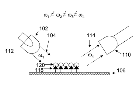
e.g. silicon crystal or ITO, then crystal 464' may be disposed on intermediate
structure 452, thus forming structure 466', as shown in structure 4L'.
Polysilicon
422 and 450 is removed, e.g., by etching, thus forming structure 468 having a
suspended fabric under a crystal covering 464', as shown in structure 4M'.
[0077] The total concentration of binding moieties can be determined by
using
streptavidin that is bound with gold particles. The particles for a given area
of
nanofabric can be counted by SEM or AFM to determine the order of magnitude
sensitivity available within a particular device. Since such derivatization
can take
place over an entire wafer, it is straightforward to fabricate nanofabric
sensor
elements with a very narrow range of characteristic binding concentrations.
26
CA 02621103 2014-05-15
433 1-1 0
[0078] The methods of fabrication for the nanofabric sensor
elements of various
embodiments of the present invention do not require the use of substrates that
can
withstand CVD temperatures. However, such substrates may also be used. Sensors
of preferred embodiments are typically include nanotube fabrics with redundant
conducting nanotubes. These fabrics may be created via CVD, or by room-
temperature operations as described herein and in the identified patent
references.
In such a redundant sensor, if one sensing nanotube breaks, the device would
remain
operable because of the redundant conductive elements in each sensor. Because
the
nanosensor described herein can be fabricated at room temperature, the use of
nearly
any substrate, including highly flexible materials and plastics is possible.
[0079] Nanofabric sensor elements according to certain embodiments
can be
readily manufactured using standard techniques found in the semiconductor
industry
such as spin coating and photolithography. The feature size of each nanofabric
sensor
element can be determined by photolithography or by deposition. Because such
standard techniques are used in the construction of the nanofabric sensor
elements, the
overall cost, yield, and array size can be larger than sensors created by
other known
techniques. Nanofabric sensor elements can also be used in massive parallel
arrays
and can be multiplexed using standard CMOS-compatible sense amplifiers and
control logic.
[0080] Nanofabric sensor elements may also be compatible with high-
resolution
contact printing methods. See H. Li. et al., "High-resolution Printing with
Dendrimers," Nano Lett., vol. 2, no. 4, pp. 347-49(2002).
Patterned nanofabrics may be created on a
substrate (as described below and in the identified patent references), and
those
patterned nanotubes may be transferred via an appropriate contact printing
method to
a second substrate. Parameters such as solubility and binding affinity are
important
factors to be considered in selecting suitable substrates. Alternatively,
ftmctionalized,
patterned nanotubes may be transferred in the same manner. And still another
alternative that utilizes contact printing technology is the application of
patterns of
functionalization agent to specific, defined regions on patterned nanofabric ¨
e.g., on
different nanofabric sensor elements.
27
CA 02621103 2014-05-15
54331-10
[0081] Nanofabric sensor element can be produced on surfaces that can
withstand
CVD temperatures and also on surfaces that may not withstand such a harsh
environment ¨ e.g., when spin coating or aerosol application methods are used
to
create the nanofabric.
[0082] As stated above, the nanotubes of the nanofabric may be
derivatized or
fiuictionalized prior to formation of the nanofabric, subsequent to the
formation of the
fabric, or subsequent to the patterning of the fabric. In the latter case, for
example,
the three-dimensional structure might not be completely sealed but might
instead have
open channels whereby the nanofabric could be subjected to a derivatizing or
functionalizing agent.
[0083] The devices and articles shown and described in the preceding
embodiments are given for illustrative purposes only, and other techniques may
be
used to produce the same or equivalents thereof. Furthermore, the articles
shown may
be modified by the substitution of other types of materials or the use of
different
geometries. For example, as described above, rather than using metallic
electrodes,
some embodiments of the present invention may employ conductive interconnects
made from, or comprising, nanotubes.
[0084] There are other electrode connection locations and geometries
possible
that one skilled in the art would know to create.
[0085] In order to deliver samples to be examined by the sensor, a
microfiuidic
delivery system may be utilized. Samples of blood, body fluids, chemicals, and
the
like may be injected or fed into a microfiuidic delivery system. Such a system
could
then move material through a system of microfluidic capillaries and pumps to
the
sensor site. See, e.g., PCT publication WO 00/62931, "The Use of Microfluidic
systems in the Electrochemical Detection of Target Analytes".
[0086] Some of the advantages of the nanofabric sensor elements
according to
certain embodiments include an ability to implement large-scale application
and
integration. This is facilitated by having CMOS-compatible manufacturing
processes.
28
CA 02621103 2014-05-15
54331-10
Figure 5 illustrates the possibilities for a large-scale array of addressable
nanofabric
sensor elements by showing an array of contact holes in which sensor elements
might
be located.
Figure 6A illustrates a plan view and a cross-sectional view of a nanofabric
sensor
element 814 having a framed portion of nanofabric 802, and a method for its
creation.
Such a framed fabric may be created by providing the nanofabric 802 on a
substrate
804, as illustrated by intermediate structure 800, covering the fabric 802
with an
appropriate covering material 812, as shown illustrated by intermediate
structure 810,
and lithographically patterning and removing a section of the covering
material 812,
leaving a "frame" of material around sensing fabric, as shown in intermediate
structure 820. Such a strapping or clamping method is more fully described in
U.S.
Patent No. 7,259,410, Devices Having Horizontally-Disposed
Nanofabric Articles and Methods of Making Same,
filed February 11, 2004. The covering material may be conductive, and may act
to
alter the electrical properties of the entire patterned fabric, or it may be
semiconducting or insulating. The material of the strapping layer should be
selectively etchable over nanofabric when used alone to open up a window of
exposed
fabric. The material of the covering layer may be selectively etchable over an
intermediate layer disposed between the nanofabric and covering layer. The
intermediate layer in this case may act as an etch stop when etching and
patterning the
covering layer.
[0087] Figure 6B illustrates a plan view and a cross-sectional view
of a nanofabric
sensor element 850 in which no frame is formed, but instead a set of
disconnected
sections of covering layer are formed over a nanotabe fabric 830. Intermediate
structure 810 is patterned to form clamping or pinning structures 842, as
illustrated in
intermediate structure 840.
[0088] Figure 7 illustrates structures formed in yet another method
of patterning
nanofabric sensor elements. Such a method involves a covering material 906
that is
selectively etchable over an intermediate layer 904. Covering material 906 may
preferably be a metal, and intermediate layer 904 may preferably be a
semiconductor
29
CA 02621103 2014-05-15
54331-10 =
¨ e.g., silicon ¨ but any materials suitable for the application will work.
The
intermediate layer 904 is disposed between the nanofabric 802 and covering
layer
906. The intermediate layer 904 in this case may act as an etch stop when dry
etching
and patterning the covering layer 906. Intermediate structure 910 illustrates
patterned
covering layer 912 in the shape of a frame, however any pattern will work
depending
on the requirements of the final product. Intermediate structure 910 is
subjected to an
annealing step whereby covering layer 912 and intermediate layer 904 form a
conducting composite layer 922 ¨ e.g., a metal silicide ¨ permitting creation
of
structure 920. Such a composite layer can act as pinning or clamping structure
or
other contact or addressing element, depending on the use of the final
products.
Other Embodiments
[0089] While the embodiments described above generally relate to
nonlinear
optical effects in which the CNT fabric generates light at a different
frequency (0)z)
than with which it is irradiated (o)i), in general the CNT fabric may have one
or more "
other kinds of nonlinear responses. For example, the CNT fabric may respond to
the
electromagnetic radiation at a)i by shifting or modifying a frequency, phase,
and/or
focusing characteristic of the radiation at col, and this shift or
modification is
measured by an optical detector.
[0090] Besides carbon nanotubes, other materials with nonlinear
optical
properties could be envisioned. As one example, a nanosensing fabric may be
made
entirely of carbon nanotubes, or it may be made from nanowires of various
composition ¨ e.g., silicon nanowires ¨ or the fabric might be a composite of
nanotubes and nanowires. Further details on the creation of nanowires and
composite
fabrics may be found in the identified patent references, such as in U.S. Pat.
No. 7,416,993, entitled "Patterned Nanoscopic Articles and Methods of Making
the Same."
[0091] Fluid samples delivered to a sensor element for analyte
detection can
include both liquids and gases, and may include analytes in a variety of forms
¨ for
example, as part of particulate matter suspended in the fluid.
CA 02621103 2014-05-15
54331-10
[0092] Further, certain of the above aspects, such as the hybrid
circuits, are
applicable to individual nanotubes (e.g., using directed growth techniques,
etc.) or to
nanotube ribbons. As used herein, phrases such as "collection of
nanostructures" or
"collection of nanotubes" each generally encompass a number of nanostructures
or
nanotubes, respectively, and potentially other matter, without regard to such
considerations as whether any particular constituent or constituents of the
collection
have a special quality or distinctiveness, or are arranged in a particular
way.
[0093] The term "functionalization," as used herein, generally
includes both
covalent and non-covalent modifications of nanotubes whereas the term
"derivatization" signifies the covalent modification of nanotubes. Hence,
funetionalization may in certain instances involve non-covalent transformation
of the
surface of a nanotube into a form with different functional groups or
moieties, and, for
example, is meant to encompass any alteration, or addition, to a nanotube or
nanotube
surface ¨ including covalent derivatization ¨ that creates a product with
different
physical or electrical characteristics. Derivatization is indicative of a
covalent
alteration of the chemical structure of one or more nanotubes, or a portion
thereof. In
both circumstances, the process can be controlled such that electrical
properties of
nanotubes may be substantially retained. Functional groups can include
inorganic
atoms and molecules as well as organic molecules. Significant biological
functional
groups include peptides, nucleic acids, antigens (including polypeptide and
non-
polypeptide antigens) as well as peptide nucleic acids.
[0094] The following commonly-owned patent references, referred to
herein as
"identified patent references," describe various techniques for creating
nanotube
elements (nanotube fabric articles and switches), e.g., creating and
patterning
nanotubc fabrics:
U.S. Patent Application No. 09/915,093, Electromechanical Memoly Array
Using Nanotube Ribbons and:Method for Making Sante, filed July 25, 2001,
now U.S. Pat. NO. 6,919,592;
31
CA 02621103 2014-05-15
54331-10
=
U.S. Patent Application No. 09/915,173, Electromechanical Memory Having
Cell Selection Circuitry Constructed with Nanotube Technology, filed July 25,
2001, now U.S. Patent No. 6,643,165;
U.S. Patent Application No. 09/915,095, Hybrid Circuit Having Nanotube
Electromechanical Me11101y, filed July 25, 2001, now U.S. Patent No.
6,574,130;
U.S. Patent Application No. 10/033,323, Electromechanical Three-Trace
Junction Devices, filed December 28, 2001 now U.S. Pat. No. 6,911,682;
U.S. Patent Application No. 10/802,900, Electromechanical Three-Trace
Junction Devices, filed March 17, 2004 now U.S. Pat. No. 7,176,505;
U.S. Patent Application No. 10/033,032, Methods of Making
Electromechanical Three-Trace Junction Devices, filed December 28, 2001,
now U.S. Patent No. 6,784,028;
U.S. Patent Application No. 10/128,118, Nanotube Fihns and Articles, filed
April 23, 2002, now U.S. Patent No. 6,706,402;
U.S. Patent Application No. 10/128,117, Methods ofNanotube Films and
Articles, filed April 23, 2002 now U.S. Pat. No. 6,835,591;
U.S. Patent Application No. 10/864,186, Non-Volatile Electromechanical
Field Effect Devices and Circuits Using Same and Methods of Forming Same,
filed June 9, 2004, now U.S. Patent Publication No. 2005/0062035;
U.S. Patent Application No. 10/341,005, Methods of Making Carbon
Nanotube Films, Layers, Fabrics, Ribbons, Elements and Articles, filed
January 13, 2003 now U.S. Pat. No. 7,566,478;
U.S. Patent Application No. 10/341,055, Methods of Using Thin Metal Layers
To Make Carbon Nanotube Films, Layers, Fabrics, Ribbons, Elements and
Articles, filed January 13, 2003 now U.S. Pat. No. 7,560,136;
32
CA 02621103 2014-05-15
54331-10
U.S. Patent Application No. 10/341,054, Methods of Using Pre-formed
Nanotube Films, Layers, Fabrics, Ribbons, Elements and Articles, filed
January 13, 2003 now U.S. Pat. No. 7,335,395;
U.S. Patent Application No. 10/341,130, Carbon Nanotube Films, Layers,
Fabrics, Ribbons, Elements and Articles, filed January 13, 2003;
(see also related U.S. continuation Pat. No. 8,400,053);
U.S. Patent Application No. 10/776,059, Electromechanical Switches and
Memoty Cells Using Horizontally-Disposed Nanofabric Articles and Methods
of Making Saine, filed February 11, 2004 now U.S. Pat. No. 7,259,410;
U.S. Patent Application No. 10/776,572, Electromechanical Switches and
Memozy Cells Using Vertically-Disposed Nanofabric Articles and Methods of
Making the Same, filed February 11, 2004 now U.S. Pat. No. 6,924,538;
U.S. Patent Application No. 10/917,794, Nanotube-Based Switching Element,
filed August 13, 2004 now U.S. Pat. No. 7,115,960.
U.S. Patent Application No. 10/918,085, Nanotube-Based Switching Elements
With Multiple Controls, filed August 13, 2004 now U.S. Pat. No. 6,990,009;
U.S. Patent Application No. 10/936,119, Patterned Nanoscopic Articles and
Methods of Making the Same, filed September 8, 2004, now U.S. Patent
Publication No. 2005/0128788; and
U.S. Patent Application No. 11/398,126, Nanotube Articles with Adjustable
Conductivity and Methods of Making the Sanze, filed April 5, 2006,
published as U.S. 2006/0276056.
[0095] It will be further appreciated that the scope of the present
invention is not
limited by the above-described embodiments, but rather is defined by the
appended
claims, and that these claims will encompass modifications of and improvements
to
what has been described.
10096] What is claimed is:
33