Note: Descriptions are shown in the official language in which they were submitted.
CA 02631248 2013-07-10
UNIFORM SURFACES FOR HYBRID MATERIAL SUBSTRATES AND
METHODS FOR MAKING AND USING SAME
BACKGROUND OF THE INVENTION
[0003] In a number of analytical operations, the interactions between the
material
being analyzed and the environment or vessel in which it is being analyzed can
have
substantial impact on the overall analysis. For example, in the chemical or
biochemical
analysis .of fluid based materials, interactions of analytes or other sample
components with
the surfaces of the vessel in which the materials are being analyzed, e.g.,
plastic or glass test
tubes, capillaries, etc. can impact the results of the analysis. Such
interactions can include
adsorption through charge based or hydrophobic/hydrophilic interactions,
covalent coupling,
repulsive interactions, pH effects, and myriad other effects. A number of
strategies have
been devised to reduce such effects, including the use of hydrophobic layers,
e.g.,
polytetrafluoroethylene (Teflon), use of surfactants, and use of surface
masking dynamic
coatings. The problems of surface interactions with an analytical sample are
even more
problematic when the surface includes a hybrid surface of different materials
where each
material region possesses different properties. As a result, it is
increasingly difficult to
provide a single solution to surface property problems that may be
substantially different in
character. The present invention provides solutions to these and other related
problems.
BRIEF SUMMARY OF THE INVENTION
[0004] The present invention is generally directed to hybrid substrate
surfaces that
further include a uniform masking or coating layer or layers deposited
thereon. The
substrates of the invention are typically applied in the handling and/or
analysis of chemical
and/or biochemical materials where it is useful to provide uniform surface
properties, but
where hybrid substrates are otherwise desirable. Particularly preferred
examples include
1
CA 02631248 2008-05-28
WO 2007/064597 PCT/US2006/045429
optical arrays for use in biochemical analyses where the arrays of optical
elements are
fabricated using two or more materials that include different interactive
properties with their
environments, such as chemical, electrochemical, or physical interactions. In
certain
embodiments, such materials include transparent and opaque materials having
substantially
different surface characteristics, e.g., silica based materials and metals.
[0005] In at least a first aspect, the invention provides an analytical
substrate,
comprising a first layer comprising a first surface having at least first and
second material
regions. The first and second material regions typically include one or more
chemical or
physical properties that differ when the first and second regions are exposed
to a first
chemical environment. A second layer is disposed over at least one of the
first and second
material regions to provide a second surface to the substrate, wherein the
second surface that
is substantially uniform with respect to the one or more chemical or physical
properties,
when the second surface is exposed to the first chemical environment.
[0006] Relatedly, the invention also provides a layered structure,
comprising a first
layer substrate comprised of a first material having a first surface. A second
layer is also
provided disposed upon, but not completely covering the first surface of the
first layer,
having a second surface, the second layer being comprised of a second material
having
dissimilar chemical properties from the first layer. A third layer is disposed
over the second
surface and exposed portions of the first surface, the third layer providing a
third surface
having substantially uniform chemical properties.
[0007] In application, the invention also provides an analytical device,
comprising a
receptacle for receiving an analytical fluid. A substrate is disposed within
the receptacle,
where the substrate comprises a first layer comprised of a first material and
having a first
surface, a second, discontinuous layer disposed upon the first surface of the
first layer, the
second layer comprised of a second material different from the first material,
and a third
substantially continuous layer disposed over the second layer to provide a
uniform surface
exposed to the analytical fluid/protect the first or second layer from the
analytical
fluid/prevent differential interaction between the analytical fluid and any
one of the first,
second or third layers.
[0008] In another aspect, the invention provides a method of performing
an
analytical reaction, comprising providing a substrate or analytical device of
the invention,
2
CA 02631248 2008-05-28
WO 2007/064597 PCT/US2006/045429
and providing a reaction fluid upon the first surface of the substrate or
device that comprises
the first chemical environment, and performing the analytical reaction in the
reaction fluid.
[0009] The invention also provides a method of producing an analytical
substrate,
comprising providing a first transparent layer having a first surface. A
second discontinuous
layer is provided over the first surface of the first transparent layer,
resulting in a second
surface comprised of exposed portions of the first surface of the first
transparent layer and
the second discontinuous layer. A third layer is deposited over at least one
of the
discontinuous layer and the exposed portions of the first surface of the
transparent substrate,
to provide a third surface that is substantially uniform with respect to the
one or more
chemical or physical properties, when the third surface is exposed to the
first chemical
environment.
[0010] The invention also provides a system, comprising a substrate of
the invention
in conjunction with an optical detection system positioned to receive optical
signals from a
reaction fluid disposed upon the substrate.
BRIEF DESCRIPTION OF THE DRAWINGS
[0011] Figure 1 is a schematic illustration of a hybrid substrate surface
of the
invention that is processed to include a uniform layer deposited over it.
[0012] Figure 2 is a schematic illustration of a hybrid substrate surface
of the
invention having a uniform surface as a result of having a coating layer
deposited over one
of two different material making p the hybrid surface, to yield a uniform
surface.
[0013] Figure 3 is a plot of non-specific signal emanating from a
substrate surface
following successive PDMS coating processes.
[0014] Figure 4A is a plot of background fluorescent signal over time
from a control
surface and Figure 4B is a coated surface exposed to a fluorescent reagent.
[0015] Figure 5 provides a schematic illustration of a system
incorporating a
substrate of the invention.
3
CA 02631248 2008-05-28
WO 2007/064597
PCT/US2006/045429
DETAILED DESCRIPTION OF THE INVENTION
[0016] The present invention is generally directed to mixed material
substrates, and
particularly those used in analytical operations for chemical, biochemical and
biological
analyses. Mixed material substrates may be broadly employed in a variety of
analytical
operations. For example, such substrates may include transparent and opaque
materials to
provide optical windows or confinements, may include conductive and insulating
materials
to carry electrical current for the operation or analysis of analytical
devices, or they may
include structural components that are derived from different materials that
are employed
due to other benefits, e.g., easier manufacturing. The invention is also
directed to methods
and processes for producing the substrates of the invention, and the use of
such substrates in
chemical and/or biochemical analyses.
[0017] By way of example, in certain particularly preferred aspects, such
substrates
comprise a first transparent layer over which is deposited a discontinuous
layer that provides
one or more functional attributes to the substrate in a desired operation,
such as generation
of electromagnetic fields, provision of optical windows or confinements,
definition of
structural features, e.g., micro or nano-wells, or the like. In some cases,
the discontinuous
layer will comprise an opaque material that can have dramatically different
chemical and/or
physical properties from the underlying substrate layer, resulting in a
surface that may
interact with its environment in dramatically different ways.
[0018] In an exemplary application, an array of optical confinements may
be
provided as a layer of opaque material disposed upon a transparent substrate
layer, where the
optical confinements are defined as apertures through the opaque layer. The
resulting
substrate thus possesses an overall surface that has at least two different
material properties,
namely that of the opaque layer and that of the underlying, but at least
partially exposed
substrate layer. Because these two material layers are selected to perform
differing
functions, e.g., transparency vs. opaqueness, it is not surprising that their
material properties
in the given analysis, e.g., their interaction with the components of the
analysis, would
differ. As will be appreciated, such differences in the performance of a given
analysis can
have far reaching effects on the analysis. For example, such differential
interaction may
result in localization of reagents to one material or the other, it may result
in creation of
locally differing chemical or electrical environments, or it may result in
adverse interactions
4
CA 02631248 2008-05-28
WO 2007/064597 PCT/US2006/045429
between the fluid reactants and one or both of the layer components, e.g.,
oxidation,
corrosion, or the like.
[0019] As noted above, despite the benefits of such mixed material
surfaces, there
are also potential drawbacks to such surfaces, particularly where the physical
and/or
chemical properties are substantially different, e.g., electrochemically.
Accordingly, and as
alluded to above, at least a first aim of the invention is to provide mixed
material substrates
that provide a uniform surface exposed to the analytical reactants that are
used in the
application to which the substrate will be put. In particular, by providing a
uniform surface
exposed to such reactants, one avoids any differential interaction between one
or more of the
reactants, or other constituents of the application and one of the materials
in the substrate.
As a result, the reaction conditions may be optimized to avoid any adverse
interactions
between such reactants and the substrate, as a whole. Such adverse
interactions include
associative interactions resulting from surface charges and/or
hydrophobic/hydrophilic
interactions, chemical reactions at the surface, e.g., oxidation/reduction
reactions. In
addition to shielding reactants from adverse consequences associated with
surface
interaction, the invention also provides a measure of protection for the
surface from adverse
interactions with any components of the reaction mixtures. Such interactions
include, e.g.,
corrosive interactions with reagents having high ionic strength, or low or
high pH, oxidation
of the substrate components, or the like, that might detract from the
operation and/or
application of the substrate for its desired use.
[0020] In accordance with the present invention, a base substrate or
first layer is
provided. The first substrate layer typically comprises a solid material that
may be rigid or
flexible, and may be transparent or opaque. In particularly preferred aspects,
the first
substrate layer comprises a rigid or flexible transparent substrate layer, in
order to provide
optical access to a reaction vessel or receptacle for which the substrate
provides a wall or
floor. A variety of substrate materials may be used that fit these
requirements, such as
inorganic substrates, like silica based substrates such as glass, quartz,
fused silica, or the
like. In terms of flexible substrates, thin inorganic layers and/or flexible
polymeric materials
may be employed, such as polymethylmethacrylate (PMMA), polypropylene,
polystyrene,
polyethylene, PDMS, or any of a variety of other flexible and preferably
substantially
transparent substrate materials.
CA 02631248 2008-05-28
WO 2007/064597 PCT/US2006/045429
[0021] Also as alluded to above, the devices of the invention may also
include a
second, discontinuous layer disposed on the first layer such that it provides
portions of the
overall surface that are comprised of a different material than the exposed
portions of the
underlying first layer. While a second discontinuous layer is generally the
structure that
imparts the mixed material substrates of the invention, it will be appreciated
that the mixed
material substrate also encompasses two different materials that are
integrated into a single
substrate. By way of example, a mixed material substrate of the invention
would include
substrates where a given layer includes regions of a first material and
regions of a second
material that possesses such different physical or chemical properties. For
example, where a
single substrate layer is fabricated from different polymer materials in
different regions such
that the different regions possess different properties, or for silica based
substrates that have
been subjected to localized ion implantation, e.g., to provide regions of
different
conductivity or having different optical characteristics, or that have
different regions that
have been oxidized or otherwise chemically or physically altered to yield such
different
properties.
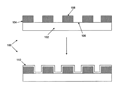
[0022] With respect to layered substrates, a schematic illustration of
the substrates of
the invention is provided in Figure 1. As shown in the upper panel, the
overall substrate 100
includes a base substrate layer 102. As noted herein, such base substrate may
include any of
a variety of different materials, including transparent materials, such as
glass, fused silica,
quartz or a polymeric material. A second, discontinuous layer 104 is provided
on the surface
of base substrate layer 102. The discontinuous layer 104 is typically
comprised of a material
that is different from the underlying substrate layer 102. By way of example,
and as noted
elsewhere herein, for certain optical applications, the discontinuous layer
104 typically
includes an opaque or non-transparent material, including, e.g., a metal
layer, a
semiconductor layer, or the like. The discontinuous layer 104 includes
openings to the
underlying surface 106 of the underlying base substrate layer 102. As a result
of the
exposure of portions of surface 106 the underlying substrate layer 102, and
the surface 108
of the discontinuous layer 104, the overall surface of the substrate 100
includes regions that
are comprised of different materials, and as a result, include different
properties. In
accordance with the invention, and as shown in the lower panel, a coating
layer 110 is
provided over the discontinuous surface to provide a substantially uniform
surface on the
overall substrate 100.
6
CA 02631248 2008-05-28
WO 2007/064597 PCT/US2006/045429
[0023] In alternative aspects, and as shown in Figure 2, the coating
layer 210 may be
provided only over the surface of one of the materials that make up the
overall surface of the
substrate 200, e.g., the discontinuous layer 104, by utilizing a coating
material that
associates preferentially with that material. This aspect may be useful where
the coating
layer results in a surface that is substantially similar to the underlying
substrate layer 102 or
its surface 106, thus yielding a substantially uniform surface over the entire
substrate 200.
In general, one could utilize the differential properties of the two different
materials to tune
the association of the coating material to the discontinuous layer. In
particular, in the case of
metal/glass hybrid surfaces, the glass surface will typically comprise a
negative charge,
while a metal oxide surface, e.g., aluminum oxide, may be positively charged.
By coating
with a negatively charged coating material, e.g. a negatively charged silane,
polymer, or the
like, one may gain selective coating of only the metal surfaces.
[0024] As will be appreciated by the skilled artisan, substrates
conforming to this
general configuration have a variety of applications. For example, layered
substrates may be
employed to provide structural components upon an otherwise planar surface,
e.g., to
provide posts, wells, channels, troughs, trenches, or the like, for
exploitation in the
localization, direction, and/or observation of materials over the surface of
the device.
[0025] Likewise, such layered structures may be used to provide layers of
differing
functionality, e.g., providing electrically conductive components over the
surface of an
otherwise insulating substrate to provide electrical access to one or more
regions of the
surface of the overall device, e.g., to drive electrophoretic movement of
materials, sense
reactions, e.g., in potentiometric or field effect sensors, etc.
[0026] Such substrates may additionally be used to provide optical
features upon an
otherwise uniform substrate material. Examples of such optical features
include simple
components, such as merely providing an isolated window for observation of a
reaction fluid
within a selected region of the surface of the overall substrate.
Alternatively or additionally,
such optical components may provide for optical manipulation of incident or
emitted light
from or through the substrate, e.g., as an optical grating or optical
confinement, i.e., a
waveguide, a zero mode waveguide, as a mask for perfouning selective optical
analyses, or
for performing diffrential optical analysis, e.g., using optical filtering
regions, or the like.
[0027] The various applications of mixed material substrates, as
described above,
envisions a broad range of different materials that range from transparent
materials to
7
CA 02631248 2013-07-10
opaque, from organic to inorganic, from conductive to semiconductive to
insulative, and to a
variety of different structures, including layered structures, discontinuously
layered
structures, embedded structures or materials, and the like. While the present
invention is
applicable to this full range of applications, materials, and structures, for
ease of discussion,
the present invention is generally illustrated in terms of the most preferred
application of a
discontinuous opaque, and preferably metal, layer disposed upon a planar
transparent
substrate layer that is preferably a rigid material. Particularly preferred
examples of such
substrates include transparent silica based substrates, such as glass, quartz,
fused silica, or
the like, having a discontinuous metal layer disposed upon its surface where
the
discontinuities in the metal layer provide apertures through the metal layer
for observation of
events upon or adjacent to the exposed surface of the underlying transparent
substrate layer.
Particularly preferred embodiments of such substrates include, for example,
waveguide
structures and zero mode waveguide structures, where a metal layer is
deposited upon a
transparent substrate as a cladding for the waveguide, and apertures are
disposed through the
metal layer to provide the core of the waveguide. Zero mode waveguides are
described in,
for example, U.S. Patent No. 6,917,726.
10028] Briefly, such zero mode waveguides typically comprise a metal
cladding
layer, e.g., aluminum, deposited upon an underlying transparent substrate
layer, e.g., glass,
quartz or fused silica. Small apertures are disposed through the cladding
layer to the
underlying substrate, and form a core region for the waveguides. As an
aperture through the
cladding layer, in application in chemical or biochemical analyses, the core
is typically filled
with the analytical reaction fluid. The cross sectional dimension of the core
is typically
sufficiently small as to prevent light of a frequency that is greater than a
cut-off frequency
from propagating completely through the zero mode waveguide. For typical
chemical and
biochemical analyses that rely upon light direction and detection for light of
wavelengths
400 urn to about 900 urn, this cross sectional dimension will typically be
from about 10 urn
to about 200 nm, and in some cases between about 20 urn and about 100 urn. As
a result
light directed at one end of the core, e.g., through the transparent substrate
layer, will only
penetrate the core a short distance.
[0029] The result is the effective illumination of a very small volume of
the core
region at the base of the waveguide. This small volume illumination is
particularly useful
8
CA 02631248 2013-07-10
for analysis of single molecule or few molecule reactions (e.g., as described
in published
U.S. Patent Nos. 7,033,764, 7,052,847, 7,056,661, 7056676.
100301 Other exemplary substrates along this line include those that
utilize an opaque
aperture to provide limited access to or from an observation region, so as to
restrict what is
being observed, either by limiting illumination or emission from such region.
[0031] A variety of other devices fit the general profile of the substrates
that are
improved by the present invention, including micro electromechanical systems
(MEMS), in
which metal or other different material layers are used to provide conductive
paths to
different regions of the substrate surface, or otherwise to provide a varied
functionality of
the surface.
[0032] The presence of a discontinuous metal layer disposed upon a
different
material provides the potential of differential interactions of the various
surface components
with the surrounding environment, and particularly in the case of fluidic,
reactive
environments. By way of example, the nature of a metal surface in a high ionic
strength
aqueous environment is substantially different from that of a silica based,
e.g., glass surface.
Initially, such surfaces will potentially have substantially different
interactions with reactants
within the aqueous system based upon differing charges and relative
hydrophobicity. In the
case of biochemical reactions, such differential reactions can impact critical
reagents, such
as substrates and products, proteins, enzymes, cofactors, labeled materials,
cells, salts, and
the like. One of the most problematic differential interactions results from
the preferential
localization (or repulsion) of one or more reactants to a particular component
of the surface.
Preferential localization of a particular reagent or product can result in
aberrant results
stemming from locally high or low concentrations of the given reagent,
excessive signal
noise resulting from optically active components localizing in one or more
locations, and the
like.
[0033] In addition to adverse impacts on reactants within an observed
reaction
system, interactions between reaction components and a portion of the surface
of the device
can also have adverse impacts upon one or both substrate layers. For example,
in the case of
metallic layers in contact with aqueous systems, and particularly high ionic
strength aqueous
solutions, such layers may be subject to degradation, corrosion or other
conversion that
adversely impacts their operation.
9
CA 02631248 2008-05-28
WO 2007/064597
PCT/US2006/045429
[0034] The present invention generally provides the above-described mixed
material
substrates with a uniform coating of an additional layer of material that
provides a
substantially uniform and preferably substantially continuous layer over the
hybrid surface
of the first and second layers. Provision of such a unifonn surface over a
hybrid surface
provides an opportunity to select a coating material that is most compatible
with the ultimate
application environment of the surface. For example, in terms of chemical or
biochemical
analyses, such surfaces are generally exposed to aqueous reaction mixtures
that may range in
salt concentrations from salt free to multimolar salt concentrations, and may
range from
highly acidic to highly basic, e.g., from pH 2.0 to 9Ø For purposes of the
invention, such
environments are referred to as chemical environments.
[0035] Alternatively or additionally, provision of a uniform, and
preferably
substantially continuous, surface layer over a hybrid material surface
provides a single
material surface against which the environmental conditions may be optimized
for minimal
adverse interactions. Such environmental conditions might include an ultimate
application,
e.g., exposure to reagents, buffers, and the like, in an analytical
application, or it may
include a subsequent treatment step, e.g., further surface modification,
whereby one has
converted a hybrid surface to a uniform surface for further manipulation.
[0036] As noted above, in some aspects, the additional coating layer may
be
selectively applied to one material region and not the other, so as to yield a
resulting surface
that has uniform properties, at least with respect to some, if not all
chemical and/or physical
properties, e.g., including the particularly relevant chemical or physical
properties of
interest. Thus, as used herein, uniformity of a surface may apply to one or
more chemical
and/or physical properties of the surface, and with respect to chemical
analyses will typically
include such properties as chemical composition of the surface, surface charge
or zeta
potential of the surface, relative hydrophobicity or hydrophilicity of the
surface, oxidative or
reductive potential of the surface, surface roughness, availability and
density of reactive
moieties on the surface, including the reactivity of such groups toward
derivatizing
chemicals, and the like. For example, where surface charge is the most
critical component, a
coating layer that provides for uniform surface charge for the overall mixed
material surface
would be termed uniform.
[0037] In
addition to providing benefits for interaction with reagents, provision of a
uniform and preferably substantially continuous coating layer over a hybrid
material surface
CA 02631248 2008-05-28
WO 2007/064597 PCT/US2006/045429
can provide protection for the underlying surface components from adverse
impacts of
reagents or reactive environments with the underlying surface components,
e.g., that might
cause corrosion or conversion of one or more of the surface components. Such
adverse
impacts are accentuated in hybrid material systems that may not be selected
for
compatibility with each of the different materials on the substrate.
[0038] A variety of different coating materials may be applied to the
hybrid surfaces
of the invention, including organic coatings such as polymers, e.g., PEGs,
fluorinated
polymers, i.e., polytetrafluoroethylene (Teflon ), organosilicates, i.e.,
methylsilsesquioxanes (MSQ), organosilanes, i.e., PDMS, and inorganic
coatings, i.e.,
silicon oxides (Si0), e.g., Si02, spin-on glass (SOG), and the like. As noted
above, a
number of different materials comprise silica based materials, e.g., glass,
quartz, silicon,
PDMS, and the like.
[0039] The method used to apply the coating layer will typically depend,
to some
extent upon the material that is to be coated. In general, however, liquid
phase or vapor
phase coating techniques are generally used in accordance with the present
invention, as are
sputtering methods for applying coating materials. Liquid phase methods
include spin
coating methods, immersion methods, self assembly (e.g., of monolayer,
bilayer, or other
film coatings) processes. Such methods may include additional curing or
conversion steps
to finish the coating layer, e.g., a thermal curing or annealing step, in the
case of spin-on
glass and silicate polymers.
[0040] Vapor deposition methods include chemical vapor deposition (CVD)
methods, including plasma enhanced methods (PECVD), molecular vapor deposition
(MVD), atomic layer deposition (ALD). Sputtering methods for provision of
uniform
layers are also useful in the context of the invention, e.g., sputtering
uniform silicon oxide
layers over a mixed material substrate. These and a variety of other coating
methods are
generally known in the art of semiconductor fabrication and processing.
[0041] As noted previously, a particularly preferred application of the
present
invention is to optical confinement structures, like zero mode waveguides, and
arrays of
such structures. Zero mode waveguides generally comprise a cladding layer that
surrounds a
core region through which electromagenetic energy is propagated. In preferred
aspects, the
core comprises an opening disposed through the cladding layer, e.g., the core
material is air
or other present fluid. The dimensions of the waveguide are typically selected
so that
11
CA 02631248 2013-07-10
electromagnetic energy that enters the core is propagated only partially
through the core.
See, e.g., Levene et al., Science (2003) 299:682-686.
100421 In preferred contexts, waveguides or waveguide arrays are defined by
a metal
cladding layer disposed over a transparent substrate, e.g., glass, quartz,
fused silica, or
transparent polymer, such that the resulting surface comprises both metal and
the transparent
substrate. In the case of fused silica, it will be readily appreciated that
the surface properties
of the metal cladding, e.g., aluminum, chromium, or the like, are very
different from the
highly charged fused silica surfaces. Typically, such metal layers are
deposited upon
underlying substrates utilizing well known IC processing techniques, such as
thermal
evaporation, sputtering, and the like. As noted above, other methods may be
employed to
generate differential material surfaces where metals are not employed,
including ion
implantation, embedding of polymer layers via lamination etc.
[00431 Where the above-described arrays are to be applied in chemical and
biochemical analyses, the differential surface properties can have an even
greater impact in
interacting differently with components of analyses, e.g., reagents such as
enzymes,
substrates or products, buffers, salts, or the like.
100441 Accordingly, when applying these waveguide structures to chemical or
biochemical analyses, it is generally desirable to provide a uniform and
preferably
substantially continuous layer over the metal layer and the exposed regions of
the underlying
substrate. As stated herein, this provides a single surface against which
subsequent surface
environments may be optimized, including, for example treatments for
immobilizing
reaction components within the waveguide cores, treatments for passivating the
surface
against excessive adsorption of reagents that might interfere with the desired
analysis, e.g.,
fluorescent molecules that might provide excessive background signal, or the
like.
Examples of waveguide structures including such surface treatments are
described, for
example, in U.S. Patent No. 7,763,423, filed September 30, 2005.
Such methods typically
employ diluted surface functionalities, e.g., diluted during or after their
adsorption or
coupling to the surface.
[0045] By way of example of the application of the invention to methods of
performing analytical reactions, U.S. Patent 7,033,764
12
CA 02631248 2013-07-10
describes elegant single molecule DNA sequencing
processes and systems that would benefit from the methods and devices
described herein.
Briefly, arrays of zero mode waveguides, e.g., configured in accordance with
the present
invention, may be employed as optical confinements for single molecule DNA
sequence
determination. In particular, as noted above, these ZMWs provide extremely
small
observation volumes at or near the transparent substrate surface, also termed
the "base" of
the ZMW. A nucleic acid synthesis complex, e.g., template sequence,
polymerase, and
primer, that is immobilized at the base of the ZMW may then be specifically
observed
during synthesis to monitor incorporation of nucleotides in a template
dependent fashion,
and thus provide the identity and sequences of nucleotides in the template
strand. This
identification is typically accomplished by providing detectable label groups,
such as
fluorescent labeling molecules, on the incorporating nucleotides. In some
instances, the
labeled nucleotides terminate primer extension, allowing a "one base at a
time" interogation
of the complex. If, upon exposure to a given labeled base, a base is
incorporated, its
representative fluorescent signal may be detected at the base of the ZMW. If
no signal is
detected, then the base was not incorporated and the complex is interrogated
with each of the
other bases, in turn. When a base is incorporated, the labeling group is then
removed, e.g.,
through a photocleavable linking group, and where the label was not the
terminating group,
a terminator, upon the 3' end of the incorporated nucleotide, may be removed
prior to
subsequent interrogation.
[0046] In alternate and preferred arrangements, the nucleotide analogs are
labeled
upon one or more of the beta, gamma or other terminal phosphate groups (in the
case of tetra
or pentaphosphate nucleotide analogs; see, e.g., U.S. Patent No. 7,041,812.
As a result, the process of
incorporation cleaves the labeling group automatically, allowing real-time
advancement of
the synthesis reaction. Further, because the incorporation event results in
prolonged
retention of the incorporated nucleotide (and its associated label) within the
observation
volume of the ZMW, that event can be readily detected. As will be appreciated,
the use of
single molecule detection methods further enhances the desirability of
providing controlled
surface interactions with the reaction environment.
[0047J In the context of the use with zero mode waveguides, as well as
other
applications, the application of a uniform coating may be carried out to
provide a coating
13
CA 02631248 2008-05-28
WO 2007/064597 PCT/US2006/045429
having a desired thickness, in accordance with known processes. In particular,
and merely
by way of example, a layer may be desired that is substantially uniform and
continuous, e.g.,
impermeable to water, while at the same time not being too thick so as to
place reaction
volumes outside of the observation region of a waveguide core. In other cases,
a selected
thickness may be desired to provide reactants at an optimal position relative
to the base of
the core, the metal cladding or other structural or optical elements of the
system. As noted,
controlling thickness of layers deposited using the methods described herein,
may be
accomplished by a variety of known methods, including time controlled vapor
deposition
processes, concentration controlled fluid based methods, and/or controlled
sputtering
processes, and the like.
[0048] In accordance with the foregoing or any aspect of the invention,
it will be
appreciated that multiple coating steps may be employed to achieve the desired
coating. In
particularly preferred aspects, e.g., in the case of PDMS coatings, multiple
coatings followed
by immersion in water or other aqueous solutions has been shown to reduce non-
specific
adsorption of dyes to surfaces. As such, the uniform coatings of the invention
may be
derived from multiple disparate steps, e.g., a coating step followed by an
oxidation step or
other coating step, in order to achieve desired surface properties.
[0049] As will be appreciated, the substrates of the invention are also
typically
included within kits for carrying out desired applications, that include
appropriate reagents
for the reaction, that may be provided in pre-measured, volumes and or
concentrations for
ease of use, along with instructions for carrying out the reactions of
interest. For example, in
the case of sequencing reactions, such kits, in addition to including the
substrates described
herein, will typically include one or more of four different nucleotides or
nucleotide analogs,
e.g., bearing fluorescent labels, nucleic acid polymerase enzymes, in some
cases primer
sequences, and additional adjunct reagents, e.g., buffers, salts, and the
like.
[0050] The substrates of the invention will also typically be used in
conjunction with
overall systems for monitoring and evaluation of the reactions carried out
upon the
substrates. An example of such a system is illustrated in Figure 5. As shown,
the system
500 will typically include a substrate of the invention 502. In the case of
fluorescence based
detection of reactions, the system will typically include a light source such
as laser 504, that
is positioned to direct light of an appropriate wavelength through an optical
train that may
include a variety of optical elements such as dichroic 506, and objective lens
508, where the
14
CA 02631248 2013-07-10
optical train is positioned to the light at the substrate 502. Additional
optical elements may
be included within the optical train, including for example, beam splitters to
provide
multiple excitation beams directed at the substrate for multiplex
applications, beam
linearizers, for simultaneous illumination of larger areas of substrates.
Fluorescent signals
emitted from the substrate or the reactions being carried out thereon, then
pass back through
optical train and optionally through additional fluorescent signal processing
components,
e.g., prism 510, focusing lens 512, until they impinge upon a detector, such
as charge
coupled device (CCD) or electron multiplying CCD (EMCCD) 514. A variety of
different
types of detectors may be employed in the context of the invention, including
photomultiplier tubes (PMTs), photodiodes, avalanche photodiodes, and the
like. In
preferred aspects, however, imaging detectors are preferred, such as diode
array detectors,
CCDs, ICCDs, EMCCDs and the like.
[0051] The signals detected by EMCCD 514 are then passed to a processor,
such as
computer 516 where they may be subjected to signal and data processing to
yield a user
interpretable manifestation of the data, e.g., in a data plot, sequence
readout, or the like.
Optical systems for use in the invention have been generally described in co-
pending PCT
Application No. US 2006/38243, and U.S. Patent No. 7,692,783.
Examples
Example 1: Vapor Deposited PDMS on Hybrid Zero Mode Waveguide Array Substrates
[0052] A zero mode waveguide array that included an aluminum cladding layer
surrounding waveguide cores of approximately 50 nm, was subjected to a plasma-
based
PDMS deposition process.
[0053] The waveguide arrays (aluminum cladding on fused silica substrate)
were
prepared with an acetone wash, isopropanol rinse and nitrogen drying. The
arrays were then
placed onto a chip holder or a glass slide and plasma treated with the
cladding layer up, for 5
minutes (Harrick, Inc., Medium power level setting, 1900-2000 mTorr). The
waveguide
arrays were then attached to the slide using a UV curable adhesive
(Norland1/481) so that the
array pane of the waveguide was opened to a hole in the slide, which created a
well around
the array suitable for fluid application.
* Trade-mark
CA 02631248 2013-07-10
10054] A polydimethylsiloxane (PDMS) gasket, precut to fit the slide, was
then
placed onto the slide. The mounted chip was then plasma treated for 1 minute
(Low power
level setting, 1900-2000 mTorr). Water was deposited in the slide well
receptacle, and the
device was allowed to incubate at room temperature for between abourt 0,5 and
2 minutes.
The water was removed and the device allowed to dry. The resulting devices
were then
assayed to determine the level of background signal resulting from non-
specific association
of fluorescent nucleotide analogs. The steps of plasma treatment, water
incubation were
then repeated up to 5 times.
[0055] Figure 3 shows a plot of fluorescent burst frequency (fluorescent
pulses)
resulting from non-specific interaction of two different fluorescent reagents
(A1exa546- and
A1exa488- labeled nucleoside tetraphosphate analogs, channel 1 and 2,
respectively) within
the observation region of zero mode waveguides. As can be seen, multiple
cycles of plasma
assisted deposition of PDMS, or its silane derivatives, yields a substantial
quieting of the
surface to background noise.
[0056] Similarly, a comparison of time-plots, as shown in Figure 4, of non-
specific
fluorescent signal intensities in a single cycle PDMS deposition (upper panel)
process versus
a multiple cycle process (lower panel, 5 cycles of Plasma/PDMS Deposition)
shows a
decided decrease in background fluorescent noise.
[0057] Although described in some detail for purposes of illustration, it
will be
readily appreciated that a number of variations known or appreciated by those
of skill in the
art may be practiced within the scope of present invention. Unless otherwise
clear from the
context or expressly stated, any concentration values provided herein are
generally given in
terms of admixture values or percentages without regard to any conversion that
occurs upon
or following addition of the particular component of the mixture.
16