Note: Descriptions are shown in the official language in which they were submitted.
CA 02642337 2014-05-01
- I -
HIGH POWER, POLARIZATION-DIVERSE CLOVERLEAF PHASED ARRAY
FIELD OF THE INVENTION
The present invention relates, in general, to an antenna and, more
specifically, to a
phased array antenna including multiple radiating elements arranged in a
cloverleaf pattern. The
phased array operates over multi-octave bandwidths, subtends a wide field-of-
view, and
responds to any desired polarization in space. The phased array is amenable to
conformal
installation and may transmit at high peak and high average power.
BACKGROUND OF THE INVENTION
Significant advances in broadband solid-state power generation have placed a
new
emphasis on phased arrays to efficiently combine the power of individual
devices into high-
power transmissions by exploiting the magnification property of phased arrays,
known as the
"array factor". Commensurate with this trend, the demands for high transmitted
effective
radiated power (ERP) have increased by as much as an order of magnitude. In
addition,
operating frequency range has been lowered into the HFNHF region.
Along with the high effective radiated power, the multi-functional performance
characteristics associated with phased arrays, such as multi-octave
bandwidths, wide field-of-
view, instantaneous multiple beams and polarization agility, must also be
maintained.
Within the context of these requirements, emphasis must now be given to issues
related
to power handling within the array aperture, as well as the entire corporate
feed structure.
Power handling encompasses not only the capacity to sustain peak and average
(CW) power
demands, but also to be able to operate in adverse temperatures on the phased
array.
The present application is related to U.S. Patent No. 6,992,632 issued to
Mohuchy on
January 31, 2006, entitled "Low Profile Polarization-Diverse Herringbone
Phased Array", and
U.S. Patent 6,853,351 entitled "Compact High-Power Reflective- Cavity Backed
Spiral
Antenna", issued to Mohuchy on February 8, 2005.
22546341.1
CA 02642337 2014-05-01
- 2 -
According to one aspect of the present invention, there is provided a phased
array
antenna comprising a substrate, and multiple radiating elements conformally
mounted as micro-
strips on the substrate, wherein each of the radiating elements is of a
triangular shape, four of
the radiating elements are arranged to form a crossed bowtie cloverleaf
radiator, each of the
triangular shaped radiating elements includes a vertex formed by two equal
sides of an
isosceles triangle extending from a base, and a line extending from the vertex
and intersecting a
midpoint of the base of the isosceles triangle forms a 45 degree angle with
respect to a scan
axis of the phased array antenna.
According also to a further aspect of the present invention, there is provided
a phased
array antenna comprising a substrate, and multiple crossed bowtie cloverleaf
radiators
conformally mounted as micro-strips on the substrate, wherein each crossed
bowtie cloverleaf
radiator is shaped as identical first and second bowtie configurations, the
first and second
bowtie configurations are oriented orthogonally to each other, each radiating
element has a
shape of an isosceles triangle, with a launch point disposed adjacent to a
vertex opposite to a
base of the isosceles triangle, a scan axis for the phased array antenna, and
a line extending
from the vertex and intersecting a midpoint of a base of the isosceles
triangle forms a 45 degree
angle with respect to the scan axis.
According to a still further aspect of the present invention, there is
provided a phased
array antenna comprising multiple crossed bowtie cloverleaf radiators mounted
on a first
dielectric layer, cooling channels disposed within a second dielectric layer,
and a metallic
ground formed as a third layer, wherein the first, second and third layers are
disposed in a
sequence of first, second and third layers, each of the crossed bowtie
cloverleaf radiators
includes at least two sets of four radiating elements arranged in a cross-
configuration, and the
at least two sets of four radiating elements are mounted on a single,
continuous layer of the first
dielectric layer.
Embodiments of the invention will now be described by way of example only.
22546341.1
CA 02642337 2014-05-01
- 3 -
BRIEF DESCRIPTION OF THE DRAWINQ
The invention is best understood from the following detailed description
when read In conjunction with the accompanying drawing. Included in the
drawing are
the following figures:
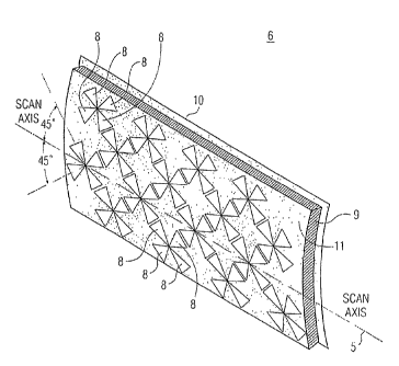
FIG. 1 is a partial perspective view of multiple radiating elements, each
configured in a triangular pattern, where two orthogonal pairs of radiating
elements
form a crossed bowtie cloverleaf radiator that is oonformaily mounted as micro-
strips
on a multilayer substrate to form a planar phased array antenna, according to
an
embodiment of the present invention;
FIG. 2A is a perspective view of a single crossed bowtie cloverleaf
radiator of the planar phased array shown in FIG. 1, including four RF center
conductors
each connected to a respective radiating element of the single crossed bowtie
cloverleaf
radiator, according to an embodiment of the present invention;
9G. 2B is a top cross-sectional view of a dielectric spacer for receiving
four RF center conductors for connection to four respective launch points of
the single
crossed bowtie cloverleaf radiator shown in FIGS. 2A and 2C, according to an
embodiment of the present invention;
FIG. 2C is a front cross-sectional view of the single crossed bowtie
cloverleaf radiator and its corresponding RF center conductors shown in FIG.
2A (only
two RF center conductors are shown), according to an embodiment of the present
invention;
FIG. 3 is a close-up view of a single crossed bowtie cloverleaf radiator
composed of four triangular radiating elements of the planar phased array
shown in
FIG. 1, according to an embodiment of the present invention;
FIG. 4 is an interior cross-sectional view of the RF feed from four RF
center conductors to the four launch points of the crossed bowtie cloverleaf
radiator of
the planar phased array shown in FIG. 1, according to an embodiment of the
present
invention; =
FIG. 5 is a detailed view of a single RF center conductor, employed in the
o RF feed to the crossed bowtie cloverleaf radiator of the planar phased
array shown in
FIG. 1, according to an embodiment of the present invention;
FIG. 6 is a cross-sectional view of the channeled, or fluted core layer,
which is shown sandwiched in FIG. 1 between a metallic ground layer and a
substrate
CA 02642337 2014-05-01
¨4 ¨
layer that includes a chemically etched planar phased array, according to an
embodiment of the present invention;
FIG. 7 is a plot of input return loss versus frequency of a prototype
crossed bowtie cloverleaf planar phased array shown in FIG. 1, according to an
embodiment of the present invention; and
FIGS. 8A, 88, 8C and SD are sample radiating patterns of a prototype
crossed bowtie cloverleaf planar phased array shown in FIG. 1, according to an
embodiment of the present invention.
DETAILED DESCRIPTION OF THE INVENTION
io Referring to FIG. 1, there is shown a partial perspective view
of a phased
array antenna, generally designated as 6, in accordance with an embodiment of
the
present invention. As shown, phased array antenna 6 includes multiple
radiating
elements 8, where each radiating element 8 is of a triangular shape. Four (4)
radiating
elements 8 are arranged as two (2) orthogonal pairs in a cloverleaf pattern,
also
referred to herein as a crossed bowtie cloverleaf radiator. The orthogonal
pairs of
elements 8 are formed conformally on thin substrate 11 and are disposed in a
triangular grid according to the following relationship, which excludes the
appearance
of grating lobes:
Ais = 1 -I- sin 0
where: A is the wavelength at the highest operating frequency,
s is the element spacing in the scanning direction,
is the maximum array scan angle.
The orthogonal pairs of radiating elements 8 are positioned at 45 degrees
relative to a scan axis of the phased array antenna, generally designated as
5.
Although the scan axis is shown oriented along the X-axis, it will be
appreciated that
the scan axis may be oriented along the Y-axis, or any other angular
orientation. The
scan axis, for example, may also be of a conical scan orientation.
The substrate 11 is mounted on a fluted core layer of dielectric material,
designated as core 9. The layer of core 9 is supported by a reflective,
metallic ground
so plane, designated as 10. For discussion purposes, FIG. 1 shows only
sixteen crossed
= bowtie cloverleaf radiators. The phased array antenna may Include more or
less than
sixteen crossed bowtle cloverleaf radiators and may be arranged in a different
triangular grid or aspect ratio.
CA 02642337 2014-05-01
¨ 5 ¨
The cloverleaf structure is shown in more detail in FIGS. 2A, 28 and 2C.
The RF signal is inputted or received by means of a coaxial transmission
medium, two
of which are shown as coaxial portions 25 and 26 In FIG. 2A (only two coaxial
portions
25 and 26 are visible in FIG. 2C; the other two orthogonal inputs are not
included In
the figure). Coaxial portions 25 and 26 include, respectively, coaxial
conductors 21A
and 22A, as shown.
Coaxial conductors 21A and 22A each forms one end of RF center
conductors 21 and 22; wide center conductors 218 and 2213 each forms a central
portion of RF center conductors 21 and 22; and thinned center conductors 21C
and 22C
to each forms the other end of RF center conductors 21 and 22. It will be
understood that
the coaxial conductor of the coaxial portion, the wide center conductor and
the thinned
center conductor form one continuous RF conduction path for coupling the RF
signal
from the input side to the output side of the radiating elements.
The RF signal is received via the four RF center conductors 21, 22, 23
ts and 24 (only RF center conductors 21 and 22 are visible in FIG. 2C; and
four RF center
conductors 21, 22, 23 and 24 are visible in FIG. 2A). The four RF center
conductors
terminate at four respective launch points of the crossed bowtie cloverleaf
radiator,
which includes four respective radiating elements 8. Accordingly, each of the
four RF
center conductors terminates at a corresponding launch point of one of the
four
zo radiating elements 8.
The four RF center conductors 21, 22, 23 and 24 extend sequentially
through metallic ground plane 10, fluted core 9 and substrate 11, as shown in
FIG. 2C
(for clarity, only RF center conductors 21 and 22 are shown in FIG. 2C). The
four RF
center conductors 21, 22, 23 and 24 are supported at the feed end by four
respective
25 bulkhead coaxial connectors, one shown as 60 in FIG. 5. The same four RF
center
conductors are supported at the crossed bowtie cloverleaf end by a tailored
dielectric
spacer, shown as 40 in FIGS. 28 and 2C.
As best shown in FIGS. 2C and 5, each RF center conductor includes a
coaxial conductor, originating at metallic layer 10 and extending through
dielectric
39 sleeve 25, 26. Each coaxial conductor is connected (described below),
after leaving the
dielectric sleeve, to wide conductor 21B, 228, 235 and 245. Each wide
conductor
extends into a thinned conductor, each designated as 21C, 22C, 23C and 24C.
The
thinned conductors, in turn, pass through holes 41 of dielectric spacer 40
(FIG. 2B).
The multiple radiating elements 8 are chemically etched on copper clad
35 dielectric material, which forms substrate layer 11, in the manner
depicted in FIG. 3.
CA 02642337 2014-05-01
¨ 6 ¨
Connectivity to RF center conductors 21, 22, 23 and 24 is achieved with flat
socket
screws 51 to assure good contact between a respective RF center conductor and
a
launching point of a radiating element. One flat socket screw 51 is also shown
in FIG. 5
with washer 51A interposed between socket screw 51 and thinned center
conductor
S 21C, 22C, 23C and 24C.
FIG. 4 illustrates the relative position of the thinned center conductors,
designated as 21C, 22C, 23C and 24C, within fluted core 9 and the attachment
points
of respective flat socket screws 51 into threaded cores 51B, the latter formed
into each
thinned center conductor. By passing flat socket screws 51 through substrate
11 at
io respective excitation ports of the bowtie radiators (FIG. 3) and
threading them into
threaded cores 51B, a solid connection is effectively made between the RF
center
conductor and its corresponding radiating element 8.
It will be appreciated that a portion of fluted core 9 is removed in the
area of the four RF center conductors 21, 22, 23 and 24 to preclude contact
with the
is core material and permit convective cooling. The core material is
removed in area 40
of FIG. 4 which corresponds to the area of dielectric spacer 40 of FIG. 2B. In
this
manner, the tailored dielectric spacer 40 may nest in the removed portion of
fluted core
9.
The RF center conductor, as shown in FIG.5, includes a coaxial bulkhead
w connector 60 with its dielectric sleeve 25, 26 extending a distance T
that corresponds to
the thickness of metallic ground plane 10. The coaxial conductor of coaxial
bulkhead
connector 60 is positively joined to wide RF conductor 21B, 22B, 23B, 24B with
set
screw 61.
The four RF center conductors for a given crossed bowtie cloverleaf
!s radiator are arranged as a balanced twin-lead transmission line pair.
Each RF center
conductor has a varying cross-sectional diameter along its length, so that it
is thinner
at its output end adjacent each radiating element 8. This=thinning of the RF
center
conductor advantageously allows matching the excitation ports of the bowtie
radiators
with respect to a driving point impedance desired to achieve minimum signal
reflection.
The socket set screw 51 caps thinned center conductor 21C, 22C, 23C, 24C for a
positive connection to a bowtle radiator input.
The fluted core 9 in FIG. 6 is a layered composite of dielectric material
(one or more materials) that is channeled for coolant passage in either a
vertical or
horizontal orientation with respect to the scan axis of the phased array
antenna,
i5 depending on the physical disposition of the coolant. The layers,
denoted as having a
CA 02642337 2014-05-01
¨7 ¨
thickness H, may be of one-inch thickness. One-half of the thickness H Is a
solid,
shown designated as 71, and the other one-half of the core thickness H is
fluted, shown
designated as 72. The width of solid core 71 and the width of removed, or
fluted core
72 are equal. The overall, total height of the fluted core (shown as 4H) is
s approximately equivalent to a quarter wavelength at the high frequency of
the desired
band.
A proof-of-concept phased array antenna, as embodied in the above
described figures, was fabricated and measured in the 670-2000 MHz frequency
band.
The baseline for the phased array radiating aperture was determined using the
general
w guidelines for biconical antennas, as outlined in Kraus, "Antennas",
Second Edition,
published by McGraw-Hill Book Co, 1988, chapter 8. Chapter 8 is incorporated
herein
by reference in its entirety. The initial dimensions were then optimized using
a three-
dimensional method-of-moments (MOM) tool that allowed construction of an array
of
crossed bowtie cloverleaf radiators. The resulting radiation patterns and
driving port
is impedances, taking into consideration mutual impedance contributions,
were
computed.
The element dimensions were specifically optimized for a maximum
operating bandwidth over a 120 degree field-of-view. The main tradeoff
parameters, as
shown in FIG. 3 were the length, L, of the bowtie (or a pair of radiating
elements 8);
w the width, W, of the bowtie (or the pair of radiating elements 8); and
their inter-
element spacing, shown as gap, G, between one bowtie and another adjacent
bowtie.
From a network point of view, the length L behaves as an inductive
component, while the width W and the adjacent element gap G represent
capacitance.
The combined effect is a tank circuit which may be optimized for maximum
operating
ts bandwidth.
It will be appreciated that this optimization must Include the entire field-
of-view, because mutual coupling between adjacent elements varies
significantly with
the scan angle. A practical solution may be to focus on all scanned angles up
to +1- 45
degrees. Beyond the 45 degree scan coverage may be provided by pattern beam
io broadening effects.
A good indicator of array performance is the array VSWR (Voltage
Standing Wave Ratio) for both the input to the array from the RF feed and the
return
loss seen by an incoming plane wave into the array. The desired figure of
merit for
both conditions is to operate a broadband array with a VSWR under 2:1.
Practice,
CA 02642337 2014-05-01
¨ 8 ¨
however, allows operating the array up to a 3:1 ratio, without significantly
degrading
the overall array operating efficiency.
FIG. 7 shows the optimized VSWR performance of the proof-of-concept
array. The TNC port designations refer to the array input, which was a coaxial
TNC
s type connector having a characteristic impedance of 50 ohms. The driving
point
designations refer to the aperture mismatch to an incident plane wave and are
referenced to the free space impedance of 377 ohms. The relationship between
VSWR
and Return Loss in FIG. 7 is as follows:
P = (a - 1)/(
io where: p is Return Loss in voltage ratio
cr is VSWR in voltage ratio.
The aperture dimensions derived from the optimization are:
L = 3.038 inches
W = 0.981 inches
15 G = 0.090 inches
The center to center element spacing in both the Azimuth and Elevation
directions is 2.307 inches.
The center RF conductors, shown in FIG. 5, behave electrically as
described in US Patent 6,853,351 with respect to FIG. 4 therein. The
impedance, and
zo hence the dimensions of the center RF.conductors are determined by
appreciating that
they are pairs of transmission lines connecting the input of the array to each
pair of
radiating elements 8. The center RF conductors are also approximately h/4
long, which
is an ideal electrical length for a quarter-wave transformer.
The calculated impedance at the feed points of the bowtie (or pair of
zs radiating elements 8) is 160 ohms. The RF coaxial connectors 60, when
used as a pair,
effectively represent 100 ohms. The resultant impedance then becomes 126 ohms,
which corresponds to a wide center conductor (21B, for example) having a
diameter of
0.34 inches. The center RF conductor (21, for example) is stepped down to 0.22
inch
diameter forming the thinned center conductor (21C, for example) for
approximately
lo one fourth of the total length of center conductor 21. This dimension
corresponds to
the diameter of set screw 51 used to couple the bowtie input to the respective
center
RF conductor as a means of eliminating any possibility of RF corona between
the set
screw and the center RF conductor.
CA 02642337 2014-05-01
- 9 ¨
The fluted core shown in FIG. 6, in one exemplary embodiment, includes
one dielectric material. For the proof-of-concept array structural foam was
employed
with a relative dielectric constant of 1.45. The material was available in one
inch thick
H panels, with the panels layered and thermally bonded into a single slab.
Prior to
bonding, each layer was machined to provide grooves over one half of the
height H and
spaced equally in width, with the groove position offset between adjacent
layers, as
shown in FIG. 6. The effective dielectric constant was computed on the basis
of a
volumetric average between the air and the remaining dielectric, resulting in
a relative
dielectric constant of 1.36.
Sample array patterns shown in FIG. 8 were measured with a True Time
Delay (ITD) beam steering network, described in co-pending U.S.. Patent
Application
No. 6,992,632, which also provides the means for T/12 capability and full
polarization
control. Advantages of the present invention is the implementation of a 180-
degree
phase bit to provide the required balanced field excitation at the bowtie
terminals, and
I s the elimination of the power-limited balun that has been the mainstay
of the prior art.
The sample radiation patterns in FIG. 8 are the array response to
vertically (V) and horizontally (H) polarized signals. The plots are
referenced to the net
array gain and are within the directivity predictions for the proof-of-concept
aperture,
indicating good efficiency both at boresite and when scanned to 40 degrees.
The
20 scanned beam maintains the 40-degree position over the measured
frequency band,
which is the expected performance from a TTD scanned array. At this scan
angle, the
beams broaden sufficiently to provide positive gain coverage out to 60
degrees, or a full
120-degree field-of-view.
Having described an embodiment of this invention, it is evident that
25 other embodiments incorporating these concepts may be used. For example,
frequency
scaling of the dimensions may be used to operate in other frequency bands. The
types
of fasteners, connectors or dielectrics may be varied, with the appropriate
electrical
compensation. The array may be a planar or a conformally shaped structure
deployed
to any aspect ratio commensurate with the spatial coverage required.
30 Accordingly, although the invention has been described with a
certain
degree of particularity, it is understood that the present description is made
only by
way of example and that numerous changes in the details of construction,
combination
and arrangement of parts may be made,