Note: Descriptions are shown in the official language in which they were submitted.
CA 02644946 2012-04-25
74769-2156
MODIFIED INVERTED-F ANTENNA FOR WIRELESS COMMUNICATION
[1] BACKGROUND
Field of the Invention
[2] Embodiments of the invention relate generally to radio antennas for
wireless communication systems. More particularly, the embodiments of the
invention relate to low cost compact printed circuit board (PCB) antennas for
subscriber units of wireless broadband communication systems and cellular
wireless
communication systems.
Description of Related Art.
[003] It is widely known that antennas can be used to transmit and receive
electromagnetic radiation of certain frequencies to carry signals. That is, an
antenna
is typically designed to transmit and receive signals over a range of carrier
frequencies. The antenna is a critical part of all wireless communications
devices.
Typically, antennas should meet very stringent requirements regarding size,
efficiency, wide bandwidth of operation, ability to function efficiently when
space is at
premium and a low manufacturing cost. Small space, usually available for an
antenna, dictates antenna choice, which may be a printed monopole antenna, an
L-
shaped antenna, a planar inverted-F antenna, a printed disc antenna or a patch
antenna.
[004] Small size of printed antennas, usually a quarter of operation
wavelength, is the result of a ground plate effect utilized in the antenna
design.
Induced currents form a mirror image of a radiating element on the ground
plate.
Eventually the effective size of the antenna should include a part of the
ground plate
which includes significant part of induced currents. On the other hand,
induced
currents are very susceptible to any conducting elements placed in the
neighborhood
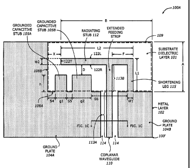
of the antenna. The commonly used approach to improve the performance of the
1
, 74769-2156 CA 02644946 2012-04-25
printed antenna is to keep the antenna away from any conducting components of
the
device. The minimum distance between antenna and RF
la
WO 2007/126897 CA 02644946 2008-09-02PCT/US2007/007694
components, considered safe in the 3 GHz frequency band is equal to about of
lcm.
Violation of this rule results in a significant impedance mismatch between an
antenna and a
transmission line, efficiency loss and a resonant frequency shift.
[5] Another factor, which significantly effects antenna performance, is the
communications device plastic casing_ Plastic casing significantly effects
radiation
efficiency of the antenna. Nevertheless, in an attempt to miniaturize a
device, designers,
practically, do not leave much space between a PCB and a plastic cover.
[6] All factors, described above, make antenna design procedure extremely
complicated
and difficult. In each particular case, not only a PCB size and position of
radio frequency
(RF) components should be taken into account, but also devices plastic body
shape and
material dielectric constant. Other design criteria of an antenna may need to
be considered,
such as costs, portability, and possibly aesthetics. These design criteria are
particularly
relevant to portable wireless communication devices that are to be marketed to
the general
public. Moreover, the size or form factor of portable wireless communication
devices poses
particular challenges in antenna design. Additionally, consumers are demanding
greater
portability, higher data bandwidth, and better signal quality in wireless
communication
devices and systems.
2
WO 2007/126897 CA 02644946 2008-09-02PCT/US2007/007694
BRIEF DESCRIPTION OF THE DRAWINGS
[7] Embodiments of invention may best be understood by referring to the
following
description and accompanying drawings that are used to illustrate embodiments
of the
invention. In the drawings:
[8] Figure IA is a top view of a first embodiment of a modified inverted-F
antenna at a
corner of a printed circuit board.
[9] Figure 1B is a top view of a second embodiment of a modified inverted-F
antenna at
a corner of a printed circuit board.
[0010] Figure IC is a cross-sectional view of the grounded coplanar waveguide
illustrated
in Figures 1A-1B.
- [0011] Figure 2A is a top view of a third embodiment of a modified inverted-
F antenna at a
corner of a printed circuit board.
[0012] Figure 2B is a cross-sectional view of the third embodiment of the
modified
inverted-F antenna along the radiating stub.
[0013] Figure 2C is a top view of a fourth embodiment of a modified inverted-F
antenna at
a comer of a printed circuit board.
[0014] Figure 2D is a top view of a fifth embodiment of a modified inverted-F
antenna at a
corner of a printed circuit board.
[0015] Figure 3A is a top view of a sixth embodiment of a modified inverted-F
antenna
along an edge of a printed circuit board.
[0016] Figure 3B is a cross-sectional view of the sixth embodiment of the
modified
inverted-F antenna along the radiating stub.
[0017] Figure 3C is a top view of a seventh embodiment of a modified inverted-
F antenna
along an edge of a printed circuit board.
[0018] Figure 4 is a top view of an eighth embodiment of a modified inverted-F
antenna
along an edge of a printed circuit board.
[0019] Figure 5 is a top view of a pair of modified inverted-F antennas in the
corners of the
PCB with grounded coplanar waveguide feeding lines for use in a CardBus
application.
[0020] Figure 6 is a linear antenna array of four modified inverted-F antennas
extruded
from the ground plates with grounded coplanar waveguide feeding lines.
3
WO 2007/126897 CA 02644946 2008-09-02PCT/US2007/007694
[0021] Figure 7 is a high level block diagram including the antenna design of
Figure 5 and a
system using switching diversity technology.
[0022] Figure 8 is a high level block diagram including the antenna design of
Figure 5 and a
system using 2x2 MIMO technology.
[0023] Figure 9 illustrates a graph of the return loss of a modified inverted-
F antenna for a
CardBus printed circuit board such as illustrated in Figure 5.
[0024] Figure 10 illustrates a chart of the far field radiation pattern in a
horizontal plane for
the CardBus modified inverted-F antenna shown in Figure 5.
[0025] Figure 11 illustrates a chart of the far field radiation pattern in a
vertical plane for
the CardBus modified inverted-F antenna shown in Figure 5.
[0026] Figure 12 illustrates a wireless communication network with subscriber
units
employing embodiments of the invention.
[0027] Figure 13A illustrates a wireless universal serial bus (USB) adapter
including a
printed circuit board with embodiments of the modified inverted-F antenna for
use by a
subscriber unit.
[0028] Figure 13B illustrates another wireless card or adapter including a
printed circuit
board with embodiments of the modified inverted-F antenna.
[0029] Figure 14 illustrates a functional block diagram of a wireless card
including a
printed circuit board with embodiments of the modified inverted-F antenna.
[0030] Figure 15 is a flowchart illustrating a process to form a modified
inverted-F antenna
according to one embodiment of the invention.
[0031] Like reference numbers and designations in the drawings indicate like
elements
providing similar functionality. Additionally, it is understood that all the
drawings of figures
provided herein are for illustrative purposes only and do not necessarily
reflect the actual
shape, size, or dimensions of the elements.
4
CA 02644946 2012-04-25
74769-2156
DESCRIPTION
[0031a] According to one aspect of the present invention,
there is provided an
apparatus comprising: a dielectric substrate having a first surface; a
radiating stub on
the first surface of the dielectric substrate; and a first ground plate on the
first surface
of the dielectric substrate to couple to ground, the first ground plate
including one or
more grounded capacitive stubs spaced apart from the radiating stub, the one
or
more grounded capacitive stubs to tune performance parameters.
[0031b] According to another aspect of the present invention,
there is provided
a method comprising: forming a dielectric layer on a first metal layer having
a first
surface; forming a pattern of a second metal layer on the dielectric layer to
expose a
dielectric window being part of the dielectric layer, the pattern having a
radiating stub
and one or more grounded capacitive stubs spaced apart from the radiating
stub; and
forming a first ground plate coupled to the one or more grounded capacitive
stubs,
the first ground plate being part of the second metal layer and coupled to
ground.
[0031c] According to still another aspect of the present
invention, there is
provided a system comprising: a base-band processor to process base-band
signals,
the base-band processor generating a transmitting signal and processing a
receiving
signal; a transceiver coupled to the base-band processor to process the
transmitting
signal and the receiving signal; a switch coupled to the transceiver to switch
between
the transmitting signal and the receiving signal; and an antenna circuit
coupled to the
switch to transmit the transmitting signal and to receive the receiving
signal, the
antenna circuit comprising: a dielectric substrate having a first surface, a
radiating
stub on the first surface of the dielectric substrate, and a first ground
plate on the
surface of the dielectric substrate to couple to ground, the first ground
plate including
one or more grounded capacitive stubs spaced apart from the radiating stub,
the one
or more grounded capacitive stubs to tune performance parameters.
[0032] An embodiment of the present invention is a modified
inverted-F
antenna for wireless communication. The modified inverted-F antenna includes
a5
CA 02644946 2012-04-25
74769-.2156
substrate, a radiating stub, one or more grounded capacitive stubs, a
shortening leg,
a ground plate on an outer layer of the substrate, an extended feeding strip,
and a
feeding transmission line. The feeding transmission line may be implemented as
a
microstrip line, a strip line, a coplanar waveguide (CPW), or a grounded
coplanar
waveguide (GCPW), and placed together with the extended feeding strip on the
same
outer layer or on different internal or other outer layer of a multilayer-
substrate and
connected to the radiating stub directly through the extended feeding strip
for the
same layer location or through the extended feeding strip and via hole for
other layer
locations. An internal and other outer substrate layers have no metal strips
in any
area of the modified inverted-F antenna excluding a layer with the extended
feeding
strip. The one or more grounded capacitive stubs tune performance parameters
of
the antenna.
[0033] In the following description, numerous specific details are set forth.
However, it is understood that embodiments of the invention may be practiced
without these specific details. In other instances, well-known circuits,
structures, and
techniques have not been shown to avoid obscuring the understanding of this
description.
[0034] One embodiment of the invention may be described as a process which
is usually depicted as a flowchart, a flow diagram, a structure diagram, or a
block
diagram. Although a flowchart may describe the operations as a sequential
process,
many of the operations can be performed in parallel or concurrently. In
addition, the
order of the operations may be re-arranged. A process is terminated when its
operations are completed. A process may correspond to a method, a program, a
procedure, a method of manufacturing or fabrication, etc.
[0035] Embodiments of the invention include a modified inverted-F antenna to
radiate and/or receive wireless communication electro-magnetic signals in a
wireless
communication system. In contrast to a base station (BS), the modified
inverted-F
antenna is designed for wireless communication subscriber stations (SS) that
may be
5a
CA 02644946 2012-04-25
74769-2156
either fixed stations (FS) or mobile stations (MS). In a typical subscriber
station, the
dimensions and performance are at premium, due to the tightly packaged RF
circuitry
and the requirement
5b
WO 2007/126897 CA 02644946 2008-09-02PCT/US2007/007694
for one or more antennas for switching diversity, Multiple Input Multiple
Output (Mliv10)
or adaptive antenna array technology applications. Example applications with a
small form
factor include wireless adapters such as a CardBus, Personal Computer Memory
Card
International Association (PCMCIA), and USB-terminal adapters as well as
laptop
computers (e.g., printed inverted F antenna (PIFA) for MiniPCI SS), Cellular
Phones, and
personal digital assistants (PDA).
[0036] The modified inverted-F printed circuit board antenna has good matching
and is
designed for such applications where active RF circuitry and other structures
are in close
proximity. In a number of embodiments of the invention, the modified inverted-
F antenna
is formed in one or more corners of the printed circuit board. In a number of
other
embodiments of the invention, the modified inverted-F antenna is formed along
an edge of
the printed circuit board.
[0037] Each embodiment of the modified inverted-F antenna includes a feeding
transmission line and an extended feeding strip that may be implemented in
different ways.
The feeding transmission line can be implemented as a microstrip line, a strip
line, a
coplanar waveguide (CPW) or a grounded coplanar waveguide (GCPW). The extended
feeding strip is formed on the same layer as the feeding transmission line and
coupled
thereto. The type of the feeding transmission line selected has little-to-no
influence on the
performance of the modified inverted-F antenna. Instead, the type of the
feeding
transmission line chosen is based on how the overall RF PCB is designed, such
as what
layers of the PCB the signals from the amplifiers are available. In some
embodiments of the
invention, the feeding line, extended feeding strip, and radiating stub are on
the same layer
of a printed circuit board and can thereby be readily connected together. In
other
embodiments of the invention, the feeding line and extended feeding strip are
on different
layers from that of the radiating stub. In this case, the feeding line and
extended feeding
strip on one layer may couple to the radiating stub by way of a via (VIA), a
hole with
metallized walls.
[0038] Referring now to Fig. 1A, a top view of a first embodiment of a
modified inverted-F
antenna 100A is illustrated. The modified inverted-F antenna 100A is an
integral part of a
printed circuit board 100 including a substrate dielectric layer 101 and an
outer conductive
metal layer 102. The pattern in the outer conductive metal layer 102 over the
substrate
dielectric layer 101 generally forms the modified inverted-F antenna 100A in
an area of a
6
WO 2007/126897 CA 02644946 2008-09-02
PCT/US2007/007694
dielectric window 109 with dimensions A x B as illustrated. In one embodiment
of the
invention, the dimension of A is 9.4 millimeters and the dimension of B is
20.8 millimeters.
The modified inverted-F antenna 100A is designed with multiple grounded
capacitive stubs
and a grounded coplanar waveguide feeding line on the same outer conductive
metal layer
102 formed on the substrate dielectric layer 101. The dielectric window in the
surface of
the dielectric substrate is partially covered over by the pattern and the one
or more grounded
capacitive stubs. That is, the pattern and the one or more grounded capacitive
stubs extend
or encroach into the dielectric window 109.
[0039] The modified inverted-F antenna 100A includes the substrate dielectric
layer 101, a
radiating stub 112, one or more grounded capacitive stubs 105A-105B, a
shortening leg
115, and one or more ground plates 104A-104B formed in the metal layer 102 on
an outer
layer of the substrate 101, as shown in Figure 1A. The one or more ground
plates 104A-
104B are to couple to ground.
[0040] The radiating stub 112 has a first side edge 122R, a second side edge
122L, and a
top edge 122T. The ground plate 104A is formed spaced apart along the first
side edge
122R and the top edge 122T of the radiating stub 112.
[0041] The one or more grounded capacitive stubs 105A-105B extend from a first
edge
108A of the ground plate 104A that is parallel with the first side edge 122R
of the radiating
stub. The height h of the one or more grounded capacitive stubs 105A-105B
points toward
the radiating stub. A second edge 108B of the ground plate 104A is
substantially
perpendicular to the first edge 108A. The second edge 108B of the ground plate
104A is
- substantially parallel with the top edge 122T of the radiating stub and
spaced apart from it
by the dimension X as illustrated in Figure IA.
[0042] The modified inverted-F antenna 100A further includes an extended
feeding strip
113B as illustrated in Figure 1A. In this case, the grounded coplanar
waveguide (GCPW)
110 is the feeding transmission line.
[0043] The grounded coplanar waveguide (GCPW) 110 includes a central strip
113A
bounded on left and right sides by the ground plates 104A-104B, each being
separated by a
gap 114. To complete the GCPW 110, the printed circuit board 100 has a ground
plate 125
(shown in Figure IC) on a second metal layer 103 (shown in Figure 1C) and
under the
central strip 113A and the gaps 114. The ground plate 125 is isolated from the
central strip
7
WO 2007/126897 CA 02644946 2008-09-02PCT/US2007/007694
113A by the dielectric layer of the substrate 101. The central strip 113A is
coupled to the
extended feeding strip 113B. The width of the central strip 113A and the gaps
114 are a
function of the wavelength of the carrier frequencies of the wireless
communication
channels and the performance of the dielectric layers of the substrate 101.
[0044] The extended feeding strip 113B couples to the radiating stub 112 at
one end and the
central strip 113A at an opposite end. The shortening leg 115 is coupled to
the ground plate
104B at one end and the radiating stub 112 at an opposite end. The length of
the shortening
leg 115 is chosen to provide a fifty (50) Ohm active input impedance for the
antenna at the
junction of the GCPW 110 to the extended feeding strip 113B. As the antenna
presents
itself as an inductive grounded stub, the input impedance of the antenna has
some inductive
reactance from the metal forming the radiating stub 112 and the shortening leg
115. Prior art
attempts to reduce this inductive reactance, such as by narrowing a gap
between the end of
radiating stub and the ground plate and by bending the radiating stub toward
the ground
plate, have been largely unsuccessful due to their limited effect on antenna
input impedance.
[0045] Referring now to Figure 1B, a top view of a second embodiment of a
modified
inverted-F antenna 100B is illustrated_ The modified inverted-F antenna 100B
has a feeding
transmission line formed on the same outer layer of the substrate on which the
antenna is
formed.
[0046] The modified inverted-F antenna 100B is similar to the modified
inverted-F antenna
100A but has only one grounded capacitive stub 105 having a width g and a
space or gap S
with ground plate 104A. In this exemplary embodiment, the edge 122R of the
radiating
stub 112 is parallel with the grounded capacitive stub 105 such that a top
edge 122T of the
radiating stub extends beyond the width g of the grounded capacitive stub 105
into the space
S.
[0047] Otherwise, the modified inverted-F antenna 100B has similar elements to
the
modified inverted-F antenna 100A and uses similar reference numbers and
nomenclature.
Accordingly, the description of the elements of the modified inverted-F
antenna 100B is not
repeated for reasons of brevity, it being understood that the description of
the elements of
antenna 100A is equally applicable to the elements of antenna 100B.
[0048] Various dimensions for elements of the modified inverted-F antenna are
shown in
the drawings. The shortening leg 115 has a width WI and length LI as shown.
The
8
WO 2007/126897 CA 02644946 2008-09-02PCT/US2007/007694
radiating stub 112 has a length L2 and a width W2 as shown. At a distance F up
the
radiating stub 112 from the shortening leg 115, the extended feeding strip
113B is coupled
to the radiating stub 112 as shown. The positioning of the antenna in the
dielectric window
109 along the A dimension is established by the length LI of the shortening
leg 115. The
positioning of the antenna in the dielectric window 109 along the B dimension
is established
by the length L2 of the radiating stub and the dimensions S4, gl, S5, g2, S6,
and W1 from
the edge of the dielectric window.
[0049] From these or other dimensions, a space X may be formed between the top
edge
122T of the radiating stub 112 and the ground plate 104A or edge of the
dielectric window
109 in a number of embodiments of the invention.
[0050] The one or more grounded capacitive stubs 105,105A-105B may each have a
height
h; a width g, gl, and g2; and a gap or spacing S, S4, S5. In some antenna
designs, the gap
or spacing S4 provides little positional information, in which case a gap or
spacing S1
between the grounded capacitive stub 105B and the center strip 113A, or a gap
or spacing
S6 between the grounded capacitive stub 105B and the shortening leg 115, may
be used to
provide the positional information.
[0051] Knowing the height h of the grounded capacitive stubs, the length Ll,
and the width
W2 of the radiating stub 112, the distance D between the one or more grounded
capacitive
stubs and the radiating stub 112 may be determined from the equation D = Ll ¨
W2 ¨ h. In
addition to the dimensions h and D, a total effective length of the one or
more grounded
capacitive stubs (e.g., S4+S5+gl+g2; or S+g) along the edge of the ground
plate and
parallel with the length of the radiating stub 112 may be an important value
in tuning the
antenna.
[0052] In one exemplary embodiment of the modified inverted-F antenna 100A
illustrated
in Figure 1A, a 3.5GHz Antenna for a CardBus Worldwide Interoperability for
Microwave
Access (VViMAX) application, the dimensions are as follows:
[0053] A = 9.4inm; B = 20.8m-n; L2 = 14.2mm; F = 4.4mm; LI = 5.1nun; W1 = W2 =
1.8nun; S4 = 2.3nun; S5 = 0.8mm; g2 = 4mm; gl = 2.4mm; and h = 1.8mm.
[0054] In this case, the substrate dielectric layer 101 is an FR-4 dielectric
material with a
dielectric thickness of 0.7mm. Additionally, the feeding line has a fifty (50)
Ohm
impedance. That is, the microstrip line, coplanar waveguide, or grounded
coplanar
9
WO 2007/126897 CA 02644946 2008-09-02PCT/US2007/007694
waveguide, whichever is selected, has dimensions calculated for the specific
substrate, the
FR-4 dielectric material with a thickness of 0.7mm, so that it has a fifty
(50) Ohm
impedance.
[0055] In the exemplary embodiment shown in Figure IA, the top edge 122T of
the
radiating stub extends beyond the width g2 of the wounded capacitive stub
105B, the space
S5 between the first and second grounded capacitive stubs, and up to a
midpoint in the
width gl of the grOunded capacitive stub 105A.
[0056] The radiating stub 112, the shortening leg 115, and the extended
feeding strip 113B
form the shape of an inverted-F in the metal layer 102, hence the name
inverted-F antenna.
The inverted-F antenna is used to transmit and receive electromagnetic
radiation of certain
frequencies to carry wireless communication signals.
[0057] The one or more grounded capacitive stubs 105, 105A-150B (See stubs
105A-105B
in Figure IA and stub 105 in Figure 1B) modify or tune the performance of the
inverted-F
antenna by acting as a tuning element to tune performance parameters of the
antenna. The
performance parameters include at least One of the reactance of the input
impedance, low
loss matching, ground plane effect, antenna radome, RF components effect,
multiple
mutual-coupling influence, antenna's resonant frequency, impedance matching
between the
antenna and the feeding line, gain magnitude, and antenna radiation pattern.
Other
parameters may also be tuned by the one or more grounded capacitive stubs 105,
105A-
150B to improve performance of the antenna. The one or more grounded
capacitive stubs
105, 105A-150B introduce a capacitive reactance that is transformed to input
impedance of
the antenna. The one or more grounded capacitive stubs 105, 105A-150B
compensate the
reactances of the input impedance of the antenna for (1) the intrinsic
inductive reactance of
its components, and (2) the external reactance that is induced by different
external
influences. The one or more grounded capacitive stubs 105, 105A-150B tune the
performance of the inverted-F antenna in a lossless manner.
[0058] With the one or more grounded capacitive stubs acting as tuning
elements, the
antenna achieves good low-loss matching performance. The tuning provided by
the one or
more grounded capacitive stubs considers real design surroundings and
compensates for a
ground plane effect, a closely positioned antenna radome, an RF components
effect, and a
multiple antenna mutual-coupling influence on the antenna's resonant
frequency.
10
WO 2007/126897 CA 02644946 2008-09-02 PCT/US2007/007694
=
[0059] The tuning provided to the inverted-F antenna may be adjusted by the
number of one
or more grounded capacitive stubs 105, 105A-150B that are used, as well as by
the
dimensions surrounding the grounded capacitive stubs 105, 105A-150B, including
the
previously described dimensions of the height h; the width g, gl, g2; the gap
or spacing S,
S4, S5; and the distance D.
[0060] The one or more grounded capacitive stubs 105, 105A-150B achieve a
substantial
impedance matching between the antenna and the chosen feeding line over a wide
relative
frequency band up to 22%. That is, one or more grounded capacitive stubs 105,
105A-150B
provide substantial impedance matching in a frequency range of plus and minus
11%
around the carrier frequency of the desired communication system. Moreover
while the one
or more grounded capacitive stubs 105, 105A-150B provide substantial impedance
matching, they also substantially maximize the gain magnitude of the antenna
without
significantly influencing the antenna radiation pattern. Figures 9-11
described below
illustrate the exemplary performance of a modified inverted-F antenna.
[0061] The 50 Ohm grounded coplanar waveguide (GCPW) 110, which includes the
central
strip 113A, and the extended feeding strip 113B allow signals to propagate
to/from the
radiating stub 112 of the antenna. Antenna impedance is substantially matched,
by the one
or multiple grounded capacitive stubs 105, 105A-150B, with 50 Ohm impedance of
GCPW
110.
[0062] The 50 Ohm impedance of the grounded coplanar waveguide 110 is also
matched by
a 50 ohm impedance of active and passive RF circuitry, such as the antenna
switch, signal
filters, the input impedance of the low noise amplifier, and the output
impedance of the
power amplifier.
[0063] As described in greater detail below, a transmitting power amplifier
may couple to
the end of the GCPW 110 and amplify wireless signals for transmission out from
the
radiating stub 112. A receiving low noise amplifier (LNA) may couple to the
end of the end
of the GCPW 110 to amplify signals received by the radiating stub 112. As
described in
greater detail below, an antenna switch, an RF band-pass filter, or an RF low-
pass Filter
may be coupled between the antenna and the transmitting power amplifier and
the low noise
receiving amplifier to multiplex the use of the antenna for both transmitting
and receiving
signals as well selecting one of a plurality of antennas for transmitting and
another for
receiving.
11
WO 2007/126897 CA 02644946 2008-09-02PCT/US2007/007694
[0064] Referring now to Figures 2A-2B, a top and a cross-sectional view of a
third
embodiment of a modified inverted-F antenna 200A is illustrated. The cross-
section of the
PCB illustrated in Figure 2B is along the radiating stub 112. In this third
embodiment of a
modified inverted-F antenna 200A, the feeding line is on a different layer of
a printed
circuit board 200 from that of the antenna. That is, the feeding line is on
the opposite outer
layer of a multilayer PCB from that of the antenna. In this case, the antenna
may be
considered as being formed on a multilayer substrate.
[0065] As illustrated in Figure 2B, the radiating stub 112 of the modified
inverted-F
antenna 200A is formed in the first metal layer 102 formed on a first outer
surface of the
substrate dielectric layer 101. A feeding line 213A and an extended feeding
strip 213B are
formed in the second metal layer 202 on a second outer surface of the
substrate 101,
opposite the first outer surface.
[0066] With the feeding line 213A and the extended feeding strip 213B formed
on one layer
and the radiating stub 112 formed on a different layer, the feeding line 213A
and extended
feeding strip 213B may couple to the radiating stub 112 by way of a via-hole
(VIA) 217 of
the printed circuit board 200. The VIA contact 216 is a metallized hole in the
substrate and
is coupled between the extended feeding strip 213B and the radiating stub 112
as is
illustrated in Figure 2B.
[0067] With the feeding line 213A and the extended feeding strip 213B formed
on one layer
and the radiating stub 112 formed.on a different layer, a single ground plate
204 may be
provided by the metal layer 102 around the antenna as is illustrated in Figure
2A. In this
case, the feeding line 213A under the ground plate 204 separated by the
dielectric layer 101
effectively forms a micro-strip line 210 along the length of the feeding line
213A.
[0068] So that the modified inverted-F antenna 200A can effectively radiate,
there are no
metal strips or metal plates on any other layer in the area of the radiating
stub 112 and the
shortening leg 115 forming a portion of the modified inverted-F antenna, but
for the
extended feeding strip 213B which is coupled to the radiating stub 112 and
forms a portion
of the antenna. In Figure 2B, the second ground plate 205 in metal layer 202
is substantially
spaced apart from the extended feeding strip 213B by a spacing 214. The second
ground
plate 205 may overlap with portions of the first ground plate 204. Metal can
be formed in
the metal layer 202 almost anywhere but not under the antenna or in the
aperture of the
antenna dielectric window formed by the absence of metal in the metal layer
102, unless
12
WO 2007/126897 CA 02644946 2008-09-02PCT/US2007/007694
additional tuning is to be provided. Additional tuning of the antenna may be
provided by
the second external ground plate 205 including one or more grounded capacitive
stubs
formed in the metal layer 202 under and in parallel with the one or more
grounded
capacitive stubs 105,105A-105B.
[0069] Other elements of the modified inverted-F antenna 200A are similar to
the modified
inverted-F antenna 100A and have the same reference numbers and nomenclature.
Accordingly, the description of these elements of the modified inverted-F
antenna 200A is
not repeated for reasons of brevity, it being understood that the description
of the elements
of antenna 100A is equally applicable to these elements of antenna 200A.
[0070] Referring now to Figures 2C-2D, a top view of fourth and fifth
embodiments of a
modified Inverted-F Antenna 200C-200D are illustrated. In each of the modified
inverted-F
antenna 200C-200D, the feeding line 213A is similar to that of the modified
inverted-F
antenna 200A effectively forming a micro-strip line 210 along the length of
the feeding line
213A due to the ground plates 204C-204D and the dielectric substrate layer
101.
[0071] The modified inverted-F antennas 200C-200D are similar to the modified
inverted-F
antenna 200A but have only one grounded capacitive stub 105, 205. The grounded
capacitive stub 105 of Figure 2C has a width g and a space or gap S to the
large surface area
of the ground plate 204C. The grounded capacitive stub 205 of Figure 2C has a
width g with
no space or gap S (i.e., S=0) to the large surface area of the ground plate
204D. In the
exemplary embodiment shown in Figure 2D, while spaced apart by D the top edge
122T of
the radiating stub substantially extends into the width g of the grounded
capacitive stub 205
with only a space X between the top edge 122T and the ground plate 204D being
non-
overlapping. That is, the first edge 122R of the radiating stub 112 is
parallel with a top edge
of the grounded capacitive stub 205 over a substantial part of its width g but
for the space X.
[00721 Otherwise, the modified inverted-F antennas 200C-200D have similar
elements to
the modified inverted-F antenna 200A and use similar reference numbers and
nomenclature.
Accordingly, the description of the elements of the modified inverted-F
antennas 200C-
200D is not repeated for reasons of brevity, it being understood that the
description of the
elements of antennas 200A is equally applicable to the elements of antennas
200B-200D.
13
WO 2007/126897 CA 02644946 2008-09-02 PCT/US2007/007694
[0073] Previously, the embodiments of the modified inverted-F antennas were
formed in a
corner of the printed circuit board. However, the modified inverted-F antennas
could also
be formed along an edge of the printed circuit board.
[0074] Referring now to Figures 3A-3B, a top and a cross-sectional view of a
sixth
embodiment of a modified inverted-F antenna 300A are illustrated. The cross-
section of the
PCB illustrated in Figure 3B is along the radiating stub 112.
[0075] In this embodiment of a modified inverted-F antenna 300A, the feeding
line is on a
different layer of a printed circuit board 300 from that of the antenna. That
is, the feeding
line is on an interior layer of the substrate of a multilayer PCB while the
antenna is formed
on an outer surface of the substrate. In this case, the antenna may be
considered as being
formed on a multilayer substrate.
[0076] As illustrated in Figure 3B, the radiating stub 112 of the modified
inverted-F
antenna 300A is formed in the first metal layer 102 on a first outer surface
of the substrate
layer 101A. A feeding line 313A and an extended feeding strip 313B may be
formed in
another metal layer 302 between substrate dielectric layers 101B and 101C and
connected to
radiating stub by a VIA as shown.
[0077] Figure 3B illustrates a cross-section of the PCB 300' along the
radiating stub 112.
But for feeding line, the extended feeding strip, and top layer forming the
antenna, metal
plates on other layers are to be avoided under the radiating stub 112. That
is, unnecessary
metal is to be avoided in the dielectric window. However, in the area outside
of the
dielectric window under the grounded plate 304A, other metal plates =can be
formed
between dielectric layers or in the second outer metal layer in order to
complete the design
of the PCB 300' for a wireless device.
[0078] As illustrated in Figure 3A, the antenna is formed along an edge of the
printed
circuit board 300. Grounded capacitive stubs 105A-105B coupled to the ground
plate
304A are provided to tune the modified inverted-F antenna. However, as the
antenna is
formed along an edge, the space S4 is substantially large, even extending
beyond the PCB
300. As the space S4 provides no positional information for the grounded
capacitive stubs
in this design, the space S6 between the grounded capacitive stub 105B and the
shortening
leg 1135 is used. =
14
WO 2007/126897 CA 02644946 2008-09-02PCT/US2007/007694
[0079] The elements of the modified inverted-F antenna 300A,300C including the
shortening leg 115, the radiating stub 112, and the one or more grounded
capacitive stubs
105A-105B appear to be extruded from the ground plate 304A. The radiating stub
112 has a
first side edge 122R, a second side edge 122L, and a top edge 122T. In this
case, the
ground plate 304A is formed spaced apart along the first side edge 122R but
not the top
edge 122T of the radiating stub 112.
[0080] With the feeding line 313A and the extended feeding strip 313B formed
on an
interior layer and the radiating stub 112 formed on an outer layer of the
substrate 101, the
feeding line 313A and extended feeding strip 313B may couple to the radiating
stub 112 by
way of a VIA which is a metallized hole in the substrate 101 coupled between
the extended
feeding strip 313B and the radiating stub 112 as is illustrated in Figure 3B.
[0081] With the feeding line 313A and the extended feeding strip 313B formed
on one layer
and the radiating stub 112 forme,d on a different layer, one or more ground
plates 304A,
304B may be provided by the metal layer 102 around the antenna. Additionally,
other
additional internal layers of PCB structure as well as an outer layer may be
formed on
substrate 101 that are not illustrated in Figures 3A and 3C. In this case, the
feeding line
313A between the ground plates of 304A and 304B and other outer layer and
separated by
the dielectric layers 101A-101C effectively forms a strip line 310 along the
length of the
feeding line 313A.
[0082] So that the modified inverted-F antenna 300A - 300C can effectively
radiate, there
are no metal strips or metal plates on any other layer in the area of the
radiating stub 112
and the shortening leg 115 forming a portion of the modified inverted-F
antenna, but for the
extended feeding strip 313B which is coupled to the radiating stub 112 and
forms a portion
of the antenna. However, a second ground plate (not shown) could be provided
in opposite
exterior surface and may overlap with portions of the first ground plate 304A,
304B. The
second ground plate 205 may further include one or more grounded capacitive
stubs in a
metal layer to further tune the antenna.
[0083] Referring now to Figure 3C, a top view of seventh embodiment of a
modified
inverted-F antenna 300C is illustrated. In the modified inverted-F antenna
300C, the
feeding line 313A is similar to that of the modified inverted-F antenna 300A
effectively
forming a strip line 310 along the length of the feeding line 313A due to the
ground plates
304C and the dielectric substrate layer 101.
15
WO 2007/126897 CA 02644946 2008-09-02PCT/US2007/007694
[0084] The modified inverted-F antenna 300C is similar to the modified
inverted-F antenna
300A but has only one grounded capacitive stub 105. The grounded capacitive
stub 105 of
Figure 2C has a width g and a space or gap S that is very larger, similar to
that of S4 of
antenna 300A.
[0085] Otherwise, the modified inverted-F antenna 300C has similar elements to
the
modified inverted-F antenna 300A and use similar reference numbers and
nomenclature.
Accordingly, the description of the elements of the modified inverted-F
antennas 300C is
not repeated for reasons of brevity, it being understood that the description
of the elements
of antenna 300A is equally applicable to the elements of antenna 300C.
[0086] Referring now to Figure 4, a top view of an eighth embodiment of a
modified
inverted-F antenna 400 is illustrated. In the modified inverted-F antenna 400,
a grounded
coplanar waveguide 110 is used as the feeding line to the radiating stub 112.
The elements
of the antenna 400 are formed in the same metal layer 102 on the same outer
surface of the
substrate layer 101. The large area metal plates 404A, 404B are grounded and
at least there
is one metal plate on the internal or other outer layer of substrate to form
the grounded
coplanar waveguide.
[0087] The elements of the modified inverted-F antenna 400 appear to be
extruded from the
ground plates 404A-404B. The shortening leg 115. and the radiating stub 112
appear to be
extruded from the ground plate 404B. The one or more grounded capacitive stubs
105A-
105B appear to be extruded from the ground plate 404A.
[0088] As illustrated in Figure 4, the antenna 400 is formed along an edge of
the printed
circuit board 400. Grounded capacitive stubs 105A-105B coupled to the ground
plate
404A are provided to tune the inverted-F antenna 400. However, as the antenna
is formed
along an edge, the space S4 is substantially large, even extending beyond the
PCB 400.
That is, the ground plate 404A is along a side edge of the radiating stub 112
and not a top
edge of the radiating stub 112. As the space S4 provides no positional
information for the
grounded capacitive stubs in this design, the space S1 between the grounded
capacitive stub
105B and the center strip 113A is used.
[0089] Details of using the grounded coplanar waveguide 110 as the feeding
transmission
line were previously described with reference to Figures 1A-1B.
16
WO 2007/126897 CA 02644946 2008-09-02PCT/US2007/007694
[0090] Moreover, other elements of the modified inverted-F antenna 400 are
similar to the
modified inverted-F antenna 100A and have the same reference numbers and
nomenclature.
Accordingly, the description of these elements of the modified inverted-F
antenna 400 is not
repeated for reasons of brevity, it being understood that the description of
the elements of
antenna 100A is equally applicable to these elements of antenna 400.
[0091] Additionally, while Figure 4 illustrates a plurality of grounded
capacitive stubs
105A-105B to tune the antenna 400 along the edge of the PCB 400, one grounded
capacitive stub 105 may be used instead, such as is shown by Figure 1B.
[0092] Referring now to Figure 5, an antenna circuit as a portion of a printed
circuit board
500 for use in a Cardbus wireless adapter is illustrated. The PCB 500 includes
a pair of
modified inverted-F antennas 501A-501B in opposite corners of the PCB. The
antennas
501A-501B are each an instance of the antenna 100A described previously with
respect to
Figure 1A and include grounded coplanar waveguide feeding lines 510A-510B for
each
respective antenna. The grounded coplanar waveguide feeding lines 510A-510B
are formed
in the same metal layer and the same substrate surface as that of the modified
the inverted-F
antennas 501A-501B. Note that the modified inverted-F antennas 501A-501B share
one
ground plate 504 coupled to the radiating stubs 112A-112B to conserve space.
The
additional ground plates 505A-505B couple ground to the grounded capacitor
stubs 105A-
105B of each antenna.
[0093] Referring now to Figure 6, an antenna circuit as a portion of a printed
circuit board
600 is illustrated including a linear antenna array 602 of four modified
inverted-F antennas
400A-400D on a substrate 601. The four modified inverted-F antennas 400A-400D
are
extruded from the ground plates 604A-604B, -605A-606B, 606A-606B and are each
an
instance of the antenna 400 described previously with respect to Figure 4.
Each antenna
400A-400D respectively includes grounded coplanar waveguide feeding lines 610A-
610D.
The linear antenna array is located at one end of the PCB 600 with antennas
400A and 400D
along an edge thereof. In this case, the parameter S4 for each antenna is very
large.
[0094] The grounded coplanar waveguide feeding lines 610A-610D are formed in
the same
metal layer and the same substrate surface as that of the modified the
inverted-F antennas
400A-400D. Note that the modified the inverted-F antennas 400A-400B share the
ground
plate 604A coupled to the radiating stubs 112A-112B to conserve space. The
modified the
17
WO 2007/126897 CA 02644946 2008-09-02PCT/US2007/007694
inverted-F antennas 400C-400D share the ground plate 604B coupled to the
radiating stubs
112C-112D.
[0095] Referring now to Figures 7 and 8, high level block diagrams of systems
including
the antenna circuit of Figure 5 are now described. The system illustrated in
Figure 7 uses
switching diversity technology while the system illustrated in Figure 8
employs 2x2 MINIO
technology.
[0096] In Figure 7, the modified inverted-F antennas 501A-501B are formed as
part of the
printed circuit board 700. A large ground plane 705 is coupled to the ground
plates 505A-
505B and the shared ground plate 504 without interrupting the grounded
coplanar
waveguide feeding lines 510A-510B.
[0097] The pluggable wireless subscriber system further includes an antenna
switch (SW)
710, an RF transceiver (TRX) 712, and a base-band application specific
integrated circuit
(ASIC) or processor 714 coupled together as shown. The antenna switch 710 is a
double-
pole-double-throw RF switch. The antenna switch 710 switches between the
transmitting
signal and the receiving signal. The RF transceiver 712 includes in particular
a power
amplifier (PA) 720 to transmit signals and a low noise amplifier (LNA) 722 to
receive
signals. The base-band ASIC 714 is a mixed signal integrated circuit
interfacing with the
RF transceiver 720 by way of analog signals on the one hand and a digital
system by way of
digital signals on the other hand.
[0098] An additional RF band-pass filter or an RF low-pass filter may be
coupled between
the antenna and the transmitting power amplifier 720 and the receiving low
noise amplifier
722.
[0099] As mentioned previously, the system of Figure 7 uses switching
diversity
technology which is supported by the ASIC 714 and the antenna switch 710 which
is
controlled by the ASIC. As previously discussed, the RF transceiver 712
includes a power
amplifier (PA) 720 to transmit signals and a low noise amplifier (LNA) 722 to
receive
signal. The switch 710 is used to select the antenna providing the best signal
quality for
both transmit signals and receive signals. The switch 710 is then used to
toggle between
coupling the PA 720 and the LNA 722 to the selected antenna in order to
transmit and
receive signals over the same antenna.
18
WO 2007/126897 CA 02644946 2008-09-02 PCT/US2007/007694
[00100] In Figure 8, the modified inverted-F antennas 501A-501B are also
formed as
part of a printed circuit board 800. A large ground plane 805 is coupled to
the ground plates
505A-505B and the shared ground plate 504 without interrupting the grounded
coplanar
waveguide feeding lines 510A-510B.
[00101] The pluggable wireless subscriber system further includes
respective pairs of
antenna switches (SW) 810A-810B and RF transceivers (TRX) 812A-812B along with
a
MIMO base-band application specific integrated circuit (ASIC) 814 coupled
together as
shown. The pair of antenna switches 810A-810B are single-pole-double-throw RF
switches. Each of the RF transceivers 812A-812B includes in particular a PA
720 to
transmit signals and an LNA 722 to receive signals. The MIMO base-band ASIC
814 is a
mixed signal integrated circuit interfacing with the RF transceivers 820A-820B
by way of
analog signals on the one hand and a digital system by way of digital signals
on the other
hand.
[00102] As mentioned previously, the system of Figure 8 uses using 2x2
MIN40
technology which is supported by the ASIC 814 and the antenna switches 810A-
810B
which are controlled by the ASIC. In this case, both of the antennas 501A-501B
are
simultaneously used to transmit or receive signals. The MIMO base-band ASIC
814
coherently combines these signals to generate a better signal than either
antenna could
individually provide. =
[00103] Antenna 501A is coupled to antenna switch 810A through the
grounded
coplanar waveguide 510A. Antenna 501B is coupled to antenna switch 810B
through the
grounded coplanar waveguide 510B. Transceiver 812A is coupled to antenna
switch 810A.
= Transceiver 812B is coupled to antenna switch 810B. In this case, the
antenna switches
810A-810B do not switch between antennas 501A-501B. Instead, the switches in
this case
switch only between transmit and receive in coupling either the power
amplifier 720 or the
low noise amplifier 722 to the antenna in order to transmit or receive
signals. That is, the
switches 810A-810B are used to toggle between coupling the PA 720 and the LNA
722 to
the selected antenna in order to transmit and receive signals over the same
antenna.
[00104] Figure 9 illustrates a graph of the input return loss of a
modified inverted-F
antenna for a CardBus printed circuit board such as illustrated in Figure 5.
The modified
inverted-F antennas 501A-5-1B of Figure 5 are designed for a 3.5GHz WiMAX
frequency
band on the form-factor of a CardBus pluggable card.
19
WO 2007/126897 CA 02644946 2008-09-02PCT/US2007/007694
[00105] Curve 901 illustrates the input return loss of the antenna alone.
Curve 902
illustrates the input return loss of the antenna with a radome assembled over
it.
[00106] A radome is a shell or housing that is transparent to radio-frequency
radiation that is often used to cover and protect an antenna from
environmental elements.
Figure 13B illustrates a radome 1316 over an antenna portion 1315 of a
pluggable wireless
adapter card 1300B. In Figure 13A, the radome is a housing 1306 covering over
the entire
printed circuit board including the antenna portion 1305 of the pluggable USB
adapter
1300A.
[00107] In comparing the input return loss curves 901 and 902 of Figure 9,
the
presence of a radome over the modified inverted-F antenna does not degrade its
matching
performance. On the contrary, the presence of a radome over the modified
inverted-F
antenna improves the matching performance of the antenna.
[00108] Referring now to Figures 10 and 11, charts of far field radiation
patterns for a
Cardbus antenna design are illustrated. Figure 10 illustrates a chart of the
far field radiation
pattern in a horizontal plane for the CardBus design including the modified
inverted-F
Antennas as shown in Figure 5. Figure 11 illustrates a chart of the far field
radiation pattern
in a vertical plane for the CardBus design including modified inverted-F
antennas shown in
Figure 5.
[00109] The CardBus antenna design of Figure 5 was used to take these
measurements. Each antenna was measured using a grounded coplanar waveguide
feeding
line formed on the same outer layer as the radiating stubs. It was determined
that the
measured and calculated gain of the Cardbus Antenna design of Figure 5,
including the
modified inverted-F antennas, was substantially 3.1 decibels (dBi).
[00110] Referring now to Figure 12, a wireless communication network 1200,
such
as that based on an Institute of Electronics and Electrical Engineers (IEEE)
802.16 standard,
with subscriber units employing embodiments of the invention is illustrated.
The wireless
communication network 1200 includes one or more base stations (BS) 1201 and
one or
more mobile or fixed subscriber stations (SS) 1204A-1204C to communicate both
and voice
and data signals there-between and over the Internet Protocol/ Public Switched
Telephone
Network (1P/PSTN) network. Once a SS 1204A-1204C is registered to the BS 1201,
it can
connect to the Internet through the BS that is connected to the network cloud
1203.
20
WO 2007/126897 CA 02644946 2008-09-02PCT/US2007/007694
[00111] The antennas described herein are designed to be used with wireless
communication systems operating with frequency bands in accordance with IEEE
802.11,
IEEE 802.15, TF.FE 802.16-2004, TF.F.F 802.16e, and cellular communication
standards.
TREF 802.16-2004 and 802.16e standards describe air interfaces for fixed and
mobile
broadband wireless access systems respectively and these are for MAN
(Metropolitan Area
Network) or WAN (Wide Area Network) while there are different standards for
wireless
PAN (Personal Area Network) and wireless LAN (Local Area Network) such as TREE
802.15 which is known as Bluetooth and IEEE 802.11 which is known as Wi-Fi to
the
public.
[00112] The printed circuit boards with the antennas described herein may be
fixed
and designed into a subscriber unit. Alternatively, the printed circuit boards
with the
antennas described herein may be plugged into the subscriber unit to become a
part thereof
as well as being unplugged and used with a different subscriber unit. That is,
the radio
device with the printed circuit boards having the antennas described herein
may be
pluggable. In the wireless communication system 1200 illustrated by Figure 12,
the
subscriber station 1204A includes a pluggable wireless adapter 1210.
[00113] Referring now to Figures 13A-13B, pluggable radio devices are
illustrated
that include printed circuit boards having the modified inverted-F antennas
described
herein. These pluggable radio devices and their antennas are particularly
useful to operate
subscriber stations according to the IEEE 802.16 standards that include WiMAX,
Mobile
WiMAX and Wireless Broadband (WiBro) specifications.
[00114] Figure 13A illustrates a wireless universal serial bus (USB) adapter
1300A
including a printed circuit board 1304 with embodiments of the modified
inverted-F antenna
for use as part of a subscriber unit. The adapter 1300A includes a pluggable
radio portion
1301 and a cap portion 1302. The pluggable radio 1301 includes the printed
circuit board
1304 that has an antenna portion 1305 at one end and a USB connector 1303 at
an opposite
end. The radio 1301 further has a housing 1306 that covers over the internal
printed circuit
board 1304 that includes the modified inverted-F antenna. The housing 1306 is
transparent
to radio signals and acts as a radome to protect the antenna on the PCB 1304.
[00115] Figure 13B illustrates another wireless card or adapter 1300B
including a
printed circuit board 1314 with embodiments of the modified inverted-F
antenna. The card
1300B includes the printed circuit board 1314 with an antenna portion 1315 at
one end and
21
WO 2007/126897 CA 02644946 2008-09-02PCT/US2007/007694
a connector 1313 at an opposite end. A metallic housing 1316A encloses a
portion of the
PCB while a radome housing 1316B covers over the modified inverted-F antennas.
Depending upon the type of adapter or card, the connector 1313 may be of
various types
such as PCMCIA connector, CardBus connector, etc.
[00116] Each of the adapters 1300A-1300B is very limited in the size or form
factor
of the radio device so that they are very portable. The modified inverted-F
antenna that is
formed as part of the printed circuit board as described previously (sometimes
referred to as
being "printed on the PCB as a "printed antenna") is well suited to these
small form factor
applications.
[00117] Referring now to Figure 14, a functional block diagram of a wireless
card
1400 including a printed circuit board 1401 with modified inverted-F antennas
501A-501B
is illustrated. The functional block diagram of the wireless card 1400
includes a functional
block diagram of the MIMO base-band ASIC 814 previously described with
reference to
Figure 8. The MIMO base-band ASIC 814 has an interface to couple to a
connector 1402
of the card 1400. The connector 1400 is pluggable into a wide variety of
digital devices to
provide wireless communication.
[00118] Figure 15 is a flowchart illustrating a process 1500 to form a
modified
inverted-F antenna according to one embodiment of the invention.
[00119] Upon START, the process 1500 forms a dielectric layer on a first
metal layer
having a first surface (Block 1510). Next, the process 1500 forms a pattern of
a second
metal layer on the dielectric layer to expose a dielectric window being part
of the dielectric
layer (Block 1520). The pattern has a radiating stub and one or more grounded
capacitive
stubs spaced apart from the radiating stub. The one or more grounded
capacitive stubs
extend from a first edge of the first ground plate parallel with a side edge
of the radiating
stub
[00120] Then, the process 1500 forms a first ground plate coupled to the one
or more
grounded capacitive stubs (Block 1530). The first ground plate is part of the
second metal
layer and coupled to ground. Next, the process 1500 forms a shortening leg
having a first
end coupled to a bottom of the radiating stub (Block 1540). The shortening leg
has a
second end opposite the first end is coupled to the first ground plate Then,
the process 1500
forms an extended feeding strip coupled to the side edge of the radiating stub
spaced apart
22
CA 02644946 2012-04-25
74769-2156
from the shortening leg (Block 1550). The radiating stub, the shortening leg,
and the
extended feeding strip are coupled together to form an F shape.
[00121] Next, the process 1500 forms a second ground plate spaced apart from
the first ground plate (Block 1560). The second ground plate is coupled to
ground
and a second end of the shortening leg opposite the first end. Then, the
process
1500 forms a feeding line coupled to the extended feeding strip (Block 1570).
The
feeding line is a grounded coplanar waveguide having a central strip spaced
apart
from the first ground plate and the second ground plate forming a pair of
gaps. The
process 1500 is then terminated.
[00122] The process 1500 is a representative process to form the modified
inverted-F antenna circuit. Additional processes may be used to form the
various
embodiments of the modified inverted-F antenna circuit as described above.
[00123] While the invention has been described in terms of several
embodiments, those of ordinary skill in the art will recognize that the
invention is not
limited to the embodiments described, but can be practiced with modification
and
alteration within the scope of the appended claims. The description is thus to
be
regarded as illustrative instead of limiting.
23