Note: Descriptions are shown in the official language in which they were submitted.
CA 02648900 2008-10-08
WO 2007/126748 PCT/US2007/007446
AN ELECTRONIC INLAY MODULE..FOR ELECTRONIC CARDS
AND TAGS
CROSS REFERENCE TO RELATED APPLICATIONS
[0001] This application claims priority to and the benefit of U.S. Provisional
Patent
Application No. 60/790,528, filed on April 10, 2006 (incorporated by reference
herein
in its entirety).
BACKGROUND
[0002] The present invention relates generally to the field of electronic
cards and,
more particularly, to the field of electronic inlays used in electronic cards
and the
method of making such electronic inlays.
[0003] Generally, electronic cards may be used as credit cards, bankcards, ID
cards,
telephone cards, security cards, smart cards, or similar devices. Electronic
cards are
generally constructed by assembling several layers of plastic sheets in a
sandwich
array. Further, electronic cards contain electronic components that enable the
card to
perform a number of functions.
[0004] European Patent 0 350 179 discloses a smart card wherein electronic
circuitry
is encapsulated in a layer of plastic material that is introduced between the
card's two
surface layers. The method disclosed further comprises abutting a high tensile
strength holding member against a side of a mold, locating the smart card's
electronic
components with respect to that side and then injecting a reaction moldable
polymeric
material into the mold such that it encapsulates the electronic components.
[0005] European Patent Application 95400365.3 teaches a method for making
contact-less smart cards. The method employs a rigid frame to position and fix
an
electronic module in a void space between an upper thermoplastic sheet and a
lower
thermoplastic sheet. After the frame is mechanically affixed to the lower
thermoplastic sheet, the void space is filled with a polymerizable resin
material.
-1-
CA 02648900 2008-10-08
WO 2007/126748 PCT/US2007/007446
[0006] U.S. Patent No. 5,399,847 teaches a credit card that is comprised of
three
layers, namely, a first outer layer, a second outer layer and an intermediate
layer. The
intermediate layer is formed by injection of a thermoplastic binding material
that
encases the smart card's electronic elements (e.g., an IC chip and an antenna)
in the
intermediate layer material. The binding material is preferably made up of a
blend of
copolyamides or a glue having two or more chemically reactive components that
harden upon contact with air. The outer layers of this smart card can be made
up of
various polymeric materials, such as polyvinyl chloride or polyurethane.
[00071 U.S. Patent No. 5,417,905 teaches a method for manufacturing plastic
credit
cards wherein a mold tool comprised of two shells is closed to define a cavity
for
producing such cards. A label or image support is placed in each mold shell.
The
mold shells are then brought together and a thermoplastic material is injected
into the
mold to form the card. The inflowing plastic forces the labels or image
supports
against the respective mold faces.
[0008] U.S. Patent No. 5,510,074 teaches a method of manufacturing smart cards
having a card body with substantially parallel major sides, a support member
with a
graphic element on at least one side, and an electronic module comprising a
contact
array that is fixed to a chip. The manufacturing method generally comprises
the steps
of: (1) placing the support member in a mold that defines the volume and shape
of the
card; (2) holding the support member against a first main wall of the mold;
.(3)
injecting a thermoplastic material into the volume defined by the hollow space
in
order to fill that portion of the volume that is not occupied by the support
member; '
and (4) inserting an electronic module at an appropriate position in the
thermoplastic
material before the injected material has the opportunity to completely
solidify.
[0009] U.S. Patent No. 4,339,407 discloses an electronic circuit encapsulation
device
in the form of a carrier having walls that have a specific arrangement of
lands,
grooves and bosses in combination with specific orifices. The mold's wall
sections
hold a circuit assembly in a given alignment. The walls of the carrier are
made of a
slightly flexible material in order to facilitate insertion of the smart
card's electronic
circuitry. The carrier is capable of being inserted into an outer mold. This
causes the
-2-
CA 02648900 2008-10-08
WO 2007/126748 PCT/US2007/007446
carrier walls to move toward one another in order to hold the components
securely in
alignment during the injection of the thermoplastic material. The outside of
the walls
of the carrier has projections that serve to mate with detents on the walls of
the mold
in order to locate and fix the carrier within the mold. The mold also has
holes to
permit the escape of trapped gases.
[0010] U.S. Patent No. 5,350,553 teaches a method of producing a decorative
pattem
on, and placing an electronic circuit in, a plastic card in an injection
molding machine.
The method comprises the steps of: (a) introducing and positioning a film
(e.g., a film
bearing a decorative pattern) over an open mold cavity in the injection
molding
machine; (b) closing the mold cavity so that the film is fixed and clamped in
position
therein; (c) inserting an electronic circuit chip through an aperture in the
mold into the
mold cavity in order to position the chip in the cavity; (d) injecting a
thermoplastic
support composition into the mold cavity to form a unified card; (e) removing
any
excess material; (f) opening the mold cavity; and (g) removing the card.
[0011] U.S. Patent No. 4,961,893 teaches a smart card whose main feature is a
support element that supports an integrated circuit chip. The support element
is used
for positioning the chip inside a mold cavity. The card body is formed by
injecting a
plastic material into the cavity so that the chip is entirely embedded in the
plastic
material. In some embodiments, the edge regions of the support are clamped
between
the load bearing surfaces of the respective molds. The support element may be
a film
that is peeled off the finished card or it may be a sheet that remains as an
integral part
of the card. If the support element is a peel-off film, then any graphics
elements
contained therein are transferred and remain visible on the card. If the
support
element remains as an integral part of the card, then such graphics elements
are
formed on a face thereof and, hence, are visible to the card user.
[0012] U.S. Patent No. 5,498,388 teaches a smart card device that includes a
card
board having a through-opening. A semiconductor module is mounted onto this
opening. A resin is injected into the opening so that a resin molding is
formed under
such condition that only an electrode terminal face for external connection of
said
semiconductor module is exposed. The card is completed by mounting a card
board
-3-
CA 02648900 2008-10-08
WO 2007/126748 PCT/US2007/007446
having a through-opening onto a lower mold of two opposing molding dies,
mounting
a semiconductor module onto the opening of said card board, tightening an
upper die
that has a gate leading onto a lower die and injecting a resin into the
opening via the
gate.
[0013] U.S. Patent No. 5,423,705 teaches a disc having a disc body made of a
thermoplastic injection molded material and a laminate layer that is
integrally joined
to a disc body. The laminate layer includes an outer clear lamina and an inner
white
and opaque lamina. An imaging material is sandwiched between these lamina.
[0014] U.S. Patent No. 6,025,054 discloses a method for constructing a smart
card
using low shrinkage glue to hold the electronic devices in place during the
devices
immersion in thermosetiing material that becomes the core layer of the smart
card.
[0015] Generally, all of the above methods involve using specialized equipment
for
the assembly of printed overlays that are deposited over the electronics. In
view of
this drawback, there is a need for the ability to present an electronic inlay
that can be
self-contained and capable of shipment to card manufacturing companies for
incorporation into a variety of different electronic cards. In addition, there
is a need
for the ability to make electronic inlays that are capable of being
incorporated into
electronic cards through the use of conventional card making equipment in
which
printed overlays and laminate can be applied to the electronic inlay.
SUMMARY
[0016] According to one embodiment of the present invention, an electronic
inlay
used in an electronic card is provided. The electronic inlay may comprise a
circuit
board, a plurality of circuit components attached to the circuit board, a
bottom cover
sheet attached to the bottom surface of the circuit board, a top cover sheet
positioned
above the top surface of the circuit board, and a layer of thermosetting
material
between the bottom cover sheet and the top cover sheet. The overall thickness
of the
electronic overlay can be less than 0.033 inches or less than 0.028 inches. In
addition,
the overall thickness of the electronic overlay can be greater than 0.016
inches.
-4-
CA 02648900 2008-10-08
WO 2007/126748 PCT/US2007/007446
[0017] According to another embodiment of the present invention, an electronic
card
is disclosed that comprises an electronic inlay, a top overlay, and a bottom
overlay.
The electronic inlay may comprise a circuit board, a plurality of circuit
components
attached to the circuit board, a bottom cover sheet attached to the bottom
surface of
the circuit board, a top cover sheet positioned above the top surface of the
circuit
board, and a layer of thermosetting material between the bottom cover sheet
and the
top cover sheet. The top overlay can be attached to a top surface of the
electronic
inlay while the bottom overlay can be attached to a bottom surface of the
electronic
inlay. Additionally, a heat seal coating can be disposed on the top cover
sheet and a
second heat seal coating can be disposed on the bottom cover sheet.
[0018] According to another embodiment of the present invention, a method for
manufacturing an electronic inlay is disclosed that comprises the steps of:
providing a
circuit board, affixing a plurality of circuit components to the circuit
board, affixing
the bottom surface of the circuit board to a bottom cover sheet, loading the
circuit
board and bottom cover sheet into an injection molding apparatus, loading a
top cover
sheet positioned above a top surface of the circuit board into the injection
molding
apparatus, injecting a thermosetting polymeric material between the top and
bottom
cover sheets, and applying a heat seal coating on the top and bottom cover
sheets.
[0019] According to yet ariother embodiment of the present invention, a method
for
manufacturing an electronic card is disclosed that comprises the steps of:
providing a
circuit board, affixing a plurality of circuit components to the circuit
board, affixing
the bottom surface of the circuit board to a bottom cover sheet, loading the
circuit
board and bottom cover sheet into an injection molding apparatus, loading a
top cover
sheet positioned above a top surface of the circuit board into the injection
molding
apparatus, injecting a thermosetting polymeric material between the top and
bottom
cover sheets to make an electronic inlay, removing the electronic inlay from
the
injection molding apparatus, and providing a top overlay and a bottom overlay
for
attaching to the electronic inlay.
[0020] In one embodiment, the method of making an electronic card comprises
placing the electronic inlay between the top overlay and the bottom overlay to
create
-5-
CA 02648900 2008-10-08
WO 2007/126748 PCT/US2007/007446
an assembly, placing the assembly in a laminator and performing a hot
lamination
process on the assembly.
[0021] According to one embodiment, an electronic inlay used in an electronic
card
includes a circuit board, having a top surface and a bottom surface, a
plurality of
circuit components attached to the top surface of the circuit board, a top
cover sheet
positioned above the top surface of the circuit board and a layer of
thermosetting
material positioned between the circuit board and the top cover sheet.
[0022] According to another embodiment, an electronic card includes an
electronic
inlay comprising a circuit board, having a top surface and a bottom surface, a
plurality
of circuit components attached to the top surface of the circuit board, a top
cover sheet
positioned above the top surface of the circuit board and a layer of
thermosetting
material between the circuit board and the top cover sheet, a top overlay
attached to a
top surface of the electronic inlay and a bottom overlay attached to the
bottom surface
of the circuit board.
[00231 According to yet another embodiment, a method for manufacturing an
electronic inlay, includes providing a circuit board having a top surface and
a bottom
surface, affixing a plurality of circuit components onto the top surface of
the circuit
board, loading the circuit board into an injection molding apparatus, loading
a top
cover sheet positioned above a top surface of the circuit board into the
injection
molding apparatus, injecting a thermosetting polymeric material between the
top and
cover sheet and the circuit board and applying a heat seal coating on the top
cover
sheet and the bottom surface of the circuit board.
[0024] According to still another embodiment, a method for manufacturing an
electronic card, includes providing a circuit board having a top surface and a
bottom
surface, affixing a plurality of circuit components onto the top surface of
the circuit
board, loading the circuit board into an injection molding apparatus, loading
a top
cover sheet positioned above a top surface of the circuit board into the
injection
molding apparatus, injecting a thermosetting polymeric material between the
top
cover sheet and the circuit board to make an electronic inlay, removing the
electronic
-6-
CA 02648900 2008-10-08
WO 2007/126748 PCT/US2007/007446
inlay and providing a top overlay and' a bottom overlay for attachment to the
electronic inlay.
[0025] It is to be understood that both the foregoing general description and
the
following detailed descriptions are exemplary and explanatory only, and are
not
restrictive of the invention as claimed
BRIEF DESCRIPTION OF THE DRAWINGS
[0026] These and other features, aspects and advantages of the present
invention will
become apparent from the following description, appended claims, and the
accompanying exemplary embodiments shown in the drawings, which are briefly
described below.
[0027] FIG. 1 shows a schematic view of an electronic card according to an
embodiment of the present invention.
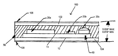
[0028] FIG. 2 shows a cross sectional view of an electronic inlay for an
electronic
card according to an embodiment of the present invention.
[0029] FIG. 3 shows a top view of a sheet of circuit boards for use in making
electronic inlays according to an embodiment of the present invention.
[0030] FIG. 4 shows a circuit board with circuit components attached to it
according
to an embodiment of the present invention.
[0031] FIG. 5 shows a schematic view of an electronic inlay with a nozzle used
to
inject thermosetting material between the top and bottom cover sheets.
[0032] FIG. 6 shows a cross sectional view of an assembly comprising an
electronic
inlay, a top overlay, and a bottom overlay in a laminator according to an
embodiment
of the present inverition.
[0033] FIG. 7 shows a cross sectional view of an electronic inlay for an
electronic
card according to an embodiment of the present invention.
-7-
CA 02648900 2008-10-08
WO 2007/126748 PCT/US2007/007446
DETAILED DESCRIPTION OF THE PREFERRED EMBODIMENTS
[0034] According to one embodiment of the present invention, as shown in FIG.
1, an
electronic card 1 may comprise an electronic inlay 100, a bottom overlay 30,
and a
top overlay 40. As seen in FIG. 2, the electronic inlay 100 may comprise a
circuit
board 10, a plurality of circuit components 20a-20c, a layer of thermosetting
material
50, a top cover sheet 102, and a lower cover sheet 104.
[0035] The circuit board 10 has a top surface 11 and a bottom surface 12.
According
to one embodiment of the invention, the circuit board 10 can be double-sided.
Accordingly, the circuit board 10 may be configured to accommodate a plurality
of
circuit traces 14 (shown in FIG. 3) on the top surface 11 and on the bottom
surface 12.
The circuit traces 14 are configured to operably connect the plurality of
circuit
components 20a-20c affixed to the circuit boarcl 10. The circuit traces 14
electrically
connect to the plurality of circuit components 20a-20c such that the circuit
components are capable of performing electrical functions within the
electronic card
1.
[0036] The circuit traces 14 may be provided upon the surfaces 11 and 12 of
the
circuit board in numerous ways. For example, the circuit traces 14 may be
formed on
the circuit board 10 with conductive ink. In the alternative, circuit traces
14 may be
etched onto the circuit board 10.
[0037] The circuit board 10 is comprised of any known conventional material
suitable
for receiving an electronic circuit. For example, the circuit board 10 may be
comprised of a flame retardant laminate with a woven glass reinforced epoxy
resin.
This material is also known as FR-4 board. Alternatively, the circuit board 10
may be
comprised of a plastic compound that is suitable for receiving conductive ink,
such as
polyester.
[0038] As shown in FIG. 2, and described below, the circuit board 10 is
configured to
receive and vertically stabilize a plurality of circuit components 20a-20c.
The
plurality of circuit components 20a-20c may be attached to the circuit board
10 and
specifically to the circuit traces 14 by any one of a number of methods. For
example,
-8-
CA 02648900 2008-10-08
WO 2007/126748 PCT/US2007/007446
in one embodiment of the invention, the circuit components 20a-20c are
connected to
the circuit board 10 with a conductive adhesive. Preferably, the plurality of
circuit
components are soldered onto the circuit board 10. The plurality of circuit
components 20a-20c can be positioned anywhere on the circuit board 10 as
desired.
The purpose of the electronic card 1 and the design parameters will dictate
the
position of the circuit traces 14 and the position of the circuit components
20a-20c.
Functionality will also dictate what types of circuit components 20a-20c
populate the
circuit board 10.
[00391 For example purposes only, the plurality of circuit components 20a-20c
could
be one of a battery, an LED, a button or switch. In addition, any one or all
of these
circuit components could populate the circuit board 10. Further, additional
circuit
components 20a-20c may include but are not limited to a microprocessor chip, a
speaker, a plurality of LEDs 26 (shown in FIG. 7), flexible displays, RFID
antennas
and emulators. Referring to FIG. 4, a circuit layout for an electronic inlay
100 is
shown. The circuit board 10 shown in FIG. 4 is populated by a battery 25, a
microprocessor 22, and a button 23. The electronic inlay 100 can include a
liquid
crystal display 24 as the circuit component connected to the button 23. The
liquid
crystal display 24 may be used to display information to a user, such as an
account
balance. In the alternative or in addition to, the electronic inlay 100 may
include a
speaker (not shown).
[0040] Generally, the components shown in FIG. 2 may vary in thickness and
length.
For example, the electronic inlay 100 can have a thickness of less than 0.03
inches.
However, the overall thickness of the electronic inlay 100 is preferably
between 0.016
and 0.028 inches. Accordingly, these dimensions allow the electronic inlay 100
to be
compatible with the conventional equipment used by different certified
financial card
houses to add the bottom overlay 30 and the top overlay 40. For example
purposes
only, the battery 25 can have a thickness of .016 inches, the push button 23
can have a
thickness of .020 inches and the microprocessor 22 has a thickness of .015
inches. In
addition, the electronic card 1 shown in FIG. 2 could have a speaker (not
shown)
having a thickness of .010 inches.
-9-
CA 02648900 2008-10-08
WO 2007/126748 PCT/US2007/007446
[0041] As shown in FIG. 2, a bottom cover sheet 104 is attached to the bottom
surface 12 of the circuit board 10. The bottom cover sheet 104 can be attached
to the
circuit board 10 by any number of known methods. Preferably, the bottom
surface 12
is attached to the bottom cover sheet 104 using a pressure sensitive adhesive
tape or a
spray-on adhesive. The bottom cover sheet 104 may be comprised of any suitable
material but preferably, the bottom cover sheet 104 is comprised of polyvinyl
chloride
(PVC), polyester, acrylonitrile-butadiene-styrene (ABS), polycarbonate,
polyethylene
terephthalate (PET), PETG, or any other suitable material. The bottom cover
sheet
104 can be, for example, 0.001 to 0.002 inches thick and can include a heat
seal
coating 106 on the outside of the cover sheet that is compatible with PVC. The
heat
seal coating 106 may be compatible with PVC since the bottom overlay 30 can be
made from PVC.
[0042] A top cover sheet 102 positioned above the top surface of the circuit
board 10
is shown in FIG. 2. The top cover sheet 102 may be comprised of any suitable
material, for example, the top cover sheet 102 may be polyvinyl chloride
(PVC),
polyester, acrylonitrile-butadiene-styrene (ABS), polycarbonate, polyethylene
terephthalate (PET), PETG, or any other suitable material. Like the bottom
cover
sheet, the top cover sheet can be, for example, 0.001 to 0.002 inches thick
and can
include a heat seal coating 106 on the outside of the cover sheet that is
compatible
with PVC. The heat seal coating 106 may be compatible with PVC since the top
overlay 40 can be made from PVC.
[0043] As previously mentioned, the overall thickness of the electronic inlay
100 can
vary as well as the thickness of the top 102 and bottom 104 cover sheets. In
addition
to the examples above, other examples can include electronic cards 1 having
thicknesses as low as 0.010 inches or lower and as high as 0.200 inches or
higher. In
addition, the top and bottom cover sheets can have thickness in the range of
0.010
inches to 0.200 inches. Thus, the overall thickness of the electronic inlay
100 and the
thicknesses of the individual parts, such as the top 102 and bottom 104 cover
sheets,
will depend on the particular application and desired dimensions of the
electronic card
1.
-10-
CA 02648900 2008-10-08
WO 2007/126748 PCT/US2007/007446
[0044] As shown in FIG. 2, a layer of thermosetting material 50 is positioned
between
the top surface of the circuit board 10 and the top cover sheet 102. In
addition, the
layer of thermosetting material 50 is present in an area below the bottom
surface 11 of
the circuit board 10 and above the bottom cover sheet 104. Preferably the
layer of
thermosetting material 50 is composed of a thermosetting polymeric material.
For
example, the layer of thermosetting material 50 can be composed of polyurea.
[0045] Polyurea is a known elastomer that is derived from the reaction product
of an
isocyanate component and a resin blend component. The isocyanate can be
aromatic
or aliphatic in nature. It can be a monomer, a polymer, or any variant
reaction of
isocyanates, quasi-prepolymer or a prepolymer. The prepolymer, or quasi-
prepolymer, can be made of an "amine-terminated polymer resin or a hydroxyl-
terminated polymer resin. The resin blend must be made up of amine-terminated
polymer resins, and/or amine-terminated chain extenders. The amine-terminated
polymer resins will not have any intentional hydroxyl moieties. Any hydroxyls
are
the result of an incomplete conversion to the amine-terminated polymer resins.
The
resin blend may also contain additives or non-primary components. These
additives
may contain hydroxyls, such as pre-dispersed pigments in a polyol carrier.
Normally,
the resin blend will not contain a catalyst(s).
[0046] Using a polyurea formulation, such as a pure polyurea, as the layer of
thermosetting material 50 allows the electronic inlay 100 to withstand the hot
lamination temperatures used in the hot lamination process when the top 102
and
bottom 104 overlays are added to the electronic inlay 100 to form
the.electronic card
1. Such hot lamination temperatures can include the range of 250 to 300 F.
[00471 According to another embodiment, the electronic inlay 100 does not
include a
bottom cover sheet 104 as shown in FIG. 7. A plurality of circuit components
20a-
20c are positioned on the circuit board 10. A top cover sheet 102 is
positioned above
the populated circuit board 10, wherein a layer of thermosetting material 50
is
positioned between the bottom surface of the top cover sheet 102 and the top
surface
of the circuit board 10. The circuit board 10 can include a PVC compatible
heat seal
coating 106 applied to the bottom surface 12 of the circuit board 10.
Preferably, the
-11-
CA 02648900 2008-10-08
WO 2007/126748 PCT/US2007/007446
heat seal coating 106 may be compatible with PVC since the bottom overlay 30
can
be made from PVC.
[0048] Once the injection of the layer of thermosetting material 50 is
complete and
the electronic inlay is ready for removal and shipping, the electronic inlay
may be
shipped to certified financial card houses, which will add the remaining top
overlay
40 and the bottom overlay 30.
[0049] The bottom overlay 30 can be attached to the bottom surface of the heat
seal
coating 106 if present. If there is no heat seal coating, the bottom overlay
30 can be
attached to the bottom surface of the bottom cover sheet 104 or the circuit
board 10.
If the heat seal coating 106 is used, it will facilitate the hot lamination
process for
attaching the bottom overlay 30 to the electronic inlay 100. The bottom
overlay 30
may be comprised of any suitable material but preferably, the bottom overlay
30 is
comprised of polyvinyl chloride (PVC) or like material. According to one
embodiment of the invention, the surface of the bottom overlay 30 in contact
with the
heat seal coating 106 and/or in contact witli the bottom cover sheet 104 or
circuit
board 10 has printed information. Alternatively, printed information may be
placed
on the outside surface of the bottom overlay 30. For example, the bottom
overlay 30
may include printed information consistent with a standard credit card,
including a
name, expiration date, and account number.
[0050] According to another embodiment of the invention, the bottom overlay 30
may
be clear or "2/5 clear/white printed." "2/5 clear/white printed" means that
the overlay
comprises a 0.005" printed white PVC layer with a 0.002" clear laminate over
the
printed surface of the 0.005" layer. Of course, other types of overlays can be
used
such as a printed white PVC layer that is less than 0.005" thick and/or a
clear laminate
layer that is less than 0.002" thick.
[0051] A top overlay 40 positioned above the top surface of the circuit board
10 is
shown in FIG 1. rThe top overlay 40 may be comprised of any suitable material,
for
example, the top overlay 40 may comprise of polyvinyl chloride (PVC) or like
material. According to one embodiment of the invention, the surface of the top
-12-
CA 02648900 2008-10-08
WO 2007/126748 PCT/US2007/007446
overlay 40 in contact with the layer of thermosetting material 50 has printed
information. Alternatively, the outside surface of the top overlay 40 may have
printed
information. For example, the top overlay 40 may include printed information
consistent with a standard credit card, including a name, expiration date and
account
number.
[0052] According to another embodiment of the invention, the top overlay 40
may be
clear or "2/5 clear/white printed," as discussed above. As with the bottom
overlay 30,
other types of overlays can be used such as a printed white PVC layer that is
less than
0.005" thick and/or a clear laminate layer that is less than 0.002" thick.
[0053] As previously mentioned, the overall dimensions of the electronic card
1 and
the electronic inlay 100 deserve special attention. In particular for the
purpose of
producing a financial card that meets ISO 07816 standards, the finished card
cannot
exceed 0.033 inches (or 0.76 mm) in thickness. Thus, the thicknesses of the
top
overlay 40, the bottom overlay 30, and the electronic inlay 100 cannot be
considered
independent of each other. For example, if the top 40 and bottom 30 overlays
both
comprise 2/5 clear/white printed, then each overlay is 0.007 inches thick.
Thus, the
electronic inlay's 100 thickness cannot exceed 0.019 inches. If, however, the
top 40
or the bottom 30 overlay is less than 0.007 inches thick, then the inlay's 100
thickness
can be higher as long as the combination of the thickness of the top overlay
40, the
bottom overlay 30, and the electronic inlay 100 do not exceed 0.033 inches.
[0054] Other variations of these arrangements are also contemplated. For
example,
instead of the use of a top cover sheet 102, a mold release could be utilized.
In such a
configuration, there would be circuit components disposed on a circuit board
10, the
circuit board 10 would be disposed on a bottom cover sheet 104, and a layer of
thermosetting material 50 disposed on the circuit components, the circuit
board 10,
and the bottom cover sheet 104. A mold release, such as a silicon spray, would
be
applied to the top of the mold to facilitate the separation of the electronic
inlay from
the mold. The mold release residue would be removed from the electronic inlay
before the hot lamination process to add on the top and bottom overlays takes
place.
-13-
CA 02648900 2008-10-08
WO 2007/126748 PCT/US2007/007446
[00551 A method for manufacturing an electronic card according to the present
invention will now be described.
[0056] First, a circuit board 10 is provided. The circuit board 10 has a top
surface 11
and a bottom surface 12. Circuit traces 14 are present on the top surface 11
of the
circuit board 10. Alternatively, the circuit board may be double-sided having
circuit
traces 14 on the top surface 11 and the bottom surface 12.
[00571 Next, a plurality of circuit components 20a-20c are then positioned
onto the
circuit board 10 and electrically connected to the circuit traces 14 on the
top and/or
bottom surface of the circuit board 10. The circuit components 20a-20c may be
connected by any one of several methods including the use of double-sided
electrically conducting tape. Preferably, the plurality of circuit components
20a-20c
are connected via a conventional soldering process.
[0058] Next, the bottom surface 12 of the circuit board 10 is affixed to the
bottom
cover sheet 104. Preferably, the bottom surface 12 is attached to the bottom
cover
sheet 104 using a pressure sensitive adhesive tape or a spray-on adhesive.
According
to another embodiment, the bottom surface 12 of the circuit board is not
attached to a
bottom cover sheet 104. In this embodiment, the circuit board functions as the
bottom
cover sheet 104.
[0059) The circuit board 10, with or without the bottom cover sheet 104 is
then
loaded as one complete sheet into an injection molding apparatus. A top cover
sheet
102 is placed into the.injection molding apparatus and positioned such that
the top
cover sheet 102 is above the top surface 11 of the circuit board 10.
Specifically, the
injection molding apparatus may be a reaction injection molding machine
{"which is
often individually referred to as "RIM"). These machines are associated with a
top
mold shell and a bottom mold shell that are capable of performing cold, low
pressure,
forming operations on at least one of the sheets of polymeric material (e.g.,
PVC) that
can make up the top cover sheet 102 and the bottom cover sheet 104. Such top
and
bottom mold shells cooperate in ways that are well known to those skilled in
the
polymeric material molding arts.
-14-
CA 02648900 2008-10-08
WO 2007/126748 PCT/US2007/007446
[0060] The injection molding apparatus then injects thermosetting polymeric
material
via a nozzle 60 (shown in FIG. 5) between the top cover sheet 102 and the
circuit
board 10/ bottom cover sheet 104, forming the layer of thermosetting material
50
from the thermosetting polymeric material. Preferably, as mentioned above, the
thermosetting polymeric material can be polyurea but other suitable materials
can be
used.
[0061] Cold, low pressure forming conditions generally mean forming conditions
wherein the temperature of the thermosetting polymeric material, is less than
the heat
distortion temperature of the top cover sheet 102 and the bottom cover sheet
104/
circuit board 10, and the pressure is less than about 500 psi. Preferably, the
cold
forming temperatures will be at least 100 F less than the heat distortion
temperature
of the top cover sheet 102 and the bottom cover sheet 104/ circuit board 10.
The heat
distortion temperature of many polyvinyl chloride (PVC) materials is about 230
F.
Thus, the temperatures used to cold form such PVC sheets in the present
invention
will be no more than about 130 F.
[0062] According to one embodiment of the invention, the more preferred cold,
low
pressure forming procedures will involve injection of thermosetting polymeric
materials with temperatures ranging from about 56 F to about 160 F, under
pressures that preferably range from about atmospheric pressure to about 500
psi. In
another embodiment of the invention, the temperatures of the thermosetting
polymeric
material being injected into the electronic inlay 100 will be between about 65
F and
about 70 F under injection pressures that preferably range from about 80 to
120 psi.
[0063] During the injection process, gates are used to allow the flow of the
thermosetting material between the top and bottom cover sheets. On the other
hand,
no runners are used in the process, which results in a sheet of electronic
inlays 100
that will be flat. It should also be noted that if the heat seal coating 106
on the top
102 and bottom cover sheets 104/ circuit board 10 is used, the coating can be
added at
any appropriate time in the process. For example, the heat seal coating can be
added
before the cover sheets are inserted into the mold or after the sheet of
electronic inlays
is removed from the mold.
-15-
CA 02648900 2008-10-08
WO 2007/126748 PCT/US2007/007446
[0064] After the injection of the thermosetting polymeric material, the molded
structure is then removed from the injection molded apparatus. According to
one
embodiment of the invention, several electronic inlays 100 are formed on one
molded
sheet. FIG. 3 depicts several electronic inlays formed on one sheet. According
to
other embodiments, the injected sheet can correspond to a single electronic
inlay 100,
a single strip or row of electronic inlays 100, or an array of electronic
inlays. For
example, the injected sheet can include three rows of seven electronic inlays,
which
can allow existing card manufacturers to produce electronic cards using their
existing
equipment and processes that they use today. The stiffness of the electronic
inlay 100
will depend upon the materials used in the composition of each of the
individual
components of the electronic inlay 100.
[0065] The sheet of the electronic inlays 100 is then removed. Next, a top 40
and
bottom 30 overlay is applied to the electronic inlay 100 to form an electronic
card/tag
1. For example, card manufacturers may receive the sheets of electronic inlays
100
and use a hot lamination process to attach the top 40 and bottom 30 overlays
to the
electronic inlay. The use of the heat seal coating can facilitate the hot
lamination
process to attach the overlays. In addition, the heat seal coating can be PVC
compatible in the instance where PVC material is used for top 40 and bottom 30
overlays. The hot lamination process can operate in the temperature range of
about
250 F to about 320 F. For this reason, pure polyurea may be desirable since
it can
withstand such temperatures.
[0066] An example of a hot lamination process that can be used is presented in
U.S.
Patent 5,817,207, which is incorporated by reference herein. An example of
such a
process is presented in FIG. 6. In this -example, the sheet of electronic
inlays 202 is
placed between the top and bottom overlays 40 and 30. These layers are placed
in a
laminator 204 of the type well known in the art of plastic card manufacturing.
The
laminator 204 includes upper and lower platens 206 and 208 for applying ram
pressure to an article positioned therebetween. In addition to the ability to
apply ram
pressure, the controlled platens 206 and 208 may provide both heat and chill
cycles
and can include a cycle timer to regulate cycle time. The sheet of inlays 202
and the
-16-
CA 02648900 2008-10-08
WO 2007/126748 PCT/US2007/007446
top and bottom overlays 40 and 30 form an assembly 222 that is positioned
between
the first and second laminating plates 210 and 212, one of which can have a
matte
finish to provide at least one textured outer surface to either the top or
bottom overlay.
In addition, there are first and second laminating pads 214 and 216 positioned
outside
of the laminating plates 210 and 212 and first and second steel plates 218 and
220
positioned outside of the laminating pads 2,14 and 216. The assembly 222 is
shown to
be in position between platens 206 and 208 in FIG. 6.
[0067] Once the assembly 222 is in position in the laminator 204, the first
lamination
cycle is initiated by closing the platens 206 and 208, preferably applying
little or no
ram pressure to the assembly 222. A heat cycle is initiated, bringing the
temperature
of the platens 206 and 208 up to a range of 250 F to 320 F for a period of
greater
than 5 minutes, and preferably in the range of 7 to 10 minutes. Once the heat
cycle
has been applied to the assembly as is set forth above, the ram pressure of
the
laminator 40 is increased to facilitate the attachment of the top and bottom
overlays
40 and 30 to the electronic inlays. The ram pressure applied during the heat
cycle and
the length of the heat cycle may vary, depending especially upon the size of
the sheet
of the electronic inlays 202. For example, the cycle time may be in the range
of 10-15
minutes.
[0068] Subsequent to the above heat cycle, the laminator 204 applies a chill
cycle to
the assembly 222 during which time the ram pressure of the laminator 204 is
increased, preferably by approximately 25% until the platens 206 and 208 have
cooled to approximately 40 F to 65 F for approximately 10-15 minutes. The
finished assembly 222 may then be removed from the laminator 204 for
additional
processing.
[0069] After the assembly 222 is removed from the laminator 204, the assembly
can
have a layer of printing ink applied to either the top overlay, the bottom
overlay, or
both. This may be accomplished using a wide variety of printing techniques
such as
offset printing, letterpress printing, screen printing, roller coating, spray
printing,
litho-printing, and other suitable printing techniques. In addition, after the
top and
-17-
CA 02648900 2008-10-08
WO 2007/126748 PCT/US2007/007446
bottom overlays are applied to the electronic overlay sheet, the sheet can be
cut to
form individual electronic cards.
[0070] From the disclosure of the present application, it is possible to
provide an '
electronic inlay for the production of electronic cards in which the
application of
overlays onto the electronic inlays can be accomplished with existing
equipment used
in the industry today. Thus, a company that produces credit cards, for
example, can
easily make electronic cards in a more cost effective manner since there is a
reduction
in equipment costs.
[0071) Given the disclosure of the present invention, one versed in the art
would
appreciate that there may be other embodiments and modifications within the
scope
and spirit of the invention. Accordingly, all modifications attainable by one
versed in
the art from the present disclosure within the scope and spirit of the present
invention
are to be included as further embodiments of the present intention. The scope
of the
present invention is to be defined as set forth in the following claims.
-18-