Note: Descriptions are shown in the official language in which they were submitted.
CA 02667852 2009-04-28
SEMICONDUCTOR ELECTRONIC COMPONENT AND SEMICONDUCTOR
DEVICE USING THE SAME
TECHNICAL FIELD
The present invention relates to a chip-on-chip type semiconductor electronic
component and a semiconductor device comprising the same. More specifically,
the
present invention relates to a semiconductor electronic component which can
meet the
requirements for density increase of semiconductor integrated circuits and a
semiconductor device comprising the same.
BACKGROUND ART
Recently, as the need for sophistication and miniaturization of electronic
devices has been increased, the technique for high-density package of
semiconductor
integrated circuits has been developed. One example of such packaging
techniques is
a chip-on-chip type System in Package (SiP) in which a semiconductor chip is
mounted
on another semiconductor chip face down. Attention is focused on this
structure
because it allows thickness reduction of packages and is excellent in
reliability of
electrical connection.
In general, in a chip-on-chip type SiP, connection between semiconductor chips
is provided via fine bumps according to a flip-chip method. In this case, in
order to
ensure electrical connection strength and mechanical connection strength, a
filling resin
is injected into the position between the semiconductor chips (underfill
filling).
However, in this step of underfill filling, the filling resin injected between
the
semiconductor chips bleeds and an external electrode provided on the surface
of the
lower semiconductor chip is contaminated thereby, and for this reason, there
is a
problem that it is impossible to perform wire bonding. Therefore, the distance
between the side surface of the upper semiconductor chip and the external
electrode
provided on the lower semiconductor chip must be about 1.5 cm. Moreover, since
an
adhesive is injected between semiconductor chips, the chip gap must be at
least about
m. These requirements interrupt high-density package of semiconductor
35 integrated circuits.
Methods in which electrical connection and filling between semiconductor
chips are performed together via an anisotropic conductive film are also
known. For
example, Japanese Laid-Open Patent Publication No. 61-276873 (Patent Document
1)
describes an adhesion tape including solder particles. The document describes
a
40 method in which the adhesion tape is interposed between members to be
subjected to
1
CA 02667852 2009-04-28
thermocompression bonding, and thereby solder particles are interposed between
electrical connection portions of the members and other portions are filled
with a resin
component. Further, Japanese Patent No. 3769688 (Patent Document 2) describes
a
method of connecting terminals using an electrically conductive adhesive
including
electrically conductive particles and a resin component which is not
completely cured at
the meting point of the electrically conductive particles.
However, none of these methods realized further improvement of density
increase of semiconductor integrated circuits in chip-on-chip type SiPs.
DISCLOSURE OF THE 1NVENTION
Under the above-described circumstances, the development of a chip-on-chip
type semiconductor electronic component and a semiconductor device which can
meet
the requirements for further density increase of semiconductor integrated
circuits is
desired.
The present inventors diligently made researches in consideration of the
above-described problems of the conventional techniques, and successfully
performed
electrical connection and filling between semiconductor chips together by
minimizing
bleeding of a resin component at the time of meltdown of an adhesion film.
Thus, a
chip-on-chip type semiconductor electronic component and a semiconductor
device
which can meet the requirements for further density increase were successfully
obtained.
That is, the present invention provides a semiconductor electronic component,
a semiconductor device comprising the semiconductor electronic component and
the
like as follows:
[1] A chip-on-chip type semiconductor electronic component, which comprises: a
first
semiconductor chip having a circuit surface on which first internal electrodes
and first
external electrodes are provided; and a second semiconductor chip having a
circuit
surface on which second internal electrodes electrically connected to the
first internal
electrodes are provided, wherein the circuit surface of the first
semiconductor chip and
the circuit surface of the second semiconductor chip are opposed to each
other, and
wherein:
the gap between the first semiconductor chip and the second semiconductor
chip is filled with an insulating resin;
the distance between the first semiconductor chip and the second
semiconductor chip is 50 m or less; and
the shortest distance between the side surface of the second semiconductor
chip
and the first external electrode is 1 mm or less.
[2] A chip-on-chip type semiconductor electronic component, which comprises: a
first
2
CA 02667852 2009-04-28
semiconductor chip having a circuit surface on which first internal electrodes
and first
external electrodes are provided; and a second semiconductor chip having a
circuit
surface on which second internal electrodes electrically connected to the
first internal
electrodes are provided, wherein the circuit surface of the first
semiconductor chip and
the circuit surface of the second semiconductor chip are opposed to each
other, and
wherein:
the gap between the first semiconductor chip and the second semiconductor
chip is filled with an insulating resin;
the distance between the first semiconductor chip and the second
semiconductor chip is 25 m or less; and
the shortest distance between the side surface of the second semiconductor
chip
and the first external electrode is 1 mm or less.
[3] The semiconductor electronic component according to item [1] or [2],
wherein the
shortest distance between the first internal electrodes adjacent to each other
is 50 m or
less.
[4] The semiconductor electronic component according to any one of items [1]
to [3],
wherein the second semiconductor chip is provided on an approximate center
area of the
first semiconductor chip.
[5] The semiconductor electronic component according to any one of items [1]
to [4],
wherein the first external electrodes are provided on the marginal portion of
the first
semiconductor chip.
[6] The semiconductor electronic component according to any one of items [1]
to [5],
wherein: between the first semiconductor chip and the second semiconductor
chip,
solder bumps provided on at least either one of the first internal electrodes
and the
second internal electrodes and a thermosetting adhesive film comprising a flux
compound are interposed to be heat-sealed, and thereby the first internal
electrodes and
the second internal electrodes are electrically connected to each other; and
the gap
between the first semiconductor chip and the second semiconductor chip is
filled with
the insulating resin.
[7] The semiconductor electronic component according to item [6], wherein the
thermosetting adhesive film comprises 10 to 50 wt% of film forming resin, 30
to 80
wt% of curable resin and 1 to 20 wt% of curing agent having flux activity.
[8] The semiconductor electronic component according to item [7], wherein the
film
forming resin is at least one substance selected from the group consisting of
(meth)acrylic resin, phenoxy resin and polyimide resin.
[9] The semiconductor electronic component according to item [7] or [8],
wherein the
curable resin is epoxy resin.
[10] The semiconductor electronic component according to any one of items [7]
to [9],
wherein the curing agent having flux activity is at least one substance
selected from the
group consisting of aliphatic dicarboxylic acid and compounds having a
carboxyl group
3
CA 02667852 2009-04-28
and a phenolic hydroxyl group.
[ 11 ] The semiconductor electronic component according to any one of items
[6] to [ 10],
wherein, in the case where a tin-containing solder ball having the diameter of
500 m is
provided on the thermosetting adhesive film and heated at a temperature which
is 30 C
higher than the melting point of the solder ball for 20 seconds, the solder
wet-spreading
ratio of the thermosetting adhesive film represented by the following formula
(I) is 40%
or higher:
Solder wet-spreading ratio (%) = [{(diameter of solder ball) - (thickness of
solder after
wet spreading)}/(diameter of solder ball)] X 100 (I)
[ 12] The semiconductor electronic component according to any one of items [6]
to [ 11 ],
wherein, in the case where the thickness of the thermosetting adhesive film is
100 m,
the melt viscosity thereof at 223 C is 10 Pa- s to 200000 Pa- s.
[13] The semiconductor electronic component according to any one of items [1]
to [5],
wherein: between the first semiconductor chip and the second semiconductor
chip, a
thermosetting adhesive film comprising solder powder and a flux compound is
interposed to be heat-sealed, and thereby the first internal electrodes and
the second
internal electrodes are electrically connected to each other; and the gap
between the first
semiconductor chip and the second semiconductor chip is filled with the
insulating
resin.
[14] The semiconductor electronic component according to item [13], wherein
constituents other than the solder powder in the thermosetting adhesive film
comprise
10 to 50 wt% of film forming resin, 30 to 80 wt% of curable resin and 1 to 20
wt% of
curing agent having flux activity.
[15] The semiconductor electronic component according to item [13] or [14],
wherein
the thermosetting adhesive film comprises 30 to 200 parts by weight of solder
powder
per 100 parts by weight of constituents other than the solder powder.
[16] The semiconductor electronic component according to item [14] or [15],
wherein
the film forming resin is at least one substance selected from the group
consisting of
(meth)acrylic resin, phenoxy resin and polyimide resin.
[17] The semiconductor electronic component according to any one of items [14]
to
[16], wherein the curable resin is epoxy resin.
[18] The semiconductor electronic component according to any one of items [14]
to
[17], wherein the curing agent having flux activity is at least one substance
selected
from the group consisting of aliphatic dicarboxylic acid and compounds having
a
carboxyl group and a phenolic hydroxyl group.
[19] The semiconductor electronic component according to any one of items [13]
to
[18], wherein a curing temperature T1 of the thermosetting adhesive film and a
melting
point T2 of the solder powder satisfy the following formula (II):
T1 > T2 + 20 C (II)
and the melt viscosity of the thermosetting adhesive film at the melting point
T2 of the
4
CA 02667852 2009-04-28
solder powder is 50 Pa = s to 5000 Pa = s.
[20] The semiconductor electronic component according to any one of items [13]
to
[19], wherein, in the case where the thickness of the thermosetting adhesive
film is 100
m, the melt viscosity thereof at 138 C is 1 Pa= s to 10000 Pa= s.
[21] The semiconductor electronic component according to any one of items [1]
to [20],
wherein a semiconductor chip is further provided on a surface opposite to the
circuit
surface of the second semiconductor chip.
[22] The semiconductor electronic component according to any one of items [ 1]
to [21 ],
further comprising a third semiconductor chip having a circuit surface on
which a third
internal electrode is provided, wherein:
the circuit surface of the third semiconductor chip is opposed to the surface
opposite to the circuit surface of the second semiconductor chip;
the gap between the second semiconductor chip and the third semiconductor
chip is filled with the insulating resin; and
the third internal electrode is electrically connected to the second internal
electrode via through-holes provided in the thickness direction of the second
semiconductor chip.
[23] A semiconductor device on which the semiconductor electronic component
according to any one of items [ 1] to [22] is mounted.
The present invention can provide a semiconductor electronic component in
which the distance between semiconductor chips is 50 m or less, and
preferably 25 m
or less. By using the semiconductor electronic component of the present
invention, the
total thickness of the whole component to be packaged in a semiconductor
device can
be reduced, and the weight of the whole component to be packaged can also be
reduced.
The present invention can also provide a semiconductor electronic component
in which the shortest distance between the side surface of the upper
semiconductor chip
and an external electrode provided on the lower semiconductor chip is 1 mm or
less.
By using the semiconductor electronic component of the present invention, the
integration density of semiconductor chips, which one package can include, can
be
increased. Further, the whole component to be packaged can be miniaturized.
Moreover, according to a preferred embodiment of the present invention, the
present invention can provide a semiconductor electronic component in which
the
shortest distance between internal electrodes provided on the surface of a
semiconductor
chip is 50 m or less. By using the semiconductor electronic component of the
present
invention, the amount of information, which one package can include, can be
increased.
According to a preferred embodiment of the present invention, the present
invention can provide a multiple-layer stack type semiconductor electronic
component
in which a plurality of semiconductor chips are stacked. According to a
preferred
embodiment of the present invention, in the multiple-layer stack type
semiconductor
electronic component of the present invention, the distance between
semiconductor
5
CA 02667852 2009-04-28
chips is 50 m or less, and preferably 25 m or less, and the shortest
distance between
the side surface of the upper semiconductor chip and an external electrode
provided on
the lower semiconductor chip is 1 mm or less. Further, according to a
preferred
embodiment of the present invention, in the multiple-layer stack type
semiconductor
electronic component of the present invention, the shortest distance between
internal
electrodes provided on the surface of a semiconductor chip is 50 m or less.
By using
the above-described semiconductor electronic component of the present
invention, the
integration density of semiconductor chips, which one package can include, can
be
further increased.
Furthermore, the present invention can provide a semiconductor device in
which the semiconductor electronic component of the present invention is
mounted on a
substrate. The semiconductor device of the present invention meets
requirements for
sophistication and miniaturization of electronic devices since it allows
increase of the
integration density of semiconductor chips which one package can include.
BRIEF DESCRIPTION OF THE DRAWINGS
FIG 1 shows a schematic top view and a schematic cross sectional view of a
semiconductor electronic component according to one embodiment of the present
invention.
FIG 2 shows a schematic cross sectional view of a multiple-layer stack type
semiconductor electronic component according to one embodiment of the present
invention.
FIG 3 shows explanatory drawings for steps in a method for producing a
semiconductor electronic component according to one embodiment of the present
invention.
FIG 4 shows explanatory drawings for steps in a method for producing a
semiconductor electronic component according to one embodiment of the present
invention.
FIG 5 shows a schematic cross sectional view of a semiconductor device
according to one embodiment of the present invention.
FIG 6 shows a schematic cross sectional view of a multiple-layer stack type
semiconductor device according to one embodiment of the present invention.
FIG 7 shows an explanatory drawing for steps in a method for producing the
semiconductor electronic component of the Examples of the present invention.
FIG 8 shows an explanatory drawing for steps in a method for producing the
semiconductor electronic component of the Examples of the present invention.
6
CA 02667852 2009-04-28
EXPLANATIONS OF LETTERS OR NUMERALS
1 semiconductor electronic component
2 multiple-layer stack type semiconductor electronic component
10 first semiconductor chip
20 second semiconductor chip
30 third semiconductor chip
11 first internal electrode
12 external electrode
20a side surface of second semiconductor chip
21 second internal electrode
30a side surface of third semiconductor chip
31 third internal electrode
100 solder area
101 insulating area
102 through-hole
103 UBM layer
104 UBM layer
105 solder bump
106 thermosetting adhesive film
107 protecting layer
108 thermosetting adhesive film
108a solder powder
109 circuit board
110 wire
111 encapsulating resin
112 bump electrode
113 passivating layer
114 thermally-oxidized film
BEST MODE FOR CARRYING OUT THE INVENTION
Hereinafter, preferred embodiments of the present invention will be described
by way of examples.
1. Semiconductor electronic component
Firstly, a semiconductor electronic component according to one embodiment of
the present invention will be described with reference to Figure 1.
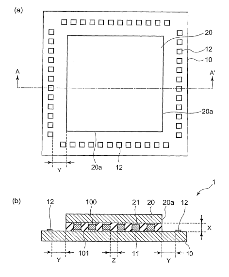
Figure 1(a) is a schematic top view of a semiconductor electronic component
7
CA 02667852 2009-04-28
according to one embodiment of the present invention. Figure 1(b) is a
schematic
cross sectional view taken along line A-A' in Figure 1(a). In Figure 1(b), the
semiconductor electronic component 1 according to the embodiment has a
structure in
which a circuit surface (not shown) of a first semiconductor chip 10 on which
internal
electrodes 11 are provided is opposed to a circuit surface (not shown) of a
second
semiconductor chip 20 on which internal electrodes 21 are provided. As shown
in
Figure 1(b), the internal electrodes 11 are patterned to correspond to the
internal
electrodes 21, and a solder area 100 is formed between each internal electrode
11 and
each internal electrode 21 which are opposed to each other. Two opposed
internal
electrodes are electrically connected to each other via the solder area 100.
Further, the
gap between the semiconductor chip 10 and the semiconductor chip 20 is filled
with an
insulating resin to form an insulating resin area 101, by which internal
electrodes
adjacent to each other are electrically insulated. On the circuit surface of
the
semiconductor chip 10, external electrodes 12 for connecting an integrated
circuit (not
shown) formed on the circuit surface of the semiconductor chip 10 to a circuit
board
made of silicon or the like are provided.
The distance X between the semiconductor chip 10 and the semiconductor chip
is 50 m or less, preferably 25 m or less, more preferably 5 m or less, and
even
more preferably 3 m or less. When producing the semiconductor electronic
20 component of the present invention using the production method according to
the first
embodiment of the present invention described later, the distance X depends on
the size
of a solder ball. For example, when using a solder ball having the diameter of
50 m,
the distance X is preferably 35 to 48 m, and more preferably 40 to 45 m.
When
producing the semiconductor electronic component of the present invention
using the
production method according to the second embodiment of the present invention
described later, the distance X is preferably 5 m or less, and more
preferably 3 m or
less. In this regard, the distance X refers to the distance between the
circuit surface of
the semiconductor chip 10 and the circuit surface of the semiconductor chip
20. From
the viewpoint of ensuring the connection strength between the semiconductor
chips, the
distance X is preferably 1 m or more.
Further, the shortest distance Y between the side surface 20a of the
semiconductor chip 20 and the external electrode 12 provided on the circuit
surface of
the semiconductor chip 10 is 1 mm or less, preferably 0.7 mm or less, and more
preferably 0.5 mm or less. In order to maintain a space for wire bonding, the
shortest
distance Y is generally 0.05 mm or more, but the present invention is not
particularly
limited thereto. In the expression "the shortest distance Y between the side
surface 20a
of the semiconductor chip 20 and the external electrode 12 provided on the
semiconductor chip 10", the term "shortest" is purposely used in order to
express a
distance between points which are closest to each other in the case where the
distance
between the side surface 20a of the semiconductor chip 20 and the external
electrode 12
8
CA 02667852 2009-04-28
provided on the circuit surface of the semiconductor chip 10 is not fixed.
Moreover, the shortest distance Z between the internal electrodes adjacent to
each other (a plurality of internal electrodes are provided on the circuit
surface of the
semiconductor chip) is preferably 50 m or less, more preferably 30 m or
less, and
even more preferably 20 m or less. From the viewpoint of ensuring the
electrical
connection reliability, the shortest distance Z is preferably 10 to 30 m. In
the
expression "the shortest distance Z between the internal electrodes adjacent
to each
other (a plurality of internal electrodes are provided on the semiconductor
chip)", the
term "shortest" is purposely used in order to express a distance between
points which
are closest to each other in the case where the distance Z between the
internal electrodes
which are adjacent to each other is not fixed.
The size of the first semiconductor chip 10 is preferably larger than that of
the
second semiconductor chip 20, but the present invention is not particularly
limited
thereto. From the viewpoint of improving the integration density of the
semiconductor
chips, as shown in Figure 1(a), the semiconductor chip 20 is preferably
provided on the
approximate center area of the semiconductor chip 10. Further, the external
electrode
12 which is provided on the semiconductor chip 10 is preferably provided on
the
marginal portion of the semiconductor chip 10.
The solder area 100 is an area in which a solder component is melted and
fixed.
The opposed internal electrodes are conducted via this area. The solder
component to
be used for the solder area 100 is not particularly limited, but for example,
it is
preferably an alloy comprising at least two substances selected from the group
consisting of tin (Sn), silver (Ag), bismuth (Bi), indium (In), zinc (Zn) and
copper (Cu).
The use amount of the solder component to be used for the solder area 100 is
not
particularly limited as long as it is within the range in which the opposed
internal
electrodes can be conducted.
The insulating area 101 is an area filled with an insulating resin. The
internal
electrodes which are adjacent to each other are electrically insulated by this
area. The
insulating resin to be used for the insulating area 101 is preferably a
curable resin from
the viewpoint of enhancing the electrical connection strength and the
mechanical
adhesive strength. The use amount of the insulating resin to be used for the
insulating
area 101 is not particularly limited as long as it is within the range in
which the internal
electrodes which are adjacent to each other can be electrically insulated.
Materials, etc. to be used for the solder area 100 and the insulating area 101
will be described in detail in the item related to production method described
later.
The thickness of each of the semiconductor chips 10 and 20 is preferably 10 to
1000 m, and more preferably 750 m or less, but the present invention is not
particularly limited thereto. Further, the size and materials of the internal
electrodes
and external electrodes are not particularly limited, and can be suitably
selected
depending on the intended use. Regarding the semiconductor chips, internal
electrodes,
9
CA 02667852 2009-04-28
external electrodes, etc. to be used in the present invention, for example,
the following
descriptions can be referred to: "CSP-gijutsu No Subete Part 2 (All about CSP
Technique Part 2)", written by Eiji Hagimoto, published by Kogyo Chosakai
Publishing,
Inc., pp. 62-72, 84-88 and 39-60; "SiP-gijutsu No Subete (All about SiP
Technique)",
written by Takashi Akazawa, published by Kogyo Chosakai Publishing, pp. 176-
188
and 192-205; and Japanese Laid-Open Patent Publication No. 2004-63753.
Since this embodiment has the above-described constitution, the whole
component to be packaged can be subjected to thickness and size reduction, and
moreover, the whole component to be packaged can also be subjected to weight
reduction.
In the present invention, a multiple-layer stack type semiconductor electronic
component in which a semiconductor electronic component 1 is further laminated
with
other semiconductors may be constituted. Figure 2 shows a schematic cross
sectional
view of a multiple-layer stack type semiconductor electronic component
according to
one embodiment of the present invention.
As shown in Figure 2, on the surface opposite to the circuit surface of the
semiconductor chip 20 on which the internal electrodes 21 are provided, a
semiconductor chip 30 on which internal electrodes 31 are provided is provided
to
constitute a multiple-layer stack type semiconductor electronic component 2.
The internal electrodes 31 which are provided on the circuit surface of the
semiconductor chip 30 are conducted to the circuit surface of the
semiconductor chip 20
by the solder area 100 via through-holes 102 provided in the thickness
direction of the
semiconductor chip 20, and are electrically connected to the internal
electrodes 21 on
the semiconductor chip 20. In this regard, the through-holes 102 are formed,
for
example, by forming through holes in the thickness direction of the
semiconductor chip
20 by means of drilling or the like, applying plating to inner wall surfaces
of the through
holes and filling the plated through holes with resin. Regarding through
holes, for
example, the following descriptions can be referred to: Japanese Laid-Open
Patent
Publication No. 2001-127243; and Japanese Laid-Open Patent Publication No.
2002-026241. The gap between the semiconductor chip 20 and the semiconductor
chip 30 is filled with an insulating resin to form an insulating area 101. By
the
insulating area 101, internal electrodes which are adjacent to each other are
electrically
insulated.
Thus, according to this embodiment, semiconductor chips can be mounted in a
multiple-layer form. The distance between the semiconductor chip 20 and the
semiconductor chip 30 is preferably within the same range as that of the
distance X
between the semiconductor chip 10 and the semiconductor chip 20, but the
present
invention is not particularly limited thereto. Further, the shortest distance
between the
side surface 30a of the semiconductor chip 30 and the external electrode 12
provided on
the circuit surface of the semiconductor chip 10 is preferably within the same
range as
CA 02667852 2009-04-28
that of the shortest distance Y between the side surface 20a of the
semiconductor chip
20 and the external electrode 12 provided on the circuit surface of the
semiconductor
chip 10. Moreover, the shortest distance between the internal electrodes
adjacent to
each other (a plurality of internal electrodes are provided on the circuit
surface of the
semiconductor chip 30) is preferably within the same range as that of the
shortest
distance Z between the internal electrodes adjacent to each other provided on
the circuit
surface of the semiconductor chip 10 or 20.
2. Method for producing a semiconductor electronic component
Next, a method for producing a semiconductor electronic component according
to one embodiment of the present invention will be described with reference to
Figures
3 and 4. Figure 3 shows explanatory drawings for steps in a method for
producing a
semiconductor electronic component according to one embodiment of the present
invention (the first embodiment), and Figure 4 shows explanatory drawings for
steps in
a method for producing a semiconductor electronic component according to
another
embodiment of the present invention (the second embodiment).
(1) First embodiment
Firstly, a method of producing a semiconductor electronic component
according to the first embodiment of the present invention will be described
with
reference to Figure 3.
As shown in Figure 3(a), firstly, a semiconductor chip 10 in which an internal
electrode I1 is provided on a circuit surface thereof and a semiconductor chip
20 in
which an internal electrode 21 is provided on a circuit surface thereof are
prepared. In
order to obtain good electrical connection, surfaces of the internal
electrodes 11 and 21
may be subjected to treatment such as washing, polishing, plating and surface
activation
in advance. For example, as shown in Figure 3(a), UBM (Under Barrier Metal)
layers
103 and 104 may be formed on the surfaces of the internal electrodes 11 and 21
using Ti,
Ti/Cu, Cu, Ni, Cr/Ni or the like. One or more LTBM layers may be formed. The
surfaces of the semiconductor chips 10 and 20 may be subjected to surface
stabilization
treatment in advance for the purpose of protecting a semiconductor element.
For
example, a passivating layer 113 (e.g., SiN film) may be formed. Further, as a
layer
for releasing residual stress present in the joint portion between a solder
bump and the
UBM layer and the internal electrode, an organic resin protecting layer such
as a
polyimide film, a polybenzooxazol film and a benzocyclobutene film may be
formed
(not shown).
Next, as shown in Figure 3(b), a solder bump 105 is formed on at least one of
the internal electrodes 11 and 21. The solder bump 105 may be formed by means
of a
plating method or a solder paste printing method. In Figure 3(a), the solder
bump 105
is formed on the internal electrode 21, but it may be formed only on the
internal
11
CA 02667852 2009-04-28
electrode 11, and it may be formed on both the internal electrodes 11 and 21.
The
solder bump 105 may be subjected to reflow process after it is formed.
A solder component constituting the solder bump 105 is preferably an alloy
comprising at least two substances selected from the group consisting of tin
(Sn), silver
(Ag), bismuth (Bi), indium (In), zinc (Zn) and copper (Cu). Among these
substances,
alloys containing Sn such as Sn-Bi alloy, Sn-Ag-Cu alloy and Sn-In alloy are
preferred
in view of melting temperature and mechanical properties. The melting point of
the
solder bump is generally 100 C or higher, and preferably 130 C or higher from
the
viewpoint of ensuring sufficient flowability of a resin component in a
thermosetting
adhesive film. Further, the melting temperature of the solder bump is
generally 250 C
or lower, and preferably 230 C or lower from the viewpoint of preventing heat
deterioration of an element provided on a circuit board or a semiconductor
chip at the
time of adhesion. An endothermic peak temperature, which is obtained when
measuring solder powder alone constituting the solder bump with the rate of
temperature increase of 10 C/min using DSC or the like, is regarded as the
melting
point of the solder bump.
Regarding the size of the solder bump 105, the diameter thereof is preferably
5
to 500 m, more preferably 10 to 300 m, and even more preferably 20 to 200 m
from
the viewpoint of ensuring sufficient electrical connection reliability.
Next, as shown in Figure 3(c), a thermosetting adhesive film 106 comprising a
flux compound is interposed between the semiconductor chip 10 and the
semiconductor
chip 20, and it is heated to a temperature at which curing of the
thermosetting adhesive
film 106 is not completed and the solder bump 105 is melted. By heating, the
solder
component constituting the solder bump 105 is melted, and the melted solder
component is aggregated on the surface of the internal electrode. Further, the
surface
of the internal electrode and the solder component are joined together to form
a solder
area 100, and thereby internal electrodes opposed to each other are
electrically
connected.
When the thickness of the thermosetting adhesive film is set as 100 m, the
melt viscosity of the thermosetting adhesive film at the melting point of the
solder bump
is preferably 50 to 5000 Pa = s, and more preferably 100 to 4000 Pa = s. When
the melt
viscosity of the thermosetting adhesive film at the melting point of the
solder bump is
within the above-described range, diffusion of the solder component between
the
internal electrodes can be suppressed, and bleeding of the resin component can
be
suppressed. For the purpose of preventing heat deterioration of the
semiconductor
electronic component, the curing temperature of the thermosetting adhesive
film is
preferably lower than 250 C. The melt viscosity of the thermosetting adhesive
film
can be measured using a sample in which the thickness of the adhesive film is
100 m
and a dynamic viscoelasticity measurement apparatus with the frequency of 0. 1
Hz and
the rate of temperature increase of 10 C/min.
12
CA 02667852 2009-04-28
At the time point when the heating temperature reaches the melting point of
the
solder bump, the distance between the internal electrodes opposed to each
other may be
decreased by applying pressure on the semiconductor chips 10 and 20.
Thus, the solder component melted by heating is aggregated between the
internal electrodes opposed to each other and is fixed to form the solder area
100 as
shown in Figure 3(c), and thereby the internal electrodes opposed to each
other are
electrically connected. Meanwhile, the gap between the semiconductor chip 10
and
the semiconductor chip 20 is filled with a resin component contained in the
thermosetting adhesive film 106, and thus the resin component forms an
insulating area
101. The internal electrodes adjacent to each other are electrically insulated
by the
insulating area 101.
Next, the resin component of the thermosetting adhesive film 106 is completely
cured to ensure electrical connection strength and mechanical adhesive
strength.
According to this embodiment, the internal electrodes opposed to each other
are
electrically connected in this way, and the gap between the semiconductor chip
10 and
the semiconductor chip 20 can be sealed with the insulating resin.
(a) Flux compound
In this regard, the thermosetting adhesive film 106 includes a flux compound.
In the resin component, the flux compound efficiently moves to the interface
between
the internal electrode and the solder bump. The flux compound removes an
oxidized
film on the surface of the solder bump 105, and thereby wettability of the
solder bump
can be improved. As a result, the connection resistance value between the
internal
electrodes opposed to each other can be reduced. When using such a flux
compound,
the step of washing flux can be omitted. As a result, the manufacturing
process can be
simplified.
Examples of flux compounds include compounds comprising a phenolic
hydroxyl group or a carboxyl group, etc.
Examples of phenolic hydroxyl group-containing compounds include:
monomers containing a phenolic hydroxyl group such as phenol, o-cresol, 2,6-
xylenol,
p-cresol, m-cresol, o-ethylphenol, 2,4-xylenol, 2,5-xylenol, m-ethylphenol,
2,3-xylenol,
mesitol, 3,5-xylenol, p-tertiary butyl phenol, catechol, p-tertiary
amylphenol, resorcinol,
p-octylphenol, p-phenylphenol, bisphenol F, bisphenol F, bisphenol AF,
biphenol, diallyl
bisphenol F, diallyl bisphenol A, trisphenol and tetrakisphenol; phenol
novolac resin;
o-cresol novolac resin; bisphenol F novolac resin; and bisphenol A novolac
resin.
Examples of carboxyl group-containing compounds include aliphatic acid
anhydride, alicyclic acid anhydride, aromatic acid anhydride, aliphatic
carboxylic acid,
aromatic carboxylic acid and phenols.
Examples of aliphatic acid anhydrides include succinic anhydride, polyadipic
acid anhydride, polyazelaic acid anhydride and polysebacic acid anhydride.
13
CA 02667852 2009-04-28
Examples of alicyclic acid anhydrides include methyltetrahydrophthalic
anhydride, methylhexahydrophthalic anhydride, methyl himic anhydride,
hexahydrophthalic anhydride, tetrahydrophthalic anhydride,
trialkyltetrahydrophthalic
anhydride, and methylcyclohexenedicarboxylic anhydride.
Examples of aromatic acid anhydrides include phthalic anhydride, trimellitic
anhydride, pyromellitic anhydride, benzophenone tetracarboxylic anhydride,
ethylene
glycol bistrimellitate and glycerol tristrimellitate.
Examples of aliphatic carboxylic acids include formic acid, acetic acid,
propionic acid, butyric acid, valeric acid, pivalic acid, caproic acid,
caprylic acid, lauric
acid, myristic acid, palmitic acid, stearic acid, acrylic acid, methacrylic
acid, crotonic
acid, oleic acid, fumaric acid, maleic acid, oxalic acid, malonic acid,
succinic acid,
glutaric acid, adipic acid, sebacic acid, dodecanedione acid, and pimelic
acid. Among
the above-described substances, aliphatic carboxylic acids represented by
HOOC-(CH2)p COOH (n is an integer from 0 to 20) are preferred. For example,
adipic acid, sebacic acid and dodecanedione acid are preferred.
Examples of aromatic carboxylic acids include: naphthoic acid derivatives such
as benzoic acid, phthalic acid, isophthalic acid, terephthalic acid,
hemimellitic acid,
trimellitic acid, trimesic acid, mellophanic acid, prehnitic acid,
pyromellitic acid,
mellitic acid, triyl acid, xylic acid, hemellitic acid, mesitylene acid,
prehnitylic acid,
toluic acid, cinnamic acid, salicylic acid, 2,3-dihydroxybenzoic acid,
2,4-dihydroxybenzoic acid, gentisic acid (2,5-dihydroxybenzoic acid),
2,6-dihydroxybenzoic acid, 3,5-dihydroxybenzoic acid, gallic acid
(3,4,5-trihydroxybenzoic acid), 4-dihydroxy-2-naphthoic acid,
3,5-dihydroxy-2-naphthoic acid, and 3,5-2-dihydroxy-2-naphthoic acid;
phenolphthalin;
and diphenolic acid.
Among the above-described substances, compounds which can act as a curing
agent for the resin component of the thermosetting adhesive film are
preferred. That is,
the flux compound to be used in this embodiment preferably exerts effect of
reducing
the oxidized film on the surface of the solder bump to the extent that the
film can be
electrically connected with a conductive member, and preferably has a
functional group
which binds to the resin component (i.e., a curing agent having flux
activity). At the
time of melting the thermosetting adhesive film, the curing agent having flux
activity
reduces the oxidized film on the surface of the solder bump to improve
wettability of
the solder component constituting the solder bump and promote aggregation of
the
solder component to the portion between the internal electrodes opposed to
each other
in the semiconductor chip, and thereby facilitating formation of the solder
area.
Meanwhile, after electrical connection between the semiconductor chips is
formed, the
function as the curing agent is exerted, and by addition to the resin, the
coefficient of
elasticity or Tg of the resin can be increased. By using the above-described
curing
agent having flux activity, generation of ion migration caused by flux residue
can be
14
CA 02667852 2009-04-28
suppressed without the necessity of flux washing.
The curing agent having flux activity to be used in the present invention
preferably has at least one carboxyl group. The functional group which binds
to the
resin component contained in the curing agent having flux activity can be
suitably
selected depending on the type and the like of the curable resin to be used.
For
example, when an epoxy resin is contained in the resin component, the curing
agent
having flux activity may have a carboxyl group and a group which reacts with
an epoxy
group (e.g., carboxyl group, hydroxyl group and amino group).
Specifically, the curing agent having flux activity to be used in the present
invention is preferably at least one substance selected from the group
consisting of
aliphatic dicarboxylic acid and compounds having a carboxyl group and a
phenolic
hydroxyl group.
The aliphatic dicarboxylic acid to be used in the present invention is not
particularly limited as long as it is a compound in which two carboxyl groups
bind to
aliphatic hydrocarbon. The aliphatic hydrocarbon group may be saturated or
unsaturated acyclic, or may be saturated or unsaturated cyclic. When the
aliphatic
hydrocarbon group is acyclic, it may be linear or branched.
Examples of the aliphatic dicarboxylic acids include a compound represented
by the following formula (1):
HOOC-(CH2)õCOOH (1)
In the formula, n is an integer from 1 to 20, and preferably an integer from 3
to
10. Within this range, flux activity, outgas at the time of adhesion, and the
balance
between the coefficient of elasticity and glass transition temperature after
the
thermosetting adhesive film is cured are favorable. In particular, when n is 3
or higher,
increase of the coefficient of elasticity after the thermosetting adhesive
film is cured can
be suppressed, and the ability to adhere to a product can be improved.
Further, when n
is 10 or lower, decrease of coefficient of elasticity can be suppressed, and
connection
reliability can be further improved.
Specific examples of the compounds represented by the above-described
formula (1) include glutaric acid, adipic acid, pimelic acid, suberic acid,
azelaic acid,
sebacic acid, undecanedioic acid, dodecanedioic acid, tridecanedioic acid,
tetradecanedioic acid, pentadecanedioic acid, octadecanedioic acid,
nonadecanedioic
acid, and eicosanedioic acid. Among the above-described substances, adipic
acid,
suberic acid, sebacic acid, and dodecanedioic acid are preferred, and sebacic
acid is
particularly preferred.
Examples of compounds having a carboxyl group and a phenolic hydroxyl
group include: benzoic acid derivatives such as salicylic acid, 2,3-
dihydroxybenzoic
acid, 2,4-dihydroxybenzoic acid, gentisic acid (2,5-dihydroxybenzoic acid),
2,6-dihydroxybenzoic acid, 3,4-dihydroxybenzoic acid, and gallic acid
(3,4,5-trihydroxybenzoic acid); naphthoic acid derivatives such as
CA 02667852 2009-04-28
1,4-dihydroxy-2-naphthoic acid and 3,5-dihydroxy-2-naphthoic acid;
phenolphthalin;
and diphenolic acid. Among the above-described substances, phenolphthalin,
gentisic
acid, 2,4-dihydroxybenzoic acid and 2,6-dihydroxybenzoic acid are preferred,
and
phenolphthalin, gentisic acid or a combination thereof is particularly
preferred.
Any of these compounds has high moisture absorption and causes voids.
Therefore, such a compound is preferably dried before use.
In the present invention, the curing agents having flux activity may be used
solely or in combination.
The content of the flux compound is preferably 0.1 to 30 wt%, more preferably
1 to 20 wt%, even more preferably 3 to 18 wt%, and particularly preferably 5
to 15 wt%
with respect to the total amount of the constituents of the thermosetting
adhesive film.
Within this range, the oxidized film on the surface of the solder bump can be
sufficiently reduced to the extent that it can be electrically connected.
Further, at the
time of curing the resin component, the flux compound can be efficiently added
to the
resin to increase the coefficient of elasticity or Tg of the resin. Moreover,
generation
of ion migration caused by an unreacted flux compound can be suppressed.
(b) Resin component
The thermosetting adhesive film to be used in the present invention comprises
a resin component as well as the flux compound. The resin component to be used
preferably comprises a thermosetting resin and a thermoplastic resin because
desired
film-forming ability and melt viscosity can be obtained thereby.
Examples of thermosetting resins include epoxy resin, oxetane resin, phenol
resin, (meth)acrylate resin, unsaturated polyester resin, diallyl phthalate
resin, and
maleimide resin. Among them, epoxy resin is preferably used because it has
good
curability and preservation property, and heat resistance, moisture resistance
and
chemical resistance of a cured product are excellent.
Examples of thermoplastic resins include phenoxy resin, polyester resin,
polyurethane resin, polyimide resin, siloxane-modified polyimide resin,
polybutadiene,
polypropylene, styrene-butylene-styrene copolymer, polyacetal resin, polyvinyl
butyral
resin, polyvinyl acetal resin, butyl rubber, chloroprene rubber, polyamide
resin,
acrylonitrile-butadiene copolymer, acrylonitrile-butadiene-acrylic acid
copolymer,
acrylonitrile-butadiene-styrene copolymer, polyvinyl acetate, nylon, and
(meth)acrylic
resin (including acrylic rubber). For the purpose of improving adhesion
property and
compatibility with other resins, resins having a nitrile group, epoxy group,
hydroxyl
group or carboxyl group are preferably used. Particularly preferably,
(meth)acrylic
resins are used.
For example, when using an epoxy resin as the thermosetting resin, the content
of the epoxy resin is preferably 20 to 80 wt% with respect to the total amount
of the
constituents of the thermosetting adhesive film. When using a (meth)acrylic
resin as
16
CA 02667852 2009-04-28
the thermoplastic resin, the content of the (meth)acrylic resin is preferably
10 to 50 wt%
with respect to the total amount of the constituents of the thermosetting
adhesive film.
More specifically, the thermosetting adhesive film to be used in the present
invention preferably comprises a film-forming resin and a curable resin as
resin
components.
(Film-forming resin)
The film-forming resin to be used in the present invention is not particularly
limited as long as it can be solved in an organic solvent and independently
has
film-forming ability. As the film-forming resin, a thermoplastic resin or a
thermosetting resin can be used solely, or they can be used in combination.
Examples of the film-forming resins include (meth)acrylic resin, phenoxy
resin,
polyester resin, polyurethane resin, polyimide resin, siloxane-modified
polyimide resin,
polybutadiene, polypropylene, styrene-butadiene-styrene copolymer,
styrene-ethylene-butylene-styrene copolymer, polyacetal resin, polyvinyl
butyral resin,
polyvinyl acetal resin, butyl rubber, chloroprene rubber, polyamide resin,
acrylonitrile-butadiene copolymer, acrylonitrile-butadiene-acrylic acid
copolymer,
acrylonitrile-butadiene-styrene copolymer, polyvinyl acetate, and nylon. These
substances can be used solely or in combination. In particular, the film-
forming resin
is preferably at least one substance selected from the group consisting of
(meth)acrylic
resin, phenoxy resin and polyimide resin.
As used herein, the term "(meth)acrylic resin" refers to polymers of
(meth)acrylic acid and derivatives thereof or a copolymer of (meth)acrylic
acid or a
derivative thereof and another monomer. In this regard, when describing
"(meth)acrylic acid" or the like, it means acrylic acid or methacrylic acid.
Examples of (meth)acrylic resins include: polyacrylic acid; polymethacrylic
acid; polyacrylic acid esters such as poly(methyl acrylate), poly(ethyl
acrylate),
poly(butyl acrylate), and 2-ethylhexyl-polyacrylate; polymethacrylic acid
esters such as
poly(methyl methacrylate), poly(ethyl methacrylate), and poly(butyl
methacrylate);
polyacrylonitrile; polymethacrylonitrile; polyacrylamide; butyl acrylate-ethyl
acrylate-acrylonitrile copolymer; acrylonitrile-butadiene copolymer;
acrylonitrile-butadiene-acrylic acid copolymer; acrylonitrile-butadiene-
styrene
copolymer; acrylonitrile-styrene copolymer; methyl methacrylate-styrene
copolymer;
methyl methacrylate-acrylonitrile copolymer; methyl methacrylate-a-
methylstyrene
copolymer; butyl acrylate-ethyl acrylate-acrylonitrile-2-hydroxyethyl
methacrylate-
methacrylic acid copolymer; butyl acrylate-ethyl acrylate-acrylonitrile-2-
hydroxyethyl
methacrylate-acrylic acid copolymer; butyl acrylate-acrylonitrile-2-
hydroxyethyl
methacrylate copolymer; butyl acrylate-acrylonitrile-acrylic acid copolymer;
butyl
acrylate-ethyl acrylate-acrylonitrile copolymer; and ethyl
acrylate-acrylonitrile-N,N-dimethylacrylamide copolymer. Among them, butyl
17
CA 02667852 2009-04-28
acrylate-ethyl acrylate-acrylonitrile copolymer and ethyl
acrylate-acrylonitrile-N,N-dimethylacrylamide are preferred.
When using a (meth)acrylic resin in which a monomer having a functional
group (e.g., nitrile group, epoxy group, hydroxyl group and carboxyl group) is
copolymerized, the ability to adhere to a product and compatibility with other
resin
components can be improved. In the case of such a (meth)acrylic resin, the use
amount of the monomer having the functional group is not particularly limited,
but is
preferably 0.1 to 50 mol%, more preferably 0.5 to 45 mol%, and even more
preferably 1
to 40 mol% with respect to the total weight of the (meth)acrylic resin. When
the
blending amount is less than the lower limit, the effect of improving adhesion
may be
reduced. When the amount exceeds the upper limit, adhesion is too strong and
it may
cause reduction in the effect of improving workability.
The weight average molecular weight of the (meth)acrylic resin is not
particularly limited, but is preferably 100,000 or more, more preferably
150,000 to
1,000,000, and even more preferably 250,000 to 900,000. When the weight
average
molecular weight is within the above-described range, film-forming ability can
be
improved.
When using a phenoxy resin as the film forming resin, the number average
molecular weight thereof is preferably 5,000 to 15,000, more preferably 6,000
to 14,000,
and even more preferably 8,000 to 12,000. When using the phenoxy resin,
flowability
of the thermosetting adhesive film before cured can be suppressed, and the
interlayer
thickness of the thermosetting adhesive film can be equalized. Examples of
skeletons
of the phenoxy resin include, but are not limited to, bisphenol A type,
bisphenol F type
and biphenyl skeleton type. Among them, a phenoxy resin having the saturated
water
absorption rate of 1% or less is preferred because it can suppress generation
of foam,
peel-off or the like at a high temperature at the time of adhesive joining and
solder
mounting. With respect to the saturated water absorption rate: the phenoxy
resin is
processed to form a film having the thickness of 25 m; the film is dried
under the
atmosphere of 100 C for 1 hour (absolute dry); subsequently, the film is left
in a
constant-temperature zone with high humidity under the atmosphere of 40 C, 90%
RH;
the change of weight is measured every 24 hours; and using the weight at the
time of
saturation of change, the saturated water absorption rate can be calculated
according to
the following formula:
Saturated water absorption rate (%) = {(Weight at the time of saturation) -
(Weight at
the time of absolute dry)} / (Weight at the time of absolute dry) X 100
The polyimide resin to be used in the present invention is not particularly
limited as long as it has imide bond in a repeat unit. Examples thereof
include those
obtained by reacting diamine with acid dianhydride and heating the obtained
polyamide
acid to cause dehydration and ring closure. Examples of diamines include
aromatic
diamines (e.g., 3,3'-dimethyl-4,4'-diaminodiphenyl, 4,6-dimethyl-m-
phenylenediamine,
18
CA 02667852 2009-04-28
and 2,5-dimethyl-p-phenylenediamine), siloxanediamines (e.g.,
1,3-bis(3-aminopropyl)-1,1,3,3-tetramethyldisiloxane), etc. These diamines can
be
used solely or in combination. Examples of acid dianhydrides include
3,3,4,4'-biphenyl tetracarboxylic acid, pyromellitic dianhydride, and 4,4'-
oxydiphthalic
dianhydride. These acid dianhydrides can be used solely or in combination. The
polyimide resin may be soluble or insoluble in solvents. When the polyimide
resin is
soluble in solvents, varnish can be easily obtained at the time of mixing with
other
components and it is excellent in handleability. Siloxane-modified polyimide
resin is
particularly preferably used because it can be solved in various organic
solvents.
As the film forming resin, a commercially-available product can be used.
Further, additives such as plasticizers, stabilizers, inorganic fillers,
antistatic agents and
pigments may be blended therewith within a range in which the effects of the
present
invention are not reduced.
The blending amount of the film forming resin is 10 to 50 wt%, preferably 15
to 40 wt%, and more preferably 20 to 35 wt% with respect to the total amount
of the
constituents of the thermosetting adhesive film. Within this range,
flowability of the
resin component in the thermosetting adhesive film before melted can be
suppressed,
and therefore handleability of the thermosetting adhesive film can be
improved.
(Curable resin)
In general, the curable resin to be used in the present invention is not
particularly limited as long as it can be used as an adhesive component for
semiconductors. Examples of the curable resins include epoxy resin, oxetane
resin,
phenol resin, (meth)acrylate resin, unsaturated polyester resin, diallyl
phthalate resin,
and maleimide resin. Among them, epoxy resin is preferably used because it is
excellent in curability and preservation property, and heat resistance,
moisture resistance
and chemical resistance of a cured product are excellent.
The epoxy resin to be used may be solid or liquid at room temperature. An
epoxy resin which is solid at room temperature and an epoxy resin which is
liquid at
room temperature can be used in combination, and thereby melting behavior of
resin
can be more freely designed.
Examples of the epoxy resins which are solid at room temperature include
bisphenol A type epoxy resins, bisphenol S type epoxy resins, phenol novolac
type
epoxy resins, cresol novolac type epoxy resins, glycidyl amine type epoxy
resins,
glycidyl ester type epoxy resins, trifunctional epoxy resins and
tetrafunctional epoxy
resins, but are not particularly limited thereto. More specifically, solid
trifunctional
epoxy resins, cresol novolac type epoxy resins, etc. are preferably used.
These epoxy
resins can be used solely or in combination.
The softening point of the epoxy resin which is solid at room temperature is
preferably 40 to 120 C, more preferably 50 to 110 C, and even more preferably
60 to
19
CA 02667852 2009-04-28
100 C. Within this range, tackiness of the thermosetting adhesive film can be
suppressed, and therefore handleability of the thermosetting adhesive film can
be
improved.
Examples of the epoxy resins which are liquid at room temperature include
bisphenol A type epoxy resins and bisphenol F type epoxy resins, but are not
particularly limited thereto. Further, a bisphenol A type epoxy resin and a
bisphenol F
type epoxy resin may be used in combination.
The epoxy equivalent of the epoxy resin which is liquid at room temperature is
preferably 150 to 300, more preferably 160 to 250, and even more preferably
170 to 220.
When the epoxy equivalent is lower than the lower limit of the range, the
shrinkage
ratio of a cured product tends to be increased. In this case, there is a
possibility of
generation of a warpage of the semiconductor chip adhered using the
thermosetting
adhesive film. When the epoxy equivalent is higher than the upper limit of the
range,
the reactivity with the film forming resin (in particular, the polyimide
resin) may be
decreased.
As the curable resin such as epoxy resin, a commercially available product can
be used. Further, additives such as plasticizers, stabilizers, inorganic
fillers, antistatic
agents and pigments may be blended therewith within a range in which the
effects of the
present invention are not reduced.
The blending amount of the curable resin is 30 to 80 wt%, preferably 35 to 75
wt%, and even more preferably 40 to 70 wt% with respect to the total amount of
the
constituents of the thermosetting adhesive film. Within this range, electrical
connection strength and mechanical adhesive strength between semiconductor
chips can
be ensured.
(c) Curing agent
Curing agents other than those having flux activity (e.g., phenol resin) may
be
further blended in the thermosetting adhesive film. Examples thereof include
phenols,
amines and thiols. These substances may be suitably selected depending on the
type,
etc. of the curable resin used. For example, when using epoxy resin as the
curable
resin, as the curing agent, phenols are suitably used from the viewpoint of
good
reactivity with epoxy resin, small change in size at the time of curing, and
suitable
physical properties after curing (e.g., heat resistance and moisture
resistance).
The phenols to be used in the present invention are not particularly limited,
but
are preferably bifunctional or higher because of excellent physical properties
of the
thermosetting adhesive film after curing. Examples thereof include bisphenol
A,
tetramethyl bisphenol A, diallyl bisphenol A, biphenol, bisphenol F, diallyl
bisphenol F,
trisphenol, tetrakisphenol, phenol novolacs, and cresol novolacs. Among them,
phenol
novolacs and cresol novolacs are preferably used because they have good melt
viscosity
and reactivity with epoxy resin and have excellent physical properties after
curing.
CA 02667852 2009-04-28
The blending amount of the curing agent may be suitably selected depending
on the types of the curable resin and curing agent used or the type and use
amount of the
curing agent having flux activity. For example, when using a phenol novolac as
the
curing agent, the blending amount thereof is preferably 5 wt% or more, and
more
preferably 10 wt% or more with respect to the total amount of the constituents
of the
thermosetting adhesive film on the point that the curable resin can be surely
cured.
When phenol novolacs which are unreacted with epoxy resin remain, they cause
ion
migration. In order to prevent residues thereof, the amount is preferably 50
wt% or
less, more preferably 30 wt% or less, and even more preferably 25 wt% or less.
The blending amount of phenol novolac resin may be defined with the
equivalent ratio with respect to epoxy resin. For example, the equivalent
ratio of
phenol novolac resin to epoxy resin is 0.5 to 1.2, preferably 0.6 to 1.1, and
more
preferably 0.7 to 0.98. When the equivalent ratio of phenol novolac resin to
epoxy
resin is 0.5 or more, heat resistance and moisture resistance after curing can
be ensured.
When the equivalent ratio is 1.2 or less, the amount of the remaining phenol
novolac
resin unreacted with epoxy resin after curing can be decreased, leading to
good ion
migration resistance.
These curing agents can be used solely or in combination.
(d) Curing accelerator
The thermosetting adhesive film may further include a curing accelerator.
The curing accelerator can be suitably selected depending on the type of
resin. For
example, imidazole compounds having a melting point of 150 C or higher can be
used.
When the melting point of the curing accelerator used is 150 C or higher, the
solder
component can move to the surfaces of the internal electrodes before curing of
the
thermosetting adhesive film is completed, leading to good connection between
the
internal electrodes. Examples of imidazole compounds having a melting point of
150 C or higher include 2-phenylhydroxyimidazole and 2-
phenyl-4-methylhydroxyimidazole.
The blending amount of the curing accelerator can be suitably selected. For
example, when using an imidazole compound as the curing accelerator, the
amount
thereof is preferably about 0.005 to 10 wt%, and more preferably about 0.01 to
5 wt%
with respect to the total amount of the constituents of the thermosetting
adhesive film
106. When the blending amount of the imidazole compound is 0.005 wt% or more,
the function as the curing accelerator can be more effectively exerted, and
thereby the
curability of the thermosetting adhesive film can be improved. When the
blending
amount of imidazole is 10 wt% or less, the melt viscosity of resin at the
melting
temperature of the solder component constituting the solder bump is not too
high, and
therefore good solder junction structure can be obtained. Moreover,
preservation
property of the thermosetting adhesive film can be further improved.
21
CA 02667852 2009-04-28
These curing accelerators can be used solely or in combination.
(e) Silane coupling agent
The thermosetting adhesive film can further include a silane coupling agent.
When including the silane coupling agent, adhesiveness of the adhesive film to
the
semiconductor chip can be improved. Examples of the silane coupling agents
include
an epoxysilane coupling agent and an aromatic ring-containing aminosilane
coupling
agent. These substances can be used solely or in combination. The blending
amount
of the silane coupling agent can be suitably selected, but is preferably 0.01
to 5 wt%,
more preferably 0.01 to 5 wt%, even more preferably 0.05 to 5 wt%, and
particularly
preferably 0.1 to 2 wt% with respect to the total amount of the constituents
of the
thermosetting adhesive film.
In addition to the above-described components, various additives may be
suitably blended in the thermosetting adhesive film to be used in this
embodiment for
the purpose of improving various properties such as compatibility and
stability of resin
and workability.
These components are mixed in a solvent, and varnish thus obtained is applied
on a substrate subjected to release treatment such as a polyester sheet. This
is dried at
a predetermined temperature to the extent that no solvent is substantially
included, and
thereby the thermosetting adhesive film 106 is obtained. The solvent to be
used is not
particularly limited as long as it is inactive with respect to the components
to be used.
Examples of preferred solvents include: ketones such as acetone, methyl ethyl
ketone,
methyl isobutyl ketone, DIBK (diisobutyl ketone), cyclohexanone and DAA
(diacetone
alcohol); aromatic hydrocarbons such as benzene, xylene and toluene; alcohols
such as
methyl alcohol, ethyl alcohol, isopropyl alcohol and n-butyl alcohol;
cellosolve-based
substances such as methyl cellosolve, ethyl cellosolve, butyl cellosolve,
methyl
cellosolve acetate and ethyl cellosolve acetate; NMP (N-methyl-2-pyrrolidone);
THF
(tetrahydrofuran); DMF (dimethylformamide); DBE (dibasic ester); EEP (ethyl
3-ethoxypropionate); and DMC (dimethyl carbonate). The use amount of the
solvent
is preferably within the range in which the solid content in the components
mixed in the
solvent is 10 to 60 wt%.
The thickness of the thermosetting adhesive film 106 is not particularly
limited,
but is preferably 1 to 50 m, and more preferably 3 to 30 m. Within this
range, the
gap between the semiconductor chips can be sufficiently filled with the resin
component.
Therefore, after the resin component is cured, the mechanical adhesive
strength can be
ensured. Moreover, electrical connection between the internal electrodes
opposed to
each other can be ensured. Therefore, a desired distance between the
semiconductor
chips can be obtained. The size of the thermosetting adhesive film 106 is
suitably
adjusted at the time of use depending on the size of coating on the bonding
surface
22
CA 02667852 2009-04-28
between the semiconductor chip 10 and the semiconductor chip 20. In
consideration
of adhesiveness, etc., it is desired that the size of the film 106 is larger
than at least half
the size of the semiconductor chip.
In addition, the thermosetting adhesive film 106 preferably has a desired
solder
wet-spreading ratio (%). That is, when a tin-containing solder ball having the
diameter
of 500 m is provided on the thermosetting adhesive film 106 and it is heated
for 20
seconds at a temperature which is 30 C higher than the melting point of the
solder ball,
the solder wet-spreading ratio of the thermosetting adhesive film represented
by the
following formula (I) is preferably 40% or higher:
Solder wet-spreading ratio (%) =[{(diameter of solder ball) - (thickness of
solder after
wet spreading)}/(diameter of solder ball)] x 100 (I)
In the case where a circuit substrate is subjected to metal joining using a
solder
bump, the higher the solder wet-spreading ratio, the stronger the
intermetallic bond, and
therefore joint strength is increased. When the solder wet-spreading ratio is
40 % or
higher, it is sufficient to prevent generation of defective joint. However, in
consideration of increase in probability of joining and joining reliability
under various
circumstances after joining, the solder wet-spreading ratio is more preferably
45% or
higher, and even more preferably 50% or higher.
When the solder wet-spreading ratio is 60% or higher, the aforementioned flux
compound preferably contains aliphatic dicarboxylic acid. That is because,
when the
solder wet-spreading ratio is 60% or higher and therefore strong reducing
power is
required, it is desirable that electrical connection reliability is ensured by
improving
wettability of the solder component using aliphatic dicarboxylic acid, which
has higher
flux activity.
Meanwhile, when the solder wet-spreading ratio is 40 to 60%, the flux
compound preferably contains a compound having a carboxyl group and a phenolic
hydroxyl group. That is because, when the solder wet-spreading ratio is within
the
above-described range and reducing power required is not so strong, it is
desirable that
generation of ion migration caused by flux residue can be more effectively
suppressed
using a compound which is highly reactive with the curable resin (e.g., epoxy
resin).
Regarding conditions for measuring the solder wet-spreading ratio, in order to
reduce variation of the degree of wet-spreading of the solder ball, heating is
performed
at a temperature which is 30 C higher than the melting point of the solder
ball. Further,
in consideration of time required for melting of the flux compound, migration
thereof to
the surface of the solder ball and wet-spreading of solder and variation of
the degree of
wet-spreading of solder, heating time is set as 20 seconds.
The solder wet-spreading ratio is specifically obtained using the following
measurement method.
(1) To a bare Cu plate (manufactured by Hirai Seimitsu Kogyo Co., Ltd.), a
thermosetting adhesive film having the thickness of 15 m is attached.
23
CA 02667852 2009-04-28
(2) On the thermosetting adhesive film, the following solder balls having the
diameter
of 500 m are stationarily placed.
(i) "M31" (Sn/Ag/Cu, melting point: 217 C, manufactured by Senju Metal
Industry Co.,
Ltd.)
(ii) "L20" (Sn/Bi, melting point: 138 C, manufactured by Senju Metal Industry
Co.,
Ltd.)
(3) Based on ASTM B 545, a hot plate is heated to a temperature which is 30 C
higher
than the melting point of each of the solders, and the above-described sample
is heated
on the hot plate for 20 seconds.
(4) The height of the solder balls wet-spread on the bare Cu plate is
measured.
(5) The solder wet-spreading ratio is calculated using the following formula
(I):
Solder wet-spreading ratio (%) =[{(diameter of solder ball) - (thickness of
solder after
wet spreading)}/(diameter of solder ball)] x 100 (I)
When the thickness is 100 m, the melt viscosity of the thermosetting adhesive
film 106 at 223 C is preferably 10 to 200000 Pa- s. When the melt viscosity is
10 Pa- s
or higher, reduction in connection reliability and contamination of
surrounding members
caused by bleeding of the thermosetting adhesive film 106 from the
semiconductor chip
(adherend) when heating can be suppressed. In addition, defects such as
generation of
air bubbles and insufficient filling of the resin component in the gap between
the
semiconductor chips can be prevented. Moreover, it is possible to prevent the
problem
of shorting out between adjacent electrodes caused by too much wet-spreading
of solder.
When the melt viscosity is 200000 Pa=s or less, at the time of metal joining
of the
solder bump and the internal electrode provided on the semiconductor chip,
resin
between the solder bump and the internal electrode is removed, and therefore
generation
of defective joint can be suppressed. The melt viscosity is more preferably 10
to
10000 Pa= s, even more preferably 50 to 5000 Pa= s, and particularly
preferably 300 to
1500 Pa= s.
The melt viscosity of the thermosetting adhesive film 106 is obtained using
the
following measurement method. That is, the thermosetting adhesive film having
the
thickness of 100 m is subjected to measurement using a viscoelasticity
measuring
apparatus (JASCO International Co., Ltd.) (rate of temperature increase: 30
C/min,
frequency: 1.0 Hz, measuring stress by constant distortion), and the viscosity
at the
atmospheric temperature of 223 C, which is the melting point of Sn/Ag (=
96.5/3.5), is
regarded as a measurement value.
(2) Second embodiment
Next, a method of producing a semiconductor electronic component according
to the second embodiment of the present invention will be described with
reference to
Figure 4.
As shown in Figure 4(a), a semiconductor chip 10 on which an internal
24
= CA 02667852 2009-04-28
electrode 11 is provided and a semiconductor chip 20 on which an internal
electrode 21
is provided are positioned so that the surfaces thereof on which the internal
electrode is
provided (circuit surfaces) are opposed to each other.
On the surface of the semiconductor chip 10 and the surface of the
semiconductor chip 20, a protecting layer 107 may be formed in a way in which
positions at the internal electrodes 11 and 21 are opened. For example, a
protecting
layer made of organic resin such as a polyimide film, a polybenzooxazol film
and a
benzocyclobutene film may by formed. This allows the solder component to be
more
easily introduced into the space between the internal electrodes opposed to
each other,
and good electrical connection between the internal electrodes can be
provided.
Further, the film can function as a stress relaxation layer. The form of the
protecting
layer 107 is not limited to the form shown in the drawing as long as it has
the
above-described functions. Further, the surfaces of the internal electrodes 11
and 21
may be subjected to treatment such as washing, polishing, plating and surface
activation
in advance. For example, as shown in Figure 4(a), a UBM (Under Bump Metal)
layer
103 may be formed on the surfaces of the internal electrodes 1,1 and 21 using
Ti, Ti/Cu,
Cu, Ni, Cr/Ni or the like. One or more UBM layers may be formed. The surfaces
of
the semiconductor chips 10 and 20 may be subjected to surface stabilization
treatment
in advance for the purpose of protecting a semiconductor element. For example,
a
passivating layer 113 (e.g., SiN film) may be formed.
Next, as shown in Figure 4(b), a thermosetting adhesive film 108 is interposed
between the semiconductor chip 10 and the semiconductor chip 20. The
thermosetting
adhesive film 108 includes solder powder 108a and a flux compound (not shown).
The thermosetting adhesive film 108 is heated to a temperature at which curing
of the
film is not completed and the solder powder 108a in the film is melted. By
heating, as
shown in Figure 4(c), the solder powder 108a is melted, moves through the
resin
component and aggregates on the surfaces of the internal electrodes in a self-
aligning
manner to form a solder area 100, and thereby the surfaces of the internal
electrodes and
the melted solder powder are joined together and internal electrodes opposed
to each
other are electrically connected. Meanwhile, the gap between the semiconductor
chips
is filled with the resin component of the thermosetting adhesive film to form
an
insulating area 101, by which internal electrodes adjacent to each other are
electrically
insulated.
Heating temperature is suitably selected depending on the compositions of the
solder powder and the thermosetting adhesive film. However, in this
embodiment, a
curing temperature Tl of the thermosetting adhesive film 108 and a melting
point T2 of
the solder powder 108a preferably satisfy the following formula (II):
T1 > T2 + 20 C (II)
When the curing temperature T1 of the thermosetting adhesive film 108 and the
melting point T2 of the solder powder 108a satisfy the relationship, curing of
the
CA 02667852 2009-04-28
thermosetting adhesive film can be controlled, and at the same time, the
melted solder
component between the internal electrodes opposed to each other can aggregate
in a
self-aligning manner. The curing temperature T1 is more preferably the melting
point
T2 + 30 C or higher, and even more preferably the melting point T2 + 50 C or
higher.
An endothermic peak temperature, which is obtained when measuring the adhesive
film
with the rate of temperature increase of 10 C/min using DSC or the like, is
regarded as
the curing temperature T1 of the thermosetting adhesive film. An endothermic
peak
temperature, which is obtained when measuring the solder powder alone with the
rate of
temperature increase of 10 C/min using DSC or the like, is regarded as the
melting
point T2 of the solder powder.
As the solder component constituting the solder powder, the same solder
component as that constituting the solder bump can be used. The solder
component
may be suitably selected so that the solder powder has a desired melting
point.
Further, the melt viscosity of the thermosetting adhesive film at the melting
point T2 of the solder powder is preferably 50 to 5000 Pa = s, and more
preferably 100 to
4000 Pa= s. Within this range, the diffusion of the solder component between
the
internal electrodes can be suppressed, and bleeding of the resin component can
be
suppressed. The melt viscosity of the thermosetting adhesive film can be
measured
using a sample in which the thickness of the adhesive film is 100 m and a
dynamic
viscoelasticity measurement apparatus with the frequency of 0.1 Hz and the
rate of
temperature increase of 10 C/min.
At the time point when the heating temperature reaches the melting point of
the
solder powder, the distance between the internal electrodes opposed to each
other may
be decreased by applying pressure on the semiconductor chips 10 and 20.
Next, the resin component of the thermosetting adhesive film 108 is completely
cured to ensure electrical connection strength and mechanical adhesive
strength. The
internal electrodes 11 and 21 which are opposed to each other are electrically
connected
in this way, and the gap between the semiconductor chip 10 and the
semiconductor chip
20 can be sealed with the insulating resin.
In this regard, the average particle diameter of the solder powder is suitably
selected depending on the surface area of the semiconductor chip and the
desired
distance between the semiconductor chips, but is preferably about 1 to 100 m,
more
preferably 5 to 100 m, and even more preferably 10 to 50 m. Within this
range, the
solder component can be surely aggregated on the surfaces of the internal
electrodes.
Moreover, bridging between adjacent internal electrodes can be suppressed, and
shorting out between adjacent internal electrodes can be prevented. The
average
particle diameter of the solder powder can be measured, for example, using the
laser
diffraction and scattering method.
From the viewpoint of ensuring sufficient flowability of resin at the time of
adhesion of the thermosetting adhesive film 108, the melting point of the
solder powder
26
CA 02667852 2009-04-28
is generally 100 C or higher, and more preferably 130 C or higher. In order to
prevent
heat deterioration of an element provided on a circuit board or a
semiconductor chip at
the time of adhesion, the melting point of the solder powder is generally 250
C or lower,
and preferably 230 C or lower. The blending amount of the solder powder is
preferably 20 to 150 parts by weight, and more preferably 40 to 100 parts by
weight per
100 parts by weight (total amount) of the constituents of the thermosetting
adhesive film
other than the solder powder.
As the flux compound contained in the thermosetting adhesive film 108, the
same flux compound as that exemplified for the aforementioned embodiment can
be
used. Further, as the constituents of the thermosetting adhesive film 108
other than the
solder powder and the blending amounts thereof, the same constituents and
blending
amounts as those exemplified in the explanation about the thermosetting
adhesive film
106 can be used. The blending ratio of each of the components is defined by an
amount with respect to the total amount of the components excluding the solder
powder.
These components and the solder powder are mixed in a solvent, the obtained
varnish is
applied on a polyester sheet, and it is dried to obtain the thermosetting
adhesive film
108.
The thickness of the thermosetting adhesive film 108 is not particularly
limited,
but is preferably 1 to 50 m, and more preferably 3 to 30 m. Within this
range, the
gap between the semiconductor chips can be sufficiently filled with the resin
component,
and mechanical adhesive strength after curing of the resin component can be
ensured.
In this embodiment, when the thickness is 100 m, the melt viscosity of the
thermosetting adhesive film 108 at 138 C is preferably 1 to 10000 Pa=s. Within
this
range, diffusion of the solder component from the internal electrodes can be
suppressed,
and at the same time, bleeding of the resin component can be suppressed.
Regarding
the melt viscosity of the thermosetting adhesive film, the thermosetting
adhesive film
having the thickness of 100 m is subjected to measurement using a
viscoelasticity
measuring apparatus (JASCO International Co., Ltd.) (rate of temperature
increase:
10 C/min, frequency: 0.1 Hz, measuring stress by constant distortion), and the
viscosity
at the atmospheric temperature of 138 C, which is the melting point of Sn/Bi
(= 42/58),
is regarded as a measurement value.
When the melt viscosity is 1 Pa= s or more, the solder powder does not stick
out
from the semiconductor chip (adherend), and insulation failure can be
suppressed.
Moreover, reduction in connection reliability and contamination of surrounding
members caused by bleeding of the thermosetting adhesive film 108 from the
semiconductor chip (adherend) when heating can be suppressed. In addition,
defects
such as generation of air bubbles and insufficient filling of the resin
component in the
gap between the semiconductor chips can be prevented. When the melt viscosity
is
10000 Pa = s or less, the probability of contact between the solder powder and
the curing
agent having flux activity is increased, and reduction of the oxidized film is
efficiently
27
CA 02667852 2009-04-28
performed. Moreover, since the solder powder easily moves, the probability
that the
solder powder remains in the space between the electrodes of the semiconductor
chips
(adherend) is decreased, and generation of insulation failure can be
suppressed.
Furthermore, at the time of metal joining of the solder bump and the internal
electrode
provided on the semiconductor chip, resin between the solder bump and the
internal
electrode is removed, and therefore generation of defective joint can be
suppressed.
The melt viscosity is more preferably 10 to 10000 Pa= s, even more preferably
50 to
5000 Pa- s, particularly preferably 100 to 4000 Pa- s, and most preferably 100
to 2000
Pa = s.
The size of the thermosetting adhesive film 108 is suitably adjusted at the
time
of use to a size sufficient to coat the bonding surface between the
semiconductor chip
10 and the semiconductor chip 20. In consideration of adhesiveness, etc., it
is desired
that the size of the film 108 is larger than at least half the size of the
semiconductor
chip.
The multiple-layer stack type semiconductor electronic component according
to one embodiment of the present invention can be produced in a manner similar
to that
described above by stacking a semiconductor chip on another semiconductor chip
in
which through-holes are formed and providing electrical connection to them.
Note
that semiconductor electronic components produced using these production
methods are
also included in the scope of the present invention.
3. Semiconductor device
Next, as one embodiment of the present invention, a semiconductor device in
which a semiconductor electronic component is mounted on a substrate will be
described with reference to Figures 5 and 6. Figure 5 shows a schematic cross
sectional view of a semiconductor device according to one embodiment of the
present
invention in which a semiconductor electronic component 1 is mounted. Figure 6
shows a schematic cross sectional view of a semiconductor device according to
another
embodiment of the present invention in which a multiple-layer stack type
semiconductor electronic component 2 is mounted. Letters or numerals in the
drawings correspond to those in the explanation about the semiconductor
electronic
component 1 and the semiconductor electronic component 2.
As shown in Figure 5, an external electrode 12 provided on a semiconductor
chip 10 and an electrode (not shown) provided on a mount circuit board 109 are
electrically connected via a wire 110, and the semiconductor electronic
component 1 is
mounted on the circuit board 109. The semiconductor electronic component 1,
circuit
board 109 and wire 110 are sealed with an encapsulating resin 111. Further, a
plurality
of bump electrodes 112 are provided on the rear surface of the circuit board
109.
In Figure 6, similarly, an external electrode 12 provided on a semiconductor
chip 10 and an electrode (not shown) provided on a circuit board 109 are
electrically
28
CA 02667852 2009-04-28
connected via a wire 110, and a semiconductor electronic component 2 is
mounted on
the circuit board 109. The semiconductor electronic component 2, circuit board
109
and wire I 10 are sealed with an encapsulating resin 111. Further, a plurality
of bump
electrodes 112 are provided on the rear surface of the circuit board 109.
By using the semiconductor electronic component of the present invention as a
semiconductor electronic component to be mounted on a circuit board, a
semiconductor
device according to this embodiment realizes thickness and size reduction in a
whole
package. Moreover, by decreasing the distance between internal electrodes of
the
semiconductor electronic component, the semiconductor device according to this
embodiment realizes sophistication.
Sophistication and size reduction in electronic devices are realized by the
semiconductor device of this embodiment. The semiconductor device of this
embodiment can be applied to a wide range of devices such as cellular phones,
digital
cameras, video cameras, car navigation devices, personal computers, game
machines,
liquid crystal televisions, liquid crystal displays, EL displays and printers.
EXAMPLES
Hereinafter, the present invention will be specifically described by way of
illustrative examples. However, the present invention is not limited thereto.
<Preparation of thermosetting adhesive film>
Thermosetting adhesive films A to Y were prepared as described below.
(1) Preparation of thermosetting adhesive film A
Components described in Table 1 were mixed with acetone employing the
formulation A in Table 1 in a manner in which the solid content was 40 wt%.
Varnish
thus obtained was applied on a polyester sheet subjected to antistatic
treatment using a
comma knife-type coater. It was dried for 3 minutes at 70 C, which is the
temperature
at which the above-described acetone volatilizes, and thereby a thermosetting
adhesive
film A having the thickness of 25 m was prepared.
(2) Preparation of thermosetting adhesive film B
Components described in Table 1 were mixed with NMP
(N-methyl-2-pyrrolidone) employing the formulation B in Table 1 in a manner in
which
the solid content was 40 wt%. Varnish thus obtained was applied on a polyester
sheet
subjected to antistatic treatment using a comma knife-type coater. It was
dried for 3
minutes at 150 C, which is the temperature at which the above-described NMP
volatilizes, and thereby a thermosetting adhesive film B having the thickness
of 15 m
29
CA 02667852 2009-04-28
was prepared.
(3) Preparation of thermosetting adhesive films C to F
Components described in Table 1 were mixed with acetone employing the
formulations C to F in Table 1 in a manner in which the solid content was 40
wt%.
Each varnish thus obtained was applied on a polyester sheet subjected to
antistatic
treatment using a comma knife-type coater. They were dried for 3 minutes at 70
C,
which is the temperature at which the above-described acetone volatilizes, and
thereby
thermosetting adhesive films C to F, each of which had the thickness of 15 m,
were
prepared. Silicon-modified polyimide included in the formulations C and D was
synthesized as described below.
(Synthesis of silicon-modified polyimide)
200 g of dehydrated and purified N-methyl-2-pyrrolidone (NMP) was put into
a four-neck flask equipped with a dry nitrogen gas introduction tube, a
cooler, a
thermometer and a stirring machine, and it was vigorously stirred for 10
minutes in
nitrogen gas stream.
Next, 29g of 1,3-bis-(3-aminophenoxy)benzene, lOg of
3,3-(1,1,3,3,5,5,7,7,9,9,11,11,13,13,15,15,17,17,19,19-eicosamethyl-1,19-
decasiloxanediyl)bis-l-propaneamine, and 4g of
1,3-bis(3-aminopropyl)- 1, 1,3,3-tetramethyldisiloxane) were added thereto,
and the
mixture was stirred to obtain a homogeneous state. After it was homogeneously
dissolved, a system was cooled to 5 C with an ice water bath. 40g of
4,4'-oxydiphthalic dianhydride (powdered state) was added to the mixture over
15
minutes, and after that, stirring was continued for 2 hours. During this
period, the
flask was maintained at 5 C.
After that, the nitrogen gas introduction tube and the cooler were removed
therefrom, and a Dean-Stark tube filled with xylene was attached to the flask.
50g of
toluene was added to the system. After the replacement of the ice water bath
with an
oil bath, the system was heated to 170 C, and water generated was removed from
the
system. After heating for 4 hours, generation of water from the system was not
observed.
After cooled, the reaction solution was put into a large amount of methanol to
separate out polyimide siloxane. After the solid content was filtered, drying
under
reduced pressure was performed at 80 C for 12 hours to remove a solvent, and
thereby a
solid resin was obtained. When measuring infrared absorption spectrum
according to
the KBr tablet method, absorption at 5.6 m derived from cyclic imide bond was
confirmed, but absorption at 6.06 m derived from amide bond was not
confirmed.
Therefore, almost 100% imidization of the resin was confirmed.
CA 02667852 2009-04-28
(4) Preparation of thermosetting adhesive films G to Q
Components described in Table 2 were mixed with acetone employing the
formulations G to Q in Table 2 in a manner in which the solid content was 40
wt%.
Each varnish thus obtained was applied on a polyester sheet subjected to
antistatic
treatment using a comma knife-type coater. They were dried for 3 minutes at 70
C,
which is the temperature at which the above-described acetone volatilizes, and
thereby
thermosetting adhesive films having the thickness of 25 m were prepared.
(5) Preparation of thermosetting adhesive films R to Y
Components described in Table 3 were mixed with NMP
(N-methyl-2-pyrrolidone) employing the formulations R to Y in Table 3 in a
manner in
which the solid content was 40 wt%. Each varnish thus obtained was applied on
a
polyester sheet subjected to antistatic treatment using a comma knife-type
coater.
They were dried for 3 minutes at 150 C, which is the temperature at which the
above-described NMP volatilizes, and thereby thermosetting adhesive films
having the
thickness of 50 m were prepared.
31
CA 02667852 2009-04-28
o
{+ l0 1~ 1~ N N f0 N. N N
$ 7 LL N (G ~ N p I I I I
M M O N O M N O
C O
~ U.
C
O
y
N W N. lf) " (O M~
7 ~ r ^ ^ I ~ N I I I I
a r O ~~
O
LL
C
O
N M N N
7 0 M ~.j t0 1!') M In (O cp 1a7 1n
M CM st
O
li.
C
O
N (~ N N ^^ N 00 1~ O
7 U V ~ pp ~T t27
o
U.
N ~ N a M 0
7m l!') M O O I ~^M ~~
E N N CD N (0
0
LL tN
c
O "D
2 6) u7 M U? O N lC) lf) ^ p) 1~ O
7 tC) a <D O M u~ 00 O R I I I
N N r- ~ N O O O ~ N(O L6 M 00
()
C N
0 ~ LL
u_l
~
- I U
f0 O O C - O = . . O U
H JCc .tn J n ~ p~ - I I o o N m o . V _a a U y
y t'uc o c U aci y o d a~ n y n aEi ~E 76 E
O'_ d C") 0 N m Vi 11 Y~C s a+ Y a+ L N ' U M N
J C~ Y>- N p C N C U t E s N N C
~; T s 0 0 10 '0 U C W m N m N p U s y~ f`') ~p
U ui
m N XO >. . C_ a 0 m E y O> 0 N p W U) 7 E
m E E> >=' a
I U w Y N Z c X ,> ~+ N a + O O O w W C Y x OD lC1 1n d
y C C> 0 O U 7'6 ~ N.t' y C I Y~ M \ c0
Am a a N'C X a N C JJ O 72 j=~ L L D II D7 O
Z N O O Z O x ' NO (n0 T fnC N s~ y
m o~ > _ U U ~ o~ ti> CU 1 ~ m~,n o m Q aci
\\ ln C
A L U ~ O '0 O.
E~ x~ y n N O C N O) 00 i ~ N C C O
a'C+ C i N o~~ x a-y y~y 7 II _ II ~ II y0i j~ 7 C N~ O E a
vl o] ti. N a0+ a y 7 7 J~+ a+ V a+ r+ a+ U ~+ C C~N a+ ~+ O
_~ ~ O D U C L C C N.C U C~
O N y C ~ U
U U_ E N N_ O > O'~ O wO E E
7 w U t O O~
m w m > d a~ 5
E w 7 m 6 o > > O 0 x m N U c c O c O y c I t0
y N N C'Y ~ c ~+. O D U] N N N C E!~ N U p N lf~ C c O M L
M m p o E o a~ ~ E ~ E C .E E C .E E y E E c\ N II Lq cu
E N LL
E C O a U U U O O d I~ N M O M M E~ N^ > O U O
N O~ Op~ O ~ ~ y U U Y a 0(~D ~ LL ~~ ~ O a N~ y a+ E E
U T E~ Z Oj .O O Q O O-i w ~ y= y I O I m N O m N m N N Q Q a2+
r ~ U-oU I .9 I~cs o_ I~ 1~0.~5 \ E x~~ c
Uo O,., p uw aN o O ,., ~, I ,.. 0~ , ro,., o c A n o o c
(n m II Y J Z fn W J a0 W-5 F- H~ d J d J 0. J Y J Y J N U(n O - . . (n fn
O _ C N N pp
p C C Q 5N Nc 0
c
m O p N
0 C~ L tp 10 m
~p
= y c o 0 o m m ` m U a a N vbo
y C
N C i~ !0 i Ii i
a+ C ~~ ~ C C C C 72 m M O om
y c
Q s O O > T T T U O O O y y j j C7 0)
E i L C U x x x x N Ca+ C C G C C
0 ~ t - O a a 0. a N L 0 s L 1 N
~ U Q 2 V w w w v) a O 0- a a cn in cnO u U U~~ N
32
CA 02667852 2009-04-28
0
A o
] O o + o o c o
à ~ N M O p ~ M~ I I
LL o ~o ^
CO
aD a õ E M O p p N w ~O p I
O O IF;
O LL
O
N J 0 ~ ---: ^ in O O p N c`J 0 1 I I
O O 0
A ^
Zr ~ N R M 00
N M O O Vp
e{ ~ N O 0 IIJ M H I
0 O 0 N 0
LL
O
]~ ~ N R M 0 .J~ ^ u'~ ? p
E N R M N p p N ~O C=j ~ I 0
O o
LL
co
~
0 ^ N 00
] J ^
ui O I
O {t ^ O> O
LL
E N R M O ~ N I~ M~ I I I
O
LL
O
~ Y p N M ~ O Y O (O a{ o
E N ~y O p O ~D Mm I
p fo
LL
Co
0 M M
E~ N
p O O ~ N N ~ I I
~ <D I
LL
O
N = u m
C1 J N C.j ^ ~ ~ ^ ~ N * O) 1~ p p
f0 O N ^ O ~ ~ ~ N fM0 p~ ~ LL
q N J
o o N N ~ ~~ ? r `? a o
U- p o ~ ~ ~ vi I I I g
0
O ~
u M p _ _ ~
C.7 O p O O O 'm
G CC N M N 1 ~ p O ~ N r u-i~ ip
LL omD
o V . u -
o 0 0 m
O U O v' V _ Q
Lc 1 J~ J m 8C OJ I I U p -
~ 0
T m y
~+
~ m p J Cj Yc U d~~ II N u.- u E cNi m U v
~ U C~ Y i~ m y m c A c v 1`m E E2 U u i
V G N T J_ V C m t0 m d m m J Z) " S > 00 N
m N n m"N i. . C _ m m E m > O m O'm . ~ 9 U o A M~ m
I U w Y m Y m Z i n Y L . > E ~ m . J ]' U ^ fy
C O Y T d C 3 mO O N O i0 t O O N L n O U ~ V E E m!-' m y U O O L L
mM O L , T n y~ m J J J O J U L~^ N O~i O
~ n ~ II Q
~ ~ ?~] d ? _c 00000 L U a U T O Em U >~ v II II in
T O m m v v% w a ~ C m ~ m O m O~1 v QW a V L v p a C
y > > m m o~ o nIn > j' u w u ~ n a ] U ~~.c ~ rn tn n
I p q ~~ 0 ] m E m m d CE J N C U+' ~ J m p E
E J ]~ JE.-_ O w m N O~S j~ w0 -O -2 W ~yJ 'N i0 N m _C C M V
o> ] U `ro m U c ] a~ c I o3 E E o o,ri
E E E o E LL a ~~ "~ q Ec E EE N~ ~ E E N ..
U-< fn 1 d' O^ (~ oa~ 3.. . . J`o m
E
.I~M Z a oo va~ E EUm O V- N N = H 1 C O_ Ow ~~n o o~w~~ coiS E ~~ Q
Qw.:, oo ~ w 1] f= r~ a J a J a J ~ m m N N v v~ v y N(c N
C C Q >N N C O
o C m m m . .
~ ~C i0 C S A m
ym
N C C C m C U U U ~ a 0] a a
N L. _N + . . m m m ~ ~ d U '' n e~ S
C 1 ~ y~ d O C C C C ~ ~ O >.
m ~ m E m m L m o' o > o
o u m x I v_ i ~ ~ u L o C c c c m o o v o E ~ m co v 3~ 3
n L G C C OE T k T T U O.N O O O L b m m N n ~ ~ m y y
E m m 0 0 aoi c c c c_n = L ~ `m .c o>y d
O u L L L = o n n n _ o
U Q x a a n w w LU v a c7 a a a T v _
¾ n n E o J J d m
V
33
CA 02667852 2009-04-28
c
0
In In u') ^ ^
N N C N U7 t[I i~ N O~O 00
~} 1~ ^ ~ 12~ N p p ~ LL~ O If) In
C O
lL
C
o p
tO Lo -T N ^ u? ^ u7 r N
~ X ~ u) N p p M(D If u') ~1I
W
O
LL
O
_o O OtO V p~^
7 y lL) 1- M C) NJ (") M v 12')
E V N Q '7 ^
O
tL
0
t+'O ^ N O ~ p ^ O O Q~ N
:3 J N W o0 a0 Op N~ oD Qf lf) r,0
O
LL
O
N ^ N ~t M Op 'It 0 u) a0
7 N ~ M N O I N~ c ) I ^ 1n u7
Ã
O
U.
OC
_ r= N ~ M Op ~~ O c0 a0
E~ N N 0 N~ M 1fY (O t
L
O
W
O
N ^ N I~ ~
0 ^ p1 p
7 fn ui a0 (")
V s{
V M O M
E N N c) N I~
w
c
~ o
O N R ~ Ow O O)
7m O M u7 O I O~O M I.- u) uo
E ^ in N o ^n^
0
W
o o C V
Ln U s~+ cO a J^ a U~ U y U m m
o7 y J s _ II = c) ~ 0 V U-) y~ a
O E NE N
m` c o c C o0o y II ~^=^ x m
o c A c U a~ -^ d(D n~ u o _
o - U- Y y s s d ' -I M
Oy O 7 y II ~p ~p E U N
O 7 > Ip 7~ C N C p) L O
3 T U ~[ O O N-j U C m~p m m J L > M
m~0 O tn ' N a y T y O> O t0 l0 J~ U m O
_ a ` o m E'mE.? > N J E ri
I V W Y N Y N ZN x L.7 ~,~ 7~ 0 OD f6
1
y C oY C`~' T d o U U~ 71-- N y U O o ~=~
d o ' o o ~ ` a o .+~ E 2 E U Y~^ cv tD
m~ O r y'D x a N C O J J (A U(A = 2 ~ U N fn L ~ O)
p T ~~ Z 1 a7+ y ? C U U L U L O T O U N ~ L~ C 11
m ~ ~ U d- 'O ~] u7 Oa u7
E ~a wA a c U - ~ a) O rn O p U c v c c
L O O 0 7 T d x nC N N~ 7 II 7 II II a 7 U N 7! C (n (n 0
v~ y :3 lo A o + ~ v a J o ~..7 . ~.y N m
N ' C C U C W d y C_ C M
E N V N E~
o . W V-. S
o m o m 7 7 o w o a c I o 7 E o o p
E> >~ w co o o m mU c c ~ cE c I N cc u'
(j C 7 O O O U U 7 W 10 ~ 2 L tp N a0 QI M
4 c c.y I c ~ . ES E .9 c tn s E E Ln ^ c c
m i:i r~ iHh!i 2~j o ~ w ~ ~ W N LL HH2aJ dJd M Y Y`nNU(nO (n(n
C AO e0
ID C C Q> y y't
N . . O
C C d N
A 'y h0 L N mm
m m
N C c c~ ! l0 10 ~ p ~ V a a n
C_ C y y
I!Ii O O - tdi _ n O O O 7 7 c c c o o v a E ~ u U 3
u7 x x x I a~ U U p
a -L O O O C T T T T U O,N O O O L N d
L C C C O._ X X % ~C C C C C _a O C N ~ Cl-d _
O U ~ r L L'U p a a a a O L N L L L T O E 7 7 O
a a a in w W w w cn a a a a Q w in in v~ `"
34
CA 02667852 2009-04-28
[ 1] Measurement of melt viscosity at solder melting point
The melt viscosity of each of the thermosetting adhesive films A to Y at the
solder melting point was measured as described below. Regarding the
thermosetting
adhesive films A and G to Q, the melt viscosity of each of the films was
measured under
the measurement conditions 1 described below. Regarding the thermosetting
adhesive
films B to D and R to Y, the melt viscosity of each of the films was measured
under the
measurement conditions 2 described below.
(Measurement conditions 1)
The thermosetting adhesive film having the thickness of 100 m was subjected
to measurement using a viscoelasticity measuring apparatus (JASCO
International Co.,
Ltd.) (rate of temperature increase: 10 C/min, frequency: 0.1 Hz, measuring
stress by
constant distortion), and the viscosity at the atmospheric temperature of 138
C, which is
the melting point of Sn/Bi (= 42/58), was regarded as a measurement value.
(Measurement conditions 2)
The thermosetting adhesive film having the thickness of 100 m was subjected
to measurement using a viscoelasticity measuring apparatus (JASCO
International Co.,
Ltd.) (rate of temperature increase: 30 C/min, frequency: 1.0 Hz, measuring
stress by
constant distortion), and the viscosity at the atmospheric temperature of 223
C, which is
the melting point of Sn/Ag (= 96.5/3.5), was regarded as a measurement value.
[2] Measurement of solder wet-spreading ratio
The solder wet-spreading ratio of each of the thermosetting adhesive films B
to
D and R to Y was measured as described below.
(1) The thermosetting adhesive film having the thickness of 15 m was attached
to a
bare Cu plate (manufactured by Hirai Seimitsu Kogyo Co., Ltd.).
(2) On the thermosetting adhesive film, the following solder balls having the
diameter
of 500 m are stationarily placed.
(i) "M31" (Sn/Ag/Cu, melting point: 217 C, manufactured by Senju Metal
Industry Co.,
Ltd.)
(ii) "L20" (Sn/Bi, melting point: 138 C, manufactured by Senju Metal Industry
Co.,
Ltd.)
(3) Based on ASTM B 545, a hot plate is heated to a temperature which is 30 C
higher
than the melting point of each of the solders, and the above-described sample
is heated
on the hot plate for 20 seconds.
(4) The height of the solder balls wet-spread on the bare Cu plate is
measured.
(5) The solder wet-spreading ratio is calculated using the following formula
(I):
Solder wet-spreading ratio (%) =[{(diameter of solder ball) - (thickness of
solder after
wet spreading)}/(diameter of solder ball)] x 100 (I)
CA 02667852 2009-04-28
The measurement results of the melt viscosity and the solder wet-spreading
ratio at the solder melting point are shown in Tables 1 and 3.
<Production of semiconductor electronic components>
Next, semiconductor electronic components having the structure shown in
Figure 1 were produced using the obtained thermosetting adhesive films A to Y
Figure 7 shows an explanatory drawing for steps in the production methods in
Examples
1, 2 and 13 to 28. Figure 8 shows an explanatory drawing for steps in the
production
methods in Examples 3 to 12 and 29 to 40. Hereinafter, Examples 1, 2 and 13 to
28
will be described with reference to Figure 7, and Examples 3 to 12 and 29 to
40 will be
described with reference to Figure 8.
(Examples 1, 2)
Firstly, a thermally-oxidized film 114 having the thickness of 0.4 m was
formed on each of the whole circuit surfaces of the semiconductor chips 10 and
20.
Next, as a metal layer, aluminum/0.5Cu was sputtered to have the thickness of
0.4 m.
Utilizing resist, portions other than those required for wiring were dry-
etched to form
internal electrodes 11 and 21. After removing mask, a SiN film (passivating
layer) 113
having the thickness of 0.2 m was formed on the whole surface using the CVD
method.
Further, utilizing resist, the metal layer portion (internal electrode
surface) was
soft-etched. Next, a polyimide layer having the thickness of 3 m was applied
and
developed, and thereby the metal layer portion was opened. Further, the
polyimide
layer was cured to form a stress relaxation layer (protecting layer) 107.
Next, Ti
having the thickness of 0.05 m and Cu having the thickness of 1 m were
sputtered in
this order to form UBM layers 103 and 104. Thus, on each of the semiconductor
chips
10 and 20, a connection pad (pad size: 60 X 60 , distance between pads: 40
m, pad
pitch: 100 m) was formed (semiconductor chip 10: 10 mm X 10 mm, thickness:
725
m; semiconductor chip 20: 6 mm X 6 mm, thickness: 725 m). In Example 1, an
external electrode was disposed on the semiconductor chip 10 so that the
distance Y
became 750 m. In Example 2, an external electrode was disposed so that the
distance
Y became 250 m.
Subsequently, the thermosetting adhesive film A was cut to a size equal to the
connection pad surface of the semiconductor chip 10 (6 mm X 6 mm), and
attachment
thereof was performed on a heat board at 80 C. After that, a polyester sheet
(substrate) was peeled off. Next, the connection pad surface of the
semiconductor chip
20 and the connection pad surface of the semiconductor chip 10 were arranged
to be
opposed to each other, and alignment was carried out. In the alignment, a
camera
attached to a flip chip bonder (manufactured by Shibuya Kogyo Co., Ltd.,
DB200)
recognized alignment marks on the connection pad surfaces of the chips. After
that,
using this flip chip bonder, thermocompression bonding was carried out under
the first
36
CA 02667852 2009-04-28
heating conditions described in Table 4, and solder connection was performed.
Further,
an oven was set to meet the second heating conditions described in Table 4,
and by
predetermined heat history, an adhesive was cured. Thus, semiconductor
electronic
components having the distances X, Y and Z shown in Table 4 were obtained.
(Examples 13-16)
Semiconductor electronic components were obtained in a manner similar to
that in Examples 1 and 2 except that the thermosetting adhesive film G or H
was used
instead of the thermosetting adhesive film A. In Examples 13 and 15, an
external
electrode was disposed on the semiconductor chip 10 so that the distance Y
became 750
m. In Examples 14 and 16, an external electrode was disposed so that the
distance Y
became 250 m. Thus, semiconductor electronic components having the distances
X,
Y and Z shown in Table 4 were obtained.
(Examples 17-28)
Semiconductor electronic components were obtained in a manner similar to
that in Examples 1 and 2 except that the thermosetting adhesive film and
heating
conditions shown in Table 5 were used. In Examples 17 to 28, en external
electrode
was disposed on the semiconductor chip 10 so that the distance Y became 250
m.
Thus, semiconductor electronic components having the distances X, Y and Z
shown in
Table 5 were obtained.
(Examples 3-12)
Firstly, on each of the circuit surfaces of the semiconductor chips 10 and 20,
a
connection pad (pad size: 60 x 60 , distance between pads: 40 m, pad
pitch: 100
m) was formed in a manner similar to that in Examples 1 and 2. Further, on the
connection pad formed on the semiconductor chip 20, utilizing a mask in which
the
portion of UBM layer 104 was opened, a Sn-Ag solder ball having the diameter
of 50
m was mounted on the UBM 104 on which flux was applied. Next, by means of
reflow, the solder ball and the UBM layer 104 were joined together to form a
solder
bump 105 (see Figure 8). As the semiconductor chips 10 and 20, the same chips
as
those in Examples 1 and 2 were used.
Subsequently, each of the thermosetting adhesive films B to F was cut to a
size
equal to the connection pad surface of the semiconductor chip 10 (6 mm x 6
mm), and
attachment thereof was performed on a heat board at 80 C. After that, a
polyester
sheet (substrate) was peeled off. Next, the connection pad surface of the
semiconductor chip 20 and the connection pad surface of the semiconductor chip
10
were arranged to be opposed to each other, and alignment was carried out in a
manner
similar to that in Examples 1 and 2. After that, using the flip chip bonder,
thermocompression bonding was carried out under the first heating conditions
described
37
CA 02667852 2009-04-28
in Table 4, and solder connection was performed. Further, the oven was set to
meet the
second heating conditions described in Table 4, and by predetermined heat
history, an
adhesive was cured. Thus, semiconductor electronic components having the
distances
X, Y and Z shown in Table 4 were obtained.
(Examples 29-40)
Semiconductor electronic components were obtained in a manner similar to
that in Examples 3 to 12 except that the thermosetting adhesive film and
heating
conditions shown in Table 6 were used. In Examples 29 to 40, an external
electrode
was disposed on the semiconductor chip 10 so that the distance Y became 250
m.
Thus, semiconductor electronic components having the distances X, Y and Z
shown in
Table 6 were obtained.
<Test Examples>
Measurement of distances X, Y and Z, conductivity test and evaluation of
contamination of external electrodes were carried out as described below.
(1) Measurement of distances X, Y and Z
The obtained semiconductor electronic component was embedded in
thermosetting epoxy resin (Nippon Kayaku Co., Ltd.: RE-403S, Fuji Kasei Kogyo
Co.,
Ltd.: Fujicure 5300), and cross-sectional polishing was carried out. The
obtained
section was projected using a digital microscope manufactured by Keyence
Corporation.
Utilizing an image-editing software VHS-500, the distances X, Y and Z were
calculated.
(2) Conductivity test
Using a hand tester, the connection ratio of the semiconductor chip of the
obtained semiconductor electronic component was measured after the lamination
of the
semiconductor chip and 1000 hours after the heat cycle test (a cycle at -65 C
for 1 hour
and a cycle at 150 C for 1 hour were alternately repeated). The connection
ratio was
calculated using the following formula:
Connection ratio (%) = {(Number of conducted pads)/(Number of measured pads)}
X
100
Evaluation criteria are as follows:
o: connection ratio of 100%
X: connection ratio of less than 100%
(3) Evaluation of contamination of external electrodes
The external electrode 12 (wire-bonding pad) on the semiconductor chip 10 of
the obtained semiconductor electronic component was observed using a
metallographic
microscope to confirm whether or not it was contaminated with the
thermosetting
38
CA 02667852 2009-04-28
adhesive film. The evaluation criteria are as follows:
Contamination of external electrode is absent (the thermosetting adhesive film
did not
reach the external electrode)
Contamination of external electrode is present (the thermosetting adhesive
film reached
the external electrode)
Results thereof are as shown in Tables 4 to 6.
39
CA 02667852 2009-04-28
~ = r 0 C
w o 7--0 O~
U Q
O ~D O N GO p O N ~`)
O r O
w LL r a O O
v
o c
¾ N N R O O y
W 0 `~o y CJ E Q
.,~[ r rn
7F m O_ _N a~6 0 ~ N co
.... O 0
W LL cv O O a
^ c
W O e N R O O ~
U c Q
3 N ~ O W ~ E ~ N
LL
W
^ C < N 7 O O "
W.~ V `~ y U~.c Q
E N Y ~ ~ ~ ~ N
W LL <~ v O O
Uj C N a O LJ VOi
r c
~ Ã
W
n a
N
c
w C R N ~ O O
o U~ U~ c Q
O N Y (~O ~ ~ ~ N N
W~ - O O
<
w m 7 N a O O
o U a U c Q
j `Op Y ~n O ~ E u~ r_
CD SO N
O .- O C
Uj LL 7 ^ O O O N
L
W C N O O
.0 T p ~ ~ 7
C
W LL cti
N W ~ i O U ~ N
N d ~ 3 _N
W 7 N 7 2= O a N y n
r o s E
m
E
E y ~ E E $ m E m .n
F
a i= o
o
-
co E E E Y `o -
m E > ~ o
o d
~ s X T N ~ c E
c a
y m v v z a~ a~-
t ~ U
N O A ro q 'CO O E C
U 3
d
U- V1 O 4 V U U V~ a
CA 02667852 2009-04-28
2 +'
x ~ O N O O 11
W LL Q
C~ ~-+
C
X 0 O N O O
W W
(D ~ y
c
x N O O
W 0
LL
,r,
c
X N v o o
W Q
LL
O
N LC) O O
W 0 N
lL Q
M Z
C
N O O
W0
LL U o U c^ Q
c o 0 0 m o E
CO O ~
x N o o m
W ~
Q
C
N O O O d
LL) x E O N Q Q
~ W U Q
LL
N Lq O
LC)
w 0 O CV ~ 0 0
lL Q
cp O
O N 0 0
W LL Q
U.) 0
O N 0
W p
W Q
c
o
x 0 O N ~
W W Q
4) N -o
i ~ O
0 V y U U
tL0 d A d T O 0)
N 7 N 3 L L U
~ ~' E ~ 0 ~ E o aM i d
~ a ~ ~ a ~ a L X
a~
,p E E E y 0
c c
0
bD ai X } N '~ m
0 ~ C
t C C C C ~ E
i 0
a LI) ~lO aN C C
0 0
LL cn
41
CA 02667852 2009-04-28
} c
Lr, 0 0
N ~
x W a
L.L
00 X ~
x~ N '
~
U- O O a
W
o y
x N O O ~
W a
Li-
U +
`~ ~ a N O O ~
W a
U-
~ y
~
'
W O N~ O O ~
~ a
~ U C C
> U U `~
x ~ cD OO Y N O O y
W (V c c0 Q
CV)
X~ ~ N O O y
W ~
LL
~
~ N ~ ~
N
~ x~ N O O y
~ W 0
Q
m ~
x O O y
W -0
UL a
C
x~ ~ N O O N
W ~
,L a
c
04 x N O O
y
~
W a
(L' ~,
-0
N Ctf N m y 0
d (D ~
7 ~ + i N U
G)
U
(a
i
E N E E N E E
F- d F- f- d F- d C) s ~
a~
E E E o
~
~ 7 ZL zi " o
~ N X ~- N ~ t+'a
~ -c N N N 'Zl C
~ "O D U U 0 E
C C C C 7
41
41
N 0 0 y +U+ ~ C C
U 1/1 ql N 0 0
ii v) 101010 0 U
42
CA 02667852 2009-04-28
As shown in Tables 4, 5 and 6, in Examples 1 to 40, there was no
contamination of external electrode, and semiconductor electronic components
satisfying the desired distances X, Y and Z were successfully obtained.
Further, it is
understood that the results of conductivity test are favorable and excellent
connection
reliability was obtained. By mounting the semiconductor electronic component
thus
obtained on a substrate according to the common method, the semiconductor
device of
the present invention can be obtained.
Thus, it was shown that a semiconductor electronic component, on which
semiconductor chips are mounted with high density, to be applied to a chip-on-
chip type
system in package can be produced according to the present invention.
INDUSTRIAL APPLICABILITY
According to the present invention, a semiconductor electronic component on
which semiconductor integrated circuit is mounted with high density and a
semiconductor device can be obtained. By using the semiconductor electronic
component and the semiconductor device of the present invention, electronic
components which can meet requirements for sophistication and miniaturization
can be
produced.
43