Note: Descriptions are shown in the official language in which they were submitted.
CA 02674959 2009-06-25
MULTI-BAND MULTI WAVELENGTH QUANTUM DOT MODE-LOCKED LASERS
Field of the Invention
[0001] This invention relates in general to optical laser sources such as
may be used in
telecommunications, optical networking systems, sensing, metrology,
instrumentation,
spectroscopy, imaging, laser machining, and RF/THz generators. More
particularly the
invention relates to the use of nonlinear effects of quantum dot active media
to produce two or
more multiwavelength bands that are intraband mode locked, or even mutually
(interband)
mode locked.
Background of the Invention
[0002] Multiwavelength lasers based on Quantum Dots (QDs) are known in the
art. They
produce light that, in the frequency domain, consists of a few to hundreds of
lasing modes
that are discretely and substantially uniformly spaced apart in a band (also
known as a
"colour").
[0003] According to the prior art, (single-band) multiwavelength lasers
have been
produced with different gain materials such as rare-earth-doped fibers, bulk
or quantum-well
(QW) semiconductor waveguides, and by using different techniques such as
active
overlapping linear cavities [5], a high birefringence fiber loop mirror [6],
intracavity
polarization hole burning [7], distributed Bragg grating [8], an elliptical
fiber [9], intracavity
tunable cascaded long-period fiber gratings [10], a sampled chirp fiber Bragg
grating [11], a
self-seeded Fabry-Perot laser diode [12], spatial mode beating within a
multimode fiber
section [13], multi-cavity oscillation [14], and others [15-18].
[0004] Because of the nature of large homogeneous broadening of gain media,
the
resulting multiwavelength lasers are sensitive to variations in intracavity
gain and/or loss.
Because every lasing mode shares mostly the same population inversion
reservoir, all lasing
modes compete continuously with each other for a larger share of this
reservoir. Given the
unavoidable fluctuations in electrical and optical fields within the optically
active medium, the
intracavity gain-loss balance for any lasing mode could be broken, resulting
in fluctuations of
the laser output. Consequently, the number of lasing modes in one band is very
limited and
the intensity of each lasing mode fluctuates.
[0005] To overcome these problems, a new gain material, semiconductor
quantum dots
(QDs), were introduced for generating multiwavelength lasers. The nature of
QDs as active
gain material permits inhomogeneous gain broadening to suppress the
competition among
1
CA 02674959 2009-06-25
lasing modes, leading to single-band QD-based multiwavelength lasers with tens
or
hundreds of lasing modes [2-3,19], which have been demonstrated with high
intensity
stability and high signal-to-noise ratio.
[0006] So far, QD-based mode-locked lasers at different wavelengths and
various
repetition rates have been successfully demonstrated [24-26] owing to the
inhomogeneous
spectral broadening based on the statistical distribution in QD sizes and
shapes as well as
the subpicosecond gain recovery times.
[0007] Because of their compact size, mechanical stability, low power
consumption,
direct electrical pumping, easy operation, and manufacturability, (single-
color) mode-locked
lasers are promising as cost-effective and versatile light sources for many
applications such
as: all-optical clock recovery and high bit rate transmission in optical
communications [20],
coherent manipulations of qubits in quantum computation [21], generation of
microwave or
THz radiation in spectroscopy [22], ultrafast optical processing, multi-photon
imaging, and
laser machining [23]. These and other applications are possible for multi-band
mode-locked
lasers.
[0008] Multi-band (or multi-colour) lasers, lasers that emit at multiple
bands are also
known. Mode-locked lasers operating simultaneously at two or more bands have
been
developed in the visible wavelength range with the use of two cavities sharing
a single Ti:
sapphire crystal [27], or by Raman scattering [28-29]. However, as far as
Applicant knows,
no work specially addressing two- or multi-band mode-locked lasers using QD
active media
has been reported.
[0009] Recently two-band QD-based multiwavelength continuous wave (CW)
lasing from
both a ground state and an excited state has been reported [4] near the 1.3,um
wavelength
neighbourhood. Because the ground state and excited state have fixed energy-
level
structures, the band positions in this two-band laser are also fixed. This
provides no flexibility
in the positions and distributions of the bands.
[0010] There is a need for multi-band multiwavelength lasers from QD
materials with
some flexibility regarding the positions and distributions of the channels
within the bands.
Furthermore it would be desirable to produce intraband, and/or multiwavelength
mode-locked
lasers.
2
CA 02674959 2009-06-25
Summary of the Invention
[0011] Applicant has discovered that it is possible to produce intraband
mode locked dual
band multiwavelength lasers based on quantum dot (QD) active medium, and has
even
demonstrated interband mode locking. The use of AC Stark splitting to achieve
both the
splitting of the output into two bands, and to provide a dynamic phase change
that effectively
compensates for static dispersion is demonstrated. In effect, the mode locking
is provided by
supplying a pump current to a PIN diode (having the QD active medium) so that
a dynamic
phase change is produced that compensates for the static dispersion
sufficiently to produce
the mode locking.
[0012] Accordingly a QD PIN diode laser is provided that has: a p doped
cladding and an
n doped cladding at opposite faces of an active medium, the active medium
consisting
essentially of layers of a waveguide material between at least one layer of
semiconductor
quantum dots having an inhomogeneously broadened gain curve; cavity interfaces
including
an output coupler where a laser output is emitted, for producing a cavity
enclosing the active
medium, the cavity having a given cavity loss function, a fixed dispersion,
and an amplified
spontaneous emission (ASE) spectrum; and an electrical power supply connected
to the
claddings for supplying current through the active medium, the current chosen
to produce a
dynamic group phase change so that within each of at least two wavelength
regions where
the cavity loss function is majorized by the ASE spectrum, an effective
dispersion is
substantially constant. Multi-band multiwavelength laser emission is produced
by the laser
diode through the output coupler such that within each band the
multiwavelength channels
are mode locked.
[0013] Furthermore, a method is provided for providing a mode-locked multi-
band
multiwavelength laser output. The method involves: providing a pin diode laser
having p and
n doped claddings at opposite large faces of an active medium, the active
medium consisting
essentially of layers of a waveguide material between at least one layer of
semiconductor
quantum dots having a inhomogeneously broadened gain curve, and cavity
interfaces,
including an output coupler for controlling transmitted and reflected light,
that produce a
cavity encompassing the active medium, the cavity having a given cavity loss
function, a
fixed dispersion, and an Amplified Spontaneous Emission (ASE) spectrum; and
supplying
electrical pump current through the active medium via the claddings, the
current chosen to
produce a dynamic group phase change so that within each of the at least two
wavelength
regions where the cavity loss function is majorized by the ASE spectrum, an
effective
dispersion is substantially constant.
3
CA 02674959 2009-06-25
[0014] The at least two multiwavelength regions may be produced by one or
more of AC
Stark splitting of the gain curve, inclusion of different quantum dot layers
having different
properties in the active medium, and selective attenuation of the gain curve.
[0015] Supplying the pump current to produce a dynamic group phase change
so that
within the at least two wavelength regions the effective dispersion is
substantially constant,
may involve chosing the dynamic group phase change 1/1 given by:
= arctan (-1-3 - 7,th A 1[42 + ¨ ( ¨ 1)7L, I
Pth Pth
where, P/Pth is a pump factor, 7 is the dipole moment decay rate of the
quantum dots, z is
a detune frequency, and Q2 is a quantity directly proportional to lasing
intensity.
[0016] The cladding may be composed essentially of InP, the semiconductor
quantum
dots may be composed essentially of InAs, and the waveguide layers may be
composed
essentially of quaternary In 816Ga0 392ASO 392P0 608. The semiconductor
quantum dots may
have densities on the order of 1010 cm2; and the cladding and active medium
may be
arranged in a ridge-waveguide Fabry-Perot cavity configuration having a cavity
length in the
neighbourhood of 0.5 mm, and a cavity width of 1-5 pm.
[0017] Furthermore a quantum dot PIN diode laser is provided, that
comprises a p doped
cladding and an n doped cladding at opposite large faces of an active medium,
the active
medium consisting essentially of layers of a waveguide material between at
least one layer of
semiconductor quantum dots having an inhomogeneously broadened gain curve;
cavity
interfaces, including an output coupler for controlling transmitted light from
the cavity, for
producing a cavity including the active medium, the cavity having a given
cavity loss function,
a fixed dispersion, and an Amplified Spontaneous Emission (ASE) spectrum; and
an
electrical power supply connected to the claddings for supplying current
through the active
medium above an AC Stark splitting threshold, where splitting of energy levels
in the
quantum dots yields a laser output spectrum having a pair of bands
substantially
symmetrically disposed about a peak of the ASE spectrum.
[0018] The fixed dispersion may be substantially constant and the current
supplied
through the active medium may provide a dynamic group phase change so that
within at
least one of the bands an effective dispersion is substantially constant, and
consequently the
laser output is mode locked. In some embodiments, over a tunable range of
separations of
4
CA 02674959 2009-06-25
the bands, the effective dispersion is substantially constant within the at
least one of the
bands.
[0019] Further features of the invention will be described or will become
apparent in the
course of the following detailed description.
Brief Description of the Drawings
[0020] In order that the invention may be more clearly understood,
embodiments thereof
will now be described in detail by way of example, with reference to the
accompanying
drawings, in which:
FIG. 1 is a graphical representation of a variety of gain curves that can be
obtained
using a same production method, by simply varying a heath of the QDs;
FIG. 2 is a graph of ASE spectra that might be produced by multiplexing layers
of
QDs having different sizes and geometries;
FIG. 3 is a theoretically derived plot showing the laser intensity as a
function of
detuning at various pump levels;
FIG. 4 is a graph plotting the group phase change t,ii(A) versus the detuning
A for
Q = 0.3 and p= 1.01 and 2;
FIG. 5 schematically illustrates the structure of an embodiment of a laser
diode in
accordance with the invention, and shows two SEM images of active media as
used therein;
FIG. 6a shows the experimental lasing emission spectra taken under pump
currents
of 30 mA, 35 mA, 40 mA, 50 mA, 60mA, and 70mA, respectively
FIG. 6b shows an ASE spectrum of the diode laser used to generate the laser
ouputs
shown in FIG. 6a;
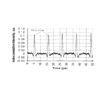
FIG. 7 is an autocorrelation plot of a pulse train obtained at 60 mA with a
measured
period of 10.81ps;
FIG. 8 shows two comparative autocorrelation traces showing the effect of
excluding
the C-band peak demonstrating that interband mode locking is produced; and
FIGs. 9a-c show how to achieve multi-band mode locking using the active medium
of
the previous examples, using a coating to selectively attenuate modes within
the cavity.
CA 02674959 2009-06-25
Description of Preferred Embodiments
[0021]
Mode locked laser diodes are provided herein, as are methods of producing a
mode locked multi-band multiwavelength laser output. In accordance with the
invention,
multi-bard multiwavelength laser diodes are provided in the form of a pin
diode with a
quantum dot (QD) active medium wherein a dynamic dispersion that varies with
operating
conditions of the laser is controlled to correct a fixed dispersion of the
laser, at least across
two wavelength regions where the cavity loss function is majorized by gain
curve of the laser.
This results in (intraband) mode locking of the channels within each of the
wavelength
regions.
PIN diode structure
[0022]
More specifically, in accordance with the invention, a laser diode is provided
that
includes an active medium that includes at least one layer of QDs embedded in
an optical
waveguide, so that the QDs are spatially isolated from one another in 3
dimensions. The
active medium is enclosed by a cavity interface, which includes a facet for
selectively
transmitting laser output and reflecting light back into the cavity.
[0023] In
general, the more QD layers, and the higher the QD density of the layers, the
more optical power is produced by a given pump current as there are
effectively more
emitters. At the same time it is increasingly difficult to produce higher and
higher stacks of
QD layers using the presently preferred methods, such as epitaxial growth and
self-
assembly. Accordingly a preferable number of layers of QDs is at least two
layers or three
layers. With current methods less than 30, or 15 layers, more preferably less
than 12 or 10
layers are generally preferable. Specifically 5 layers are shown to work well.
[0024] The
optical waveguide and QDs are formed of semiconductors. The selection of
fabrication methods (chemical vapour deposition, chemical beam epitaxy, etc.)
and
compounds are known and it is within the scope of the person of ordinary skill
in the art to do
so.
Chemical beam epitaxy is preferred because it provides for integration with
semiconductors in a straightforward manner. In the illustrated embodiments,
the wetting
layers are InGaAsP, the QD layers are formed of InAs layers, and the active
medium/waveguide is clad in InP. While the QDs used in the verification of the
invention are
formed of InAs, it will be appreciated that other QDs such as GaAs, InGaAs,
CdSe, and GaN
could be used alternatively.
[0025] The
QDs have a distribution of sizes and geometries, such as provided by self-
assembly to provide inhomogeneous gain broadening. The QDs used in the
demonstration of
6
CA 02674959 2009-06-25
the invention were produced by depositing a continuous layer using chemical
beam epitaxy,
followed by strain release to crack the layer to form the QDs by self
assembly, and then a
resurfacing of the cracked layer, in a manner that is known in the art, The
QDs were
substantially planar sheets having dimensions in the neighbourhood of 10-8 m
in two
dimensions and a few nanometers in the third. It will be appreciated that QD
layers having
various distributions of sizes, geometries, and compositions are known by
changing growth
parameters, strains and thermal treatments, as well as by controlling a
crystal lattice
mismatch between the deposited layer and substrate.
[0026] Generally a high QD density is desirable. Applicant has found QD
layer densities
on the order of 1010 per cm2 to be more than adequate, although different
densities may be
used. Lower QD densities may be possible if operation above the splitting
threshold of the
AC Stark effect is not used to achieve the multiple bands.
[0027] As is well known in the art, such layers of QDs produce an
inhomogeneously
broadened gain curve. Furthermore it is known that modification of the growth
parameters
(strains, substrate surface properties, thermal treatments, thicknesses,
compositions,
deposition rates, etc.) have known effects on the gain curves of the produced
layers.
[0028] Only modes of wavelengths that have higher gain than cavity loss
will lase. As
cavity losses are typically functions of wavelength, it is useful to
selectively attenuate (absorb
or otherwise remove from the cavity) wavelength modes of the compound ASE
spectrum
different from those that are to lase. By attenuation of the wavelengths that
are not desired
for lasing, the QDs that would otherwise have been absorbed at these
wavelengths become
available for the lasing of the desired modes. This can be performed using a
controllable
variable optical attenuator, or an absorber, for example, and can be effected
by controlling
cavity interfaces, such as a pair of facets defining the longitudinal mode
length of the cavity.
[0029] One important effect of such attenuation is that the design of the
laser is not
limited to a peak of the gain curve of the QD layer. By selective frequency
attenuation in the
neighbourhood of the peak at cavity interfaces, a different, adjacent
wavelength region
becomes the effective local peak. This permits the selection of A, a
difference between
peak center frequencies of the laser output and gain curves.
[0030] Between the QD layers, waveguide layers are deposited. These layers
are
generally thicker and provide a support for the application of successive QD
layers. The
waveguide layers are important because they typically contribute significant
dispersion as
well as some absorption to the cavity.
7
CA 02674959 2009-06-25
[0031] On
opposite large faces of the active medium/waveguide are means for
conducting electrical current through the active medium. Oppositely doped
semiconductor
cladding coupled to junctions can be used. The junctions with the cladding
preferably serve
as cavity interfaces. Pump electricity is provided through these junctions to
pump the QDs.
[0032]
While the cladding provides cavity interfaces on two sides, it will be
appreciated
by those skilled in the art that other cavity interfaces are chosen to enhance
desired (e.g.
usually longitudinal) modes within the cavity, and to suppress others.
[0033] In
the following examples, the configurations of the PIN diode lasers are assumed
to be ridge-type waveguides. It will be appreciated that other configurations
are possible,
such as quadrupolar designs, and any other geometric layout can alternatively
be used.
[0034] The
operational current of the laser is chosen simultaneously to supply enough
pump energy so that the gain curve exceeds cavity loss over two or more
(lasing) wavelength
regions (lasing bands), and to produce a dynamic dispersion that results in a
substantially
constant dispersion within at least two lasing bands.
Multi-band lasing methods
Multiple gain curves
[0035] As
the active medium may contain a number of layers of QDs, and as different
kinds of QDs are known to exhibit different gain curves, one way that multiple
bands can be
achieved is to use two (or more) kinds of layers, where the different kinds of
layers are
produced using different protocols to achieve different peak gains. By
including multiple
layers of the QDs of different kinds, multiple bands above the lasing
threshold can be
achieved. Cavities containing these layers exhibit compound ASE spectra with
peaks at
multiple wavelengths. It is this compound ASE spectrum that starts the lasing
process of the
material. Selection of the layers therefore permits the selection of different
wavelength
regions of the peaks.
[0036] A
compound gain curve can be chosen by multiplexing of QD of various sizes and
geometries. If the active medium includes N, layers of QDs, for i=1,
m<15, the compound
gain curve of the active medium would be the linear superposition of the m
gain curves. If
each layer of QDs and has a gain curve with a respective lasing band, m-band
multiwavelength lasers would be produced. For example, a dual band ASE
spectrum was
reported in [34] using two different-sized QD families, and 5 multi-band ASE
spectra of QD
layers having different heights resulting in shifted bands were published by
Applicant in [35].
8
CA 02674959 2015-11-04
The contents of [34] and [35] are familiar to one skilled in the art. FIG. 1
reproduces an
image from this reference showing that it is possible to produce multi-band
multiwavelength
photoluminescent stacked QD structures. The foregoing 2 examples are not
exhaustive of
the variety of possible combinations of QD layers that can be assembled to
form active
media.
[0037] Synthesizing and/or stitching the gain curves of each band with the
proved
technologies in [34-35], produces compound gain curves having a variety of
shapes,
including multi-peaked gain curves having desired amplitudes. Generally peaks
that result in
output spectra with equal amplitudes are desired. Accordingly, desired band
peak amplitudes
could be chosen to compensate for frequency variance of cavity loss.
Furthermore, as the higher frequency bands in the frequency domain may re-pump
the lower
frequency bands, leading to the quenching of the higher frequency bands in
use, a further
reduction in the lower frequency bands and increase in higher frequency bands
may be
called for. By selecting the layer numbers N1 and the ASE spectra for all
layers, a gain curve
with multiple and equal bands as shown in FIG. 2 can be created.
[0038] While the combinations of QD layers are preferably stacked to minimize
a number of
electrodes, it will be appreciated that other arrangements are possible,
including side-by-side
arrangements, where optical waveguide continuity is provided for.
Attenuation
[0039] Inversely, it is possible to attenuate a broad ASE spectrum at select
frequencies to
produce a compound ASE spectrum having multiple peaks at desired wavelength
regions
using known thin film techniques. For example, it is possible to attenuate by
incorporating
absorbers, or elements that simply corrupt the coherence (in space and/or
time) of select
wavelengths, or in other ways known in the art, but in accordance with a
preferred
embodiment, cavity interfaces are used to selectively transmit modes that are
at frequencies
distant the desired bands.
[0040] ASE spectra are affected by selecting cavity interfaces. If we take the
cavity to have a
rectangular ridge-waveguide configuration having two opposing facets at
smallest faces,
cladding along largest, opposing, faces, and along longitudinal high aspect
ratio faces, a
naked cavity interface boundary, selection of the longitudinal modes is
provided with high
reflectivity coatings at the facets (for near normal incidence) in comparison
with high
transmission along the longitudinal high aspect ratio faces. Along transverse
directions of the
cavity, for a typical rectangular cavity, modes are attenuated. Assuming this
layout, for
9
CA 02674959 2015-11-04
example, coatings serve as reflectors at respective facets, one of which, is
an output
coupler of the laser.
[0041] For example, given an active medium with QD layers embedded in a
semiconductor
waveguide that exhibits a very broad gain curve, such as shown in FIG. 9a
(described below
in relation to Example 2) or in Ref. [1] the contents of which being familiar
to one skilled in
the art, it is well known in the art to select a coating for a cavity mirror
or mirrors, for which
one or more central bands have lower reflectivity while the side bands have
higher
reflectivity.
[0042] The quantitative design of band reflectivity is preferably based on ASE
measurements made before coatings are added, using the cavity loss function,
and cavity
length, as well as the center wavelengths and shapes of the desired lasing
bands.
AC Stark splitting
[0043] According to the current understanding of lasers, lasing modes
generated by
electrically pumped QDs (ASE) interact again with QDs themselves inside the
same cavity.
The strengths of the looped interactions between QDs and self-generated lasing
modes are
represented by Rabi frequencies [21]. These interactions lead to spectral
changes in the
laser output from the gain curve and ASE spectra. For a given cavity that
selects some
interactions, for strong enough electrical pumping, energy level splittings of
the QD
ensemble would be expected to occur by amounts given by the Rabi frequencies;
this
phenomenon is referred to as AC Stark splitting.
[0044] FIG. 3 is a plot showing a theoretical calculation of laser energy
output (log10(02))
v.s. A at different pumping levels P/Pth. As previously stated A is the detune
frequency i.e.
the difference between the peak of a QD gain curve and the resulting lasing
frequency. 2
is a quantity proportional to lasing intensity. P is the electrical pump
intensity (current), and
Pth is the pump intensity at the lasing threshold, respectively. This graph
illustrates the AC
Stark splitting. Resulting lasing spectra are dramatically modified by the AC
Stark effect. For
example, one-band lasing would be transferred into two-band lasing.
[0045] It should be noted that P is the only condition that is controlled
dynamically, although
by varying reflectance at the output coupler, 02 can, in principle, be
independently modified.
As previously stated, A can be modified by frequency selective attenuation,
but is generally
a fixed property of the PIN diode laser, as is Pth.
CA 02674959 2009-06-25
[0046] Our
theoretical results graphed in FIG. 3 show that lasing occurs initially within
a
band centered at A = 0 and the number of lasing modes is determined by the
bandwidth and
the intracavity gain and loss over this band. As P/Pth increases, intracavity
lasing intensity
becomes so strong that two-band lasing spectra are generated at a given
threshold.
[0047]
Accordingly three methods are proposed to produce multi-band multiwavelength
PIN diode lasers. It will be appreciated that each combination of the above
methods is
contemplated by the Applicant.
Mode locking
[0048]
Dispersion within the cavity occurs when different modes propagate at
different
velocities. If the modes propagate at different velocities through a same
distance, the laser
output is a continuous wave. Mode locking across a multiwavelength band is
achieved when
the standing waves generated by the modes are of a substantially constant
phase difference
at an output coupler of the laser, where the modes interfere to produce output
that is
temporally pulsed, even if the pumping is continuous. If
the modes have different
propagation rates, the relative phases vary continuously, and there is no mode
locking.
[0049]
Along with the constraints on the waveguide material, and cavity design to
provide
low cavity losses, it is also desired to provide a fixed dispersion that is
substantially constant,
at least over desired lasing wavelength regions. The fixed dispersion is
typically the sum of
the waveguide dispersion, material dispersion, and mirror dispersions, though
in principle any
number of elements can be provided within the cavity to induce a change in
dispersion. It is
well known in the art how to perform chromatic dispersion compensation. A
constant
dispersion is desired to produce uniform mode spacings (Av), i.e. the
frequency differences
between the modes (the multiple wavelengths) within a band. Note that the mode
spacing is
given by Av = c 1[2Lng(v)] where L is the cavity length, c is the speed of
light, and ng(v) is
the group index of refraction of the cavity.
[0050]
Herein "substantially constant" means that the variations in phase between
pairs
of the modes produces a chirping of the resulting pulse so that it is less
than 1/2 the interval
between the pulses. Mathematically, this means:
[0051] The
static dispersion due to materials, waveguides and mirror coatings are not the
only factors affecting cavity index ng(v), and its variation over lasing
bands. Dynamic
dispersion terms relating to the interaction of QD excitons with intracavity
laser fields can
significantly impact the variations of the index of refraction as a function
of frequency over the
11
CA 02674959 2009-06-25
lasing bands. Where total dispersion within a band is minimized, four-wave
mixing (FWM) is
dramatically enhanced. If lasing bands are broad enough, several or tens or
hundreds of
cavity modes would lase and their phases would be locked through FVVM and
other nonlinear
processes. These phase-locked lasing modes lead initially to random intensity
spikes in the
time domain, and subsequently to periodic pulse train due to self-lensing
caused by the
optical Kerr effect, as the waveguides serve as thick hard apertures, and any
injection current
variation and/or temperature instability serves as a mode-locking starter.
[0052]
Firstly, the group phase change of the intracavity laser field amplitude
induced by
the interaction between QDs and self-generated intercavity lasing modes could
be formulated
as = arctan 7A /[42 + S-22 ¨
¨1)271} under some proper approximations, where
Pth Pth
ca, is the dipole moment decay rate.
[0053] The
dynamic group phase change represents a phase shift per unit time as a
function of frequency. The differences between phase shifts as a function of
frequency and
is a comparative measure. This quantity is directly related to the dynamic
dispersion. By
adjusting the operation parameters such as the pump factor P/Pth and the
effective Rabi
frequency VA.2 + SY" , the group phase change v(A) could be positive or
negative in some
specific detuning A areas.
[0054]
FIG. 4 is a graph showing group phase change over the cavity for a range of
frequencies (-4< A <4) for two different pump factors: P/P(h=1.01, 2. In the
graph of FIG. 4,
the dipole moment decay rate is taken to be a unitary constant. This is not an
accurate
value, and in practice it is difficult to determine this value, given that the
decay rate is too fast
to be captured on commonly available detection equipment. As given in the
group phase
change formula above, when A' + C)2 Pth
-1)702h V(A) 0 only if A 0. Thus for
P/Pth=1.01 as shown in FIG. 4, the group phase change is negative for A <0,
positive for A
>0, and 0 only at A = 0. In contrast, when A2 +Q2 5- (Pi Pth ¨1)7a2n (e.g.
P/Pth=2) v(A) is
negative from A = 0..1.2 and A <-1.2. This means that the AC Stark splitting
results in two
areas almost symmetric about A with substantially equal negative dispersion.
This permits
bands formed near these peaks to compensate a static (positive) dispersion
caused by
waveguides and coatings so that the total intracavity dispersion is close to
zero over these
two areas. Furthermore, as the P/Pth=2 curve shows minima near A = 1.2 there
is a
neighbourhood around these points in which a difference between a relatively
constant, fixed
dispersion will be equally compensated at two points. These two neighbourhoods
are nearly
12
CA 02674959 2009-06-25
symmetric about A = 0 axis. Remarkably, there is overlap between both the two
neighbourhoods and the two bands illustrated in FIG. 3, and thus two-color
mode-locking
lasers could be generated from the AC Stark splitting. More remarkable is that
over a
substantial range of separations of the bands, (i.e. for a range of P/Pth) the
overlap between
the neighbourhood and the bands is maintained. So not only does peak division
by AC Stark
splitting result in, for a judicious selection of cavity parameters, dual band
mode locking; but it
also provides for variable separation (tunable) dual band mode locking.
[0055] It should further be noted that a desired dispersion once computed
having regard
to the material and waveguide dispersions, and/or the coating dispersions by
intracavity
dispersion compensation. Alternatively or additionally, the coating can be
chosen with the
additional constraint to provide a desired fixed cavity dispersion.
[0056] It will be appreciated by those of skill in the art that a
relatively high current may
be required in order to produce AC Stark splitting, and that there are several
drawbacks to
operation at high current pumping levels, including the requirement for
thermal control over
the PIN diode laser. It is also possible to use the dynamic dispersion at
lower pump powers
to produce a similar effect. For example, at P/Pth = 1.01, a group phase
distribution as
shown in FIG. 4 is produced. By choosing design electives to produce a cavity
fixed
dispersion that produces substantially equal phases across various frequency
regions, and
possibly a substantially equal dispersion over two or more frequency regions,
intraband
mode locking and interband mode locking can be achieved, respectively. It may
also be
possible to provide a fixed dispersion that provides for dispersion
compensation at different
bands at different operational conditions, such as for different P/Pth values.
[0057] Furthermore, the use of attenuation and/or multilayer designs to
derive compound
(multi-band) gain curves, can also be subject to AC Stark splitting. If the
(compound) gain
curve has sufficient amplitude, and the active media can support elevated pump
currents,
2N-bands of could be realized as the AC Stark effect could result in two areas
around each
of N peaks of the gain curves with the required dispersion to compensate for
the fixed cavity
dispersion within each band.
[0058] The foregoing theory is believed to correctly describe the AC Stark
effect and its
operation in the present invention, and is included as an explanation of the
experimental
results below, which support the foregoing theory, however the theory is not
intended to be
limiting.
13
CA 02674959 2009-06-25
Experiment 1: AC Stark splitting
Laser diode specification
[0059]
FIG. 5 shows two SEM images of an active medium used to produce a laser
diode, and a schematic illustration of such a diode, according to an
embodiment of the
invention. The rightmost image is a high magnification SEM image of a cross-
section of the
active medium showing 5 stacked QD layers. The leftmost image is at a lower
magnification
and shows the ridge waveguide structure in cross-section. An InAs/InGaAsP
active medium
with a self-assembled QD was grown by chemical beam epitaxy (CBE) on exactly
oriented
(100) InP n-type substrates, in a manner known in the art. The undoped active
regions
consisted of five stacked layers of self-assembled InAs QDs embedded in
quaternary
!no 816Ga0.392ASO 392P0 608 (1.15Q), providing three-dimensional electron
confinement.
[0060] The
QDs were formed by cracking substantially planar sheets having dimensions
in the neighbourhood of 10-8 m in two dimensions on average, followed by
resurfacing of the
produced quantum dots so that they all have heights of a few nanometers in the
third,
[0061]
From transmission electron microscopy (TEM) measurements, the QD density in
each QD layer was computed. The approximate QD density was found to be 3-5x101
per
CM2 .
[0062]
Optical confinement in the growth direction was achieved with a planar
waveguide
layered in between QD layers in the vertical direction to produce an active
medium.
In0.816Ga0.392AS0.392P0.608 layers of 10 nm height in between the QD layers,
and a thicker layer
of the In 816Ga0.392ASO 392P0 608 was deposited above and below.
[0063] The
active medium was clad in an n-type doped InP bottom layer and a p-type
doped InP top layer. The top cladding was covered with a cap of p+-
1110.522Ga0478As to ensure
good ohmic contact to the top metal stack. The active medium itself served as
the optical
pumping/lasing medium, a filter for longitudinal modes, a polarization
maintaining
component, and cavity mirrors as well.
Accordingly it will be appreciated that changing
properties of the QD layers, and/or the waveguide layers in which the QDs are
embedded,
will largely change the properties of the laser diode.
[0064] The
multi-band multiwavelength mode-locking lasers produced has a ridge-
waveguide Fabry-Perot (F-P) cavity structure, which was cleaved
perpendicularly to the
diode junction plane, at a length of L = 456 pm. The area of the active medium
is 1,824 pm2.
14
CA 02674959 2015-11-04
[0065] FIG. 6b is the measured ASE spectrum of the specific cavity cut to this
size, before the
addition of the output coupler. This curve shows a very broad, high power ASE
response. Cavities with comparable ASE spectra are particularly well suited to
the invention.
The optical absorption in the frequency range of delta 5 to -5 is relatively
constant, varying from 8-
20db/cm. The effective index of refraction in this neighbourhood is about 3.4-
3.6. A
static dispersion of this cavity (prior to facet coating) is deduced (from
details reported in [38]
the contents of which are familiar to one skilled in the art) to be about -
5.1*10^(-4)/nm, which means
that when wavelength increases 1 nm, the group refractive index decreases
0.00051.
[0066] Subsequently, one of the laser end facets was coated to produce 95%
reflection for
wavelengths within 1500 nm - 1600 nm, and the other served as the output
coupler, having about
30% reflectance. The both facets had flat spectral response in the wavelength
region of lasing. The
claddings of doped InP provide desired cavity interfaces that effectively
select longitudinal modes
within the cavity.
Measurement apparatus
[0067] The laser output at one facet of the laser diode was coupled by a fiber
with a numerical
aperture of 0.35 and mode field diameter 4pm, and sent to an optical spectrum
analyzer (OSA) and a
power meter (PM) through a SMF-28 fiber spliced with that fiber. The laser
sample was mounted on
a thermoelectric cooler (TEC) at room temperature, and driven by continuous
pump currents. Various
temperatures were experimented with and it was found that an optimal
temperature, for a narrowest
pulse duration, was about 18 C.
Laser output
=
[0068] FIGs. 6a shows 6 plots of experimental lasing emission spectra taken
under pump currents
of 30 mA, 35 mA, 40 mA, 50 mA, 60mA, and 70mA, as labeled. Pth is about 17.2
mA. The pump
voltage varied within about 2-4.5 volts. At each of these pump factors, a mode-
locked spectral output
of a single band, or dual band laser is produced. It is an advantage of the
present invention that the
same laser can be used for producing a single band that is mode locked, or
multiple bands.
[0069] As the current increases, the output spectrum broadens. Two distinct
bands can be resolved
at a current of 40mA and above. The higher the current applied across the
active medium, the larger
the wavelength separation between the two splitting bands caused by the AC
Stark effect. In all
cases the dual bands are intraband as well as interband mode locked.
CA 02674959 2009-06-25
[0070] At a pump current of 35 mA, a 11 channels having mode spacings of
745.2 pm
was observed. The band was centered on 1554.3 nm, and had a bandwidth of
(FWHM) 8.2
nm.
[0071] In contrast, at 60 mA, the laser had 15 modes, of which 10 modes
were in a band
from 1568nm to 1576nm (within the L-band), and 5 modes were in a distinct band
from
1542nm to 1546nm (within the C-band). The 10 L-band modes had a slightly
greater mode
spacing at 763.0 pm, and the 5 C-band modes had a 732.4 pm mode spacing. The
separation between two band center peaks at 60mA was 28.0 nm, corresponding to
a
frequency difference of 3.462 THz, and the two bands were located almost
symmetrically
around 1557.7nm, which coincides with the central lasing wavelength at a bias
current of 30
mA.
[0072] The fact that the same laser can be made to produce a single band or
pairs of
bands of different separations by simply applying different currents is of
considerable value.
[0073] Naturally every separation up to 28 nm can be achieved with a
corresponding
current between 30 and 60 mA, and greater separations (such as the 35 nm
separation
shown at 70 mA) are possible.
Mode locking
[0074] To assess the temporal properties of the laser output, the above-
identified diode
laser setup (specifically the SMF-28 fiber) was coupled to a fiber-based
background free 2nd
Harmonic generation autocorrelator made by Femtochrome Research Inc. (FR-
103HS).
[0075] FIG. 7 shows the emitted pulse train at a drive current of 60 mA
from which the
repetition rate was measured to be 92.5 1.25 GHz. It will be appreciated that
the high
regularity of the autocorrelated amplitude over time is a strong indicator
that the laser is
mode locked.
[0076] Furthermore, to confirm the interband mode-locking for both the C-
and L-bands,
the C-band modes were filtered using a homemade thin film bandpass filter.
[0077] In FIG. 8 (right panel) shows the autocorrelation intensity plot of
the L-band alone
(left panel). As this pulse exhibited the same repetition rate as the joint L-
and C-band
pulses, it is clear that interband mode locking was achieved. The pulse
durations for the
single L-band peak centered at Al and the dual bands at Al and /1,,, , were
657fs and 955fs,
respectively, assuming Gaussian temporal pulse profiles. From the self-
correlation data and
16
CA 02674959 2009-06-25
the cross-correlation data collected, the relative time jitter between the two-
band pulse
sequences was too small to be measured with the 10fs-resolution autocorrelator
used. The
45% increase in temporal bandwidth is explained by bandwidth differences in
the two bands.
Example 2 (prophetic): Attenuation
[0078] FIGs. 9a-c are graphs showing how attenuation at facets can be used
to generate
multi-band multiwavelength lasing. FIG. 9a is a graph of the obtained ASE
spectrum of the
cavity produced in relation to example 1, prior to addition of a facet. The
multiwavelength
channel structure is not presented as the resolution of the OSA was lower than
the mode
spacing. Only the band structure is manifest.
[0079] It is noted in FIG. 9a that the breadth of the uncoated ASE spectrum
is great, with
a FWHM of 170nm. It is known in the art to provide cavity interfaces that
selectively transmit
modes as a function of frequency. Shown in FIG. 9b is a desired relative
reflection spectrum
designed to effectively remove modes having wavelengths of 1510-1535 nm and
1565-1585
nm from the cavity, as well as to reduce the amplitude of a center peak near
1550 nm to
somewhat flatten the peak of the uncoated ASE spectrum. It is known in the art
how to
produce coatings to this specification.
[0080] The band structure of a resulting ASE spectrum expected for a cavity
having
facets exhibiting a relative reflection spectrum according to FIG. 9b is shown
in FIG. 9c.
Once again the multiwavelength channel structure is not illustrated, just the
band structure.
Given the fact that the attenuation cavity losses (losses due to material and
waveguide + the
losses at the interface) over the bands near 1490, 1550, and 1610 are
majorized by the ASE
of FIG. 9b, there will be lasing in each of these bands.
[0081] By analogy with the single band multiwavelength mode locked lasing
demonstrated with the example above, this resulting ASE spectrum is expected
to exhibit
interband mode-locking.
[0082] Other advantages that are inherent to the structure are obvious to
one skilled in
the art. The embodiments are described herein illustratively and are not meant
to limit the
scope of the invention as claimed. Variations of the foregoing embodiments
will be evident to
a person of ordinary skill and are intended by the inventor to be encompassed
by the
following claims.
17
CA 02674959 2009-06-25
[0083] References:
1. Z. G. Lu et al. "Ultra-broadband quantum-dot semiconductor amplifier and
its
applications" In Proc. of Opt. Fiber Comm. (OFC'2007), JThA33, Anaheim, CA,
USA, March
2007.
2. J. Liu et al. "Uniform 90-channel multiwavelength InAs/InGaAsP quantum dot
laser"
Electron. Lett., 43, 458-460 (2007).
3. J. Liu et al. "1.6-pm multiwavelength emission of an InAs/InGaAsP
quantum dot laser"
IEEE Photonics Technol. Lett., 20, 81-83 (2008).
4. A. Kovsh et al. "Quantum dot laser with 75 nm broad spectrum of
emission" Opt. Lett.,
32, 793-795 (2007).
5. Q. Mao et al. "Multiwavelength erbium-doped fiber lasers with active
overlapping linear
cavities" J. Lightwave Technol., vol.21, pp.160-169, January 2003.
6. X. P. Dong et al. "Multiwavelength erbium-doped fiber laser based on a high
birefringence
fiber loop mirror" Electron. Lett., vol.36, pp. 1609-1610, 2000.
7. J. Sun et al. "Multiwavelength erbium-doped fiber lasers exploiting
polarization hole
burning" Optic. Communications, vol.182, pp. 193-197, 2000.
8. S. Pradhan et al. "Multiwavelength distributed Bragg reflector fiber
laser" Electronics
Letters, vol.42, (17), pp.963-964, 2006.
9. G. Das et al. "L-band multiwavelength fiber laser using an elliptical
fiber" IEEE Photon.
Technol. Lett., vol.14, pp.606-608, May 2002.
10. Y. G. Han et al. "Multiwavelength Raman fiber-ring laser based on tunable
cascaded
long-period fiber gratings" IEEE Photon. Technol. Lett., vol.15, pp.383-385,
March 2003.
11. J. Yang et al. "Multiwavelength tunable fiber ring laser based on sampled
chirp fiber
Bragg grating" IEEE Photon. Technol. Lett., vol.16, pp.1026-1028, April 2004.
12. P. C. Peng et al. "A tunable dual-wavelength erbium-doped fiber ring laser
using a self-
seeded Fabry-Perot laser diode" IEEE Photon. Technol. Lett., vol.15, pp.661-
663, May 2003.
18
CA 02674959 2009-06-25
13. Z. G. Lu et al. "High-power multiwavelength Er3+-Y133+ codoped double-
cladding fiber ring
laser" IEEE Photon., Technol. Lett., vol.17, (9), pp.1821-1823, 2005.
14. Z. G. Lu et al. "A widely tunable narrow-linewidth triple-wavelength
erbium-doped fiber
ring laser" IEEE Photon. Technol. Lett., vol.17, (1), pp.22-24, 2005.
15. H. Chen "Multiwavelength fiber ring lasing by use of a semiconductor
optical amplifier"
Opt. Lett., vol.30, pp. 619-621, 2005.
16. Z. G. Lu et al. "Frequency comb generation by cascade cavity-enhanced four-
wave
mixing in a semiconductor optical amplifier" Microwave and Optical Technology
Letters, 23,
3, pp. 134-137, 1999.
17. M. T. Hill et al. "Integrated two-state AWG-based multiwavelength laser"
IEEE Photonics
Technol. Lett., vol.17, pp. 956-958, 2005.
18. X. Dong et al. "Multiwavelength Raman laser with a continuously- tunable
spacing"
Optics Express, vol.8, pp. 3288-3293, 2006.
19, Z. Lu et at. "Quantum-dot-based semiconductor waveguide devices" US Patent
Application 11983-1, Invention disclosure (October 2007).
20. S. Arahira et at. "160-gb/s OTDM signal source with 3R function utilizing
ultrafast mode-
locked laser diodes and modified NOLM" IEEE Photonics Technol. Lett., 17, 992-
994 (2005).
21. H. Htoon et at. "Interplay of Rabi oscillations and quantum interference
in semiconductor
quantum dots" Phys. Rev. Lett., 88, 087401 (2002).
22. M. R. X. de Barros et al. "Two-color synchronousely mode-locked
femtosecond Ti:
sapphire laser" Opt. Lett., 18, 831-833 (1993).
23. J. Liu et al. "Fabrication and stitching of embedded multi-layer micro-
gratings in fused
silica glass by fs laser pulses" Applied Physics B: Lasers and Optics, vol.86,
No.1, 151-154
(2007).
24. C. Gosset et al. "Subpicosecond pulse generation at 134GHz and low
radiofrequency
spectral linewidth in quantum dash-based Fabry-Perot lasers emittings at
1.5,um" Electron.
Lett., 42, 91-92 (2006).
19
CA 02674959 2009-06-25
25. X. Huang et al. "Passive mode-locking in 1.3 mm two-section InAs quantum
dot lasers"
Appl. Phys. Lett., 78, 2825-2827 (2001).
26. M. Kuntz et al. "35 GHz mode-locking of 1.3 mm quantum dot lasers" App!.
Phys. Lett.,
85, 843-845 (2004).
27. J. M. Evans et al. "Dual-wavelength self-mode-locked Ti: sapphire laser"
Opt. Lett., 13,
1074-1076, (1993).
28. F. C. Turner et al. "Anti-Stokes enhancement of multifrequency Raman
generation in a
hollow fiber" Opt. Lett., 33, 405-407 (2008).
29. M. Katsuragawa et al. "Generation of a 10.6-THz ultrahigh-repetition-rate
train by
synthesizing phase-coherent Raman sidebands" Optics Express, 13, 5628-5634
(2005).
30. G. Park et al. "Low-threshold oxide-confined 1.3-pm quantum dot laser"
IEEE Photonics
Technol. Lett., vol.13, pp. 230-232, 2000.
31. H. Saito et al. "Low chirp observed in directly modulated quantum dot
lasers" IEEE
Photonics Technol. Lett. vol.12, pp. 1298-1300, 2000.
32. G. Ortner et al. "External cavity InAs/InP quantum dot laser with a tuning
range of
166nm" Applied Phys. Lett., vol.88, pp. 121119, 2006.
33. X. Huang et al. "Passive mode-locking in 1.3-pm two-section InAs quantum
lasers"
Applied Phys. Lett., vol.19, pp. 2825-2827, 2001.
34. Y. I. Mazur et al. "Tailoring of high-temperature photoluminescence in
InAs/GaAs bilayer
quantum dot structures" Journal of Applied Physics, vol.98, 053515 (2005).
35. P. J. Poole et al. "Using As/P exchange processes to modify InAs/InP
quantum dots"
Journal of Crystal Growth, vol.257, 89-96(2003).
36. F. X. Kartner et al. "Design and fabrication of double-chirped mirrors"
Opt. Letts., vol.22,
No.11, 831-833(1997).
37. J. A. Dobrowolski et al. "Refinement of optical multilayer systems with
different
optimization procedures" App!. Optics, vol.29, No.19, 2876-2893 (1990).
38. J. Liu, et al, "1.6-pm multiwavelength emission of an InAs/InGaAsP quantum
dot laser,"
IEEE Photonics Technol. Lett., 20. 81-83 (2008).