Note: Descriptions are shown in the official language in which they were submitted.
CA 02675382 2009-07-13
WO 2008/094271 PCT/US2007/066358
CHOPPER-STABILIZED INSTRUMENTATION AMPLIFIER
TECHNICAL FIELD
The invention relates to amplifiers and, more particularly, to instrumentation
amplifiers for accurate signal measurement.
BACKGROUND
Instrumentation amplifiers are used to accurately measure a variety of test
and
measurement signals. A medical instrumentation amplifier, for example, may be
configured
to measure physiological signals, such as electrocardiogram (ECG),
electromyogram (EMG),
electroencephalogram (EEG), pressure, impedance, and motion signals.
Typically,
instrumentation amplifiers are constructed as differential amplifiers
exhibiting low offset,
low drift, low noise, high common mode rejection, high loop gain, and high
input impedance.
In many cases, instrumentation amplifiers may require careful matching and
trimming of
circuit components to achieve a high degree of accuracy.
An instrumentation amplifier may be constructed with a discrete time switched
capacitor architecture that obtains discrete signal samples. However, a
discrete time
architecture can produce undesirable aliasing of noise and signals,
undermining the accuracy
of measurement signals. Alternatively, an instrumentation amplifier may employ
a chopper
stabilized architecture in which a chopper circuit up-modulates a measurement
signal into a
higher frequency band to remove noise and offset. A chopper-stabilized
architecture may
have a limited bandwidth, however, producing a large ripple in the passband.
The ripple may
make implementation of chopper-stabilized designs difficult in low power
applications.
SUMMARY
This disclosure describes a chopper stabilized instrumentation amplifier. The
instrumentation amplifier is configured to achieve stable measurements at low
frequency
with very low power. The instrumentation amplifier uses a differential
architecture and a
mixer amplifier to substantially eliminate noise and offset from an output
signal produced by
the amplifier. Dynamic limitations, i.e., glitching, that result from chopper
stabilization at
low power are substantially eliminated or reduced through a combination of
chopping at low
CA 02675382 2009-07-13
WO 2008/094271 PCT/US2007/066358
impedance nodes within the mixer amplifier and feedback. The signal path of
the
instrumentation amplifier operates as a continuous time system, providing
minimal aliasing
of noise or external signals entering the signal pathway at the chop frequency
or its
harmonics. In this manner, the instrumentation amplifier can be used in a low
power system,
such as an implantable medical device, to provide a stable, low-noise output
signal.
In one embodiment, the invention provides a chopper-stabilized instrumentation
amplifier comprising a first modulator that modulates an amplitude of a
differential input
signal at a clock frequency to produce a modulated signal, a mixer amplifier
that amplifies
the modulated signal to produce an amplified signal and demodulates the
amplified signal at
the clock frequency to produce an output signal, a second modulator that
modulates an
amplitude of the output signal at the clock frequency, and a feedback path
that applies the
modulated output signal as a differential feedback signal to the modulated
input signal.
In another embodiment, the invention provides a physiological sensing device
comprising a physiological sensor that generates a differential input signal
indicative of a
physiological condition, and a chopper-stabilized instrumentation amplifier
comprising a first
modulator that modulates an amplitude of the differential input signal at a
clock frequency to
produce a modulated signal, a mixer amplifier that amplifies the modulated
signal to produce
an amplified signal and demodulates the amplified signal at the clock
frequency to produce
an output signal, a second modulator that modulates an amplitude of the output
signal at the
clock frequency, and a feedback path that applies the modulated output signal
as a
differential feedback signal to the modulated input signal.
In an additional embodiment, the invention provides a method comprising
modulating
an amplitude of a differential input signal at a clock frequency to produce a
modulated signal,
amplifying the modulated signal in a mixer amplifier to produce an amplified
signal,
demodulating the amplified signal in the mixer amplifier at the clock
frequency to produce an
output signal, modulating an amplitude of the output signal at the clock
frequency, applying
the modulated output signal as a differential feedback signal to the modulated
input signal via
a first feedback path.
The details of one or more embodiments of the invention are set forth in the
accompanying drawings and the description below. Other features, objects, and
advantages
of the invention will be apparent from the description and drawings, and from
the claims.
2
CA 02675382 2009-07-13
WO 2008/094271 PCT/US2007/066358
BRIEF DESCRIPTION OF DRAWINGS
FIG. 1 is a block diagram illustrating a chopper-stabilized instrumentation
amplifier
configured to achieve stable measurement at low frequency with very low power.
FIG. 2 is a diagram illustrating a signal flow path of the instrumentation
amplifier of
FIG. 1.
FIGS. 3A-D are graphs illustrating frequency components of a signal at various
stages within the signal flow path of FIG. 2.
FIGS. 4A-D are graphs illustrating a signal at different stages within the
signal flow
lo path of FIG. 2.
FIG. 5 is graph illustrating exemplary noise performance of a chopper-
stabilized
instrumentation amplifier.
FIG. 6 is a circuit diagram illustrating a chopper-stabilized mixer amplifier
forming
part of an instrumentation amplifier.
FIG. 7 is a block diagram illustrating an example embodiment of the
instrumentation
amplifier of FIG. 1 in greater detail.
FIG. 8 is a circuit diagram illustrating an example embodiment of the
instrumentation
amplifier of FIG. 1 for measurement of voltage signals.
FIG. 9 is a circuit diagram illustrating another example embodiment of the
instrumentation amplifier of FIG. 1 for measurement of impedance.
FIG. 10 is a diagram illustrating a signal path flow for an instrumentation
amplifier in
accordance with an embodiment of the invention that includes a negative
feedback path for
constructing a high pass filter.
FIG. 11 is a circuit diagram illustrating the instrumentation amplifier of
FIG. 10.
FIG. 12 is a diagram illustrating a signal path flow for an instrumentation
amplifier in
accordance with an embodiment of the invention that includes a positive
feedback path for
increasing input impedance.
FIG. 13 is a circuit diagram illustrating the instrumentation amplifier of
FIG. 12.
FIG. 14A is a diagram illustrating a signal flow path for an instrumentation
amplifier
in accordance with an embodiment of the invention that is used to demodulate
received
telemetry signals.
3
CA 02675382 2009-07-13
WO 2008/094271 PCT/US2007/066358
FIG. 14B is a circuit diagram illustrating antenna input and feedback
circuitry for the
telemetry-configured instrumentation amplifier of FIG. 14A.
FIG. 15A is a block diagram illustrating the telemetry-configured
instrumentation
amplifier of FIG. 14A.
FIG. 15B is a block diagram illustrating a clock synchronizer in FIG. 15A in
greater
detail.
FIG. 16 is a block diagram illustrating an implantable medical device
including one
or more instrumentation amplifiers for measurement and/or telemetry.
FIG. 17 is a block diagram illustrating a medical device programmer including
one or
more instrumentation amplifiers for telemetry.
DETAILED DESCRIPTION
This disclosure describes a chopper-stabilized instrumentation amplifier. The
instrumentation amplifier is configured to achieve stable measurements at low
frequency
with very low power. The instrumentation amplifier uses a differential
architecture and a
mixer amplifier to substantially eliminate noise and offset from an output
signal produced by
the amplifier. Dynamic limitations, i.e., glitching, that result from chopper
stabilization at
low power are substantially eliminated through a combination of chopping at
low impedance
nodes within the mixer amplifier and feedback. The signal path of the
instrumentation
amplifier operates as a continuous time system, providing minimal aliasing of
noise or
external signals entering the signal pathway at the chop frequency or its
harmonics. In this
manner, the instrumentation amplifier can be used in a low power system, such
as an
implantable medical device, to provide a stable, low-noise output signal.
The chopper-stabilized instrumentation amplifier may be configured as a
medical
instrumentation amplifier, for example, to measure physiological signals, such
as
electrocardiogram (ECG), electromyogram (EMG), electroencephalogram (EEG),
pressure,
impedance, motion signals, and other signals. In some embodiments, the
instrumentation
amplifier may include a capacitor-based front end that is chopped to obtain
low frequency
voltage signals. In other embodiments, the instrumentation amplifier may
include a current
source-based front end that is chopped to obtain impedance measurements. In
additional
embodiments, the instrumentation amplifier may include an antenna-based front
end to
4
CA 02675382 2009-07-13
WO 2008/094271 PCT/US2007/066358
obtain telemetry signals from other devices. The instrumentation amplifier may
be useful not
only in biomedical measurement applications, but also in general purpose test
and
measurement applications and wireless telemetry applications.
In general, an instrumentation amplifier, as described in this disclosure, may
be
configured for very low power applications. An implantable medical device, for
example,
may be characterized by finite power resources that are required to last
several months or
years. Accordingly, to promote device longevity, sensing and therapy circuits
are generally
designed to consume very small levels of power. As an example, operation of a
sensor
circuit incorporating an instrumentation amplifier, as described in this
disclosure, may
require a supply current of less than 2.0 microamps, and more preferably less
than 1.0
microamps. In some embodiments, such a sensor circuit may consume supply
current in a
range of approximately 100 nanoamps to 1.0 microamps. Such a sensor may
generally be
referred to as a micropower sensor. Although medical devices are described for
purposes of
illustration, a micropower sensor may be used in a variety of medical and non-
medical test
and measurement applications. In each case, a sensor may be required to draw
very low
power, yet provide precise and accurate measurement.
According to various embodiments of this disclosure, a chopper-stabilized
instrumentation amplifier may include a front end, a first chopper, an AC
amplifier, a second
chopper, an integrator in the form of a baseband amplifier with high gain and
compensation,
and at least one feedback path. The amplifier, second chopper, and integrator
may be
referred to collectively as a mixer amplifier. The signal path of the
instrumentation amplifier
operates as a continuous time system, reducing aliasing of noise or other
undesirable signals
entering the signal pathway at the chop frequency or its harmonics. The front
end generates
a differential input signal in the baseband, i.e., the frequency band of
interest for purposes of
the test or measurement application. The baseband also may be referred to as
the
measurement band.
Amplification of the input signal can introduce DC offset and low frequency
noise,
such as 1/f or popcorn noise, due to amplifier imperfection or other factors.
To reduce DC
offset and low frequency noise, a first chopper stage in the front end
modulates the input
signal at a chopper frequency prior to application of the input signal to the
mixer amplifier.
After the input signal is amplified, the second chopper within the mixer
amplifier
5
CA 02675382 2009-07-13
WO 2008/094271 PCT/US2007/066358
demodulates the input signal at the chopper frequency to produce an amplified
output signal
in the baseband. This process confines the noise and offset generated by the
amplifier to the
chopper frequency band, thereby preventing it from entering the measurement
band.
The mixer amplifier may have a modified folded cascode amplifier architecture
in
which the signal is chopped at low impedance nodes to provide fast modulation
dynamics.
The mixer amplifier substantially removes the noise and offset at the chopper
frequency from
the demodulated signal, and thereby passes a low noise signal to the
measurement band.
When the mixer amplifier is operating at low power, however, the bandwidth of
the amplifier
can be limited. Limited bandwidth can result in glitching, i.e., ripple or
spikes, in the output
signal. An instrumentation amplifier as described in this disclosure may
provide negative
feedback to keep the signal change at the input to the mixer amplifier
relatively small. In
addition, the feedback can be provided to both inputs of the mixer amplifier
to provide
differential-to-single conversion. As a result, an instrumentation amplifier
can be configured
to achieve a stable, low noise output while drawing very low current from a
power source.
Additional feedback paths may be added to achieve increased performance. For
example, a positive feedback path may used to increase input impedance of the
instrumentation amplifier. As another example, another negative feedback path
may allow
for the construction of a high pass filter. Each feedback path may be a
differential feedback
path. These additional feedback paths may not be necessary for the chopper
stabilized
amplifier to operate properly, but may enhance performance. For example, these
feedback
paths may be added to provide additional signal processing or conditioning
that may be
useful in various applications in which the instrumentation amplifier may be
used.
Various example embodiments are presented. According to one example
embodiment, which is useful when the instrumentation amplifier senses a
difference in
voltage across its inputs, the front end may include a continuous time
switched capacitor
network. The switched capacitor network includes a differential set of
switched input
capacitors that toggle between input voltages at a chop frequency. By chopping
the switched
input capacitors, the input differential signal is up-modulated to a chopper
frequency,
yielding a modulated signal at the differential input of the mixer amplifier.
This embodiment
may be useful as an instrumentation amplifier for electroencephalography (EEG)
and
physiological monitoring applications such as posture and activity monitoring
with
6
CA 02675382 2009-07-13
WO 2008/094271 PCT/US2007/066358
accelerometers, catheter monitoring with pressure sensors, other pressure-
related
physiological monitoring, monitoring of heart sounds, monitoring of brain
signals, and other
physiological monitoring applications that require micro power systems for
precision sensor
measurements.
According to another example embodiment, the instrumentation amplifier may be
configured to measure impedances of physiologic importance, such as tissue
impedance
Measuring such impedances can be used to measure physiological conditions,
such as
pulmonary edema, minute ventilation respiration (e.g., for sleep apnea),
cardiac dynamics,
and general tissue impedance. It is important when measuring such impedances
that the
stimulation current be small, e.g., less than or equal to approximately 10 A
or less, to avoid
stimulation of excitable cells, or cause other detrimental effects such as
electrode corrosion.
In this example embodiment, the front end produces an AC modulated signal that
is AC
coupled to the mixer amplifier through tissue of a patient. The front end
modulates a
stimulation current at the chopper frequency to modulate the amplitude of a
tissue voltage
signal in response to the stimulation current. In this way, the tissue is not
exposed to DC
current. The relative phase between the clock driving the stimulation current
and the clock
driving the chop frequency of the mixer amplifier can be changed to allow the
instrumentation amplifier to measure either the resistance or reactance of the
tissue. For
resistance, the chop frequencies of the front end and the mixer amplifier
ordinarily will be in-
phase with one another.
According to an additional example embodiment, the instrumentation amplifier
may
be configured to be useful in telemetry applications, e.g., as a down mixer in
a receiver. In
this example embodiment, the instrumentation amplifier may be located in a
patient or
clinician programmer or an implantable pulse generator (IPG) or other
implantable medical
device (IMD) implanted within a patient that communicates, via wireless radio
frequency
(RF) telemetry, with the clinician or patient programmer. The front end in
this example
embodiment includes a transmitter located in a remote transmitting device, and
a receive
antenna in the receiving device for receiving a telemetry signal from the
transmitter. The
telemetry signal may, for example, have a frequency in a range of
approximately 10 kHz to 1
GHz, and in some embodiments approximately 175 kHz, although other frequencies
are
possible. In this example, the first chopper actually resides in the
transmitter of the remote
7
CA 02675382 2009-07-13
WO 2008/094271 PCT/US2007/066358
device. The front end couples the transmitted signal, which is a signal
modulated at the
chopper frequency, to the mixer amplifier which directly down-modulates the
signal to
baseband while substantially eliminating 1/f noise and offset from the mixer.
A phase locked
loop, or other clock synchronization circuit, may be included to provide
feedback to keep the
transmitter (front end) and receiver (mixer amplifier) in phase with each
other.
Telemetry signals may include data, programming instructions of the like. For
example, a medical device programmer may transmit telemetry signals to an
implanted
medical device to download programming instructions that alter operational
aspects of the
implanted medical device, such as therapies delivered by the implanted medical
device. The
programming instructions may specify new stimulation or drug delivery programs
or
adjustments to existing programs. The programming instructions may specify
adjustments to
programming parameters, such as electrical stimulation pulse amplitude, pulse
width, pulse
rate, or duration, or drug delivery dosage, drug delivery rate, dosage limits,
lockout intervals,
or the like. Likewise, an implanted medical device may transmit data to an
external
programmer via the telemetry signals. The data may transmitted to the
programmer may
include operational data, diagnostic data, fault data, sensor data, or the
like.
Physiological signals are generally found at low frequencies, e.g., less than
or equal
to approximately 100 Hz and, in many cases, less than or equal to
approximately 2 Hz, or
less than or equal to approximately 1 Hz. Measurement and analysis of
physiological signals
can be used to diagnose chronic or acute disease states and other medical
conditions.
Example physiological signals include EEG signals, ECG signals, EMG signals,
pressure,
impedance, and motion signals, as previously described. Such signals may be
used to detect
or measure cardiac ischemia, pulmonary edema, breathing, activity, posture,
pressure, brain
activity, gastrointestinal activity, and the like.
Implantable medical devices including instrumentation amplifiers used to
measure
such physiological signals may be required to operate with low noise and low
power. Low
power consumption may be especially important in chronically implanted medical
devices
designed for several years of services, and particularly those medical devices
configured to
sense physiological signals and deliver therapies. Examples of therapeutic
medical devices
are implantable cardiac pacemakers, implantable cardioverter-defibrillators,
implantable
8
CA 02675382 2009-07-13
WO 2008/094271 PCT/US2007/066358
electrical stimulators, such as neurostimulators, muscle stimulators or other
tissue
stimulators, implantable drug delivery devices, and other devices.
It is important that an instrumentation amplifier provide low noise
performance so
that noise does not result in reduced sensitivity or wrong or misleading
diagnostic
information. It is also important that the instrumentation amplifier operate
with low power in
order to conserve limited battery resources and thereby promote operational
longevity of the
implantable medical device. A chopper-stabilized instrumentation amplifier, as
described in
this disclosure, may be configured to achieve precise measurements at low
frequency with
low power. As will be described, a chopper-stabilized instrumentation
amplifier can be
configured to apply chopping at low impedance nodes and apply feedback to
reduce ripple
resulting from low bandwidth of the amplifier.
FIG. 1 is a block diagram illustrating a chopper stabilized instrumentation
amplifier
10 that is configured to achieve stable measurement at low frequency with very
low power.
Instrumentation amplifier 10 uses a differential architecture and a mixer
amplifier to
substantially eliminate 1/f noise, popcorn noise, and offset. Dynamic
limitations, i.e.,
glitching, that result from chopper stabilization at low power are eliminated
through a
combination of chopping at low impedance nodes within a mixer amplifier 14 and
feedback
via feedback path 16. The signal path of the instrumentation amplifier
operates as a
continuous time system, providing minimal aliasing of noise or external
signals entering the
signal pathway at the chop frequency or its harmonics. As a result,
instrumentation amplifier
10 can provide stable measurements for low frequency signals, such as
physiological signals
and other signals having a frequency of less than approximately 100 Hz, and
preferably less
than or equal to approximately 2.0 Hz, and more preferably less than or equal
to
approximately 1.0 Hz, while operating under the constraints of a micro power
system, e.g.,
drawing a supply current of less than or equal to approximately 2.0 microamps,
and more
preferably less than or equal to approximately 1.0 microamps, and requiring a
supply voltage
of less than or equal to approximately 2.0 volts, and more preferably less
than or equal to
approximately 1.5 volts.
As shown in FIG. 1, instrumentation amplifier 10 includes front end 12, mixer
amplifier 14, and feedback path 16. In the example of FIG. 1, front end 12 may
provide a
switched or static capacitive differential interface to mixer amplifier 14,
e.g., for
9
CA 02675382 2009-07-13
WO 2008/094271 PCT/US2007/066358
measurement of a low frequency voltage amplitude. In other embodiments, front
end 12 may
be configured for impedance measurement or telemetry applications. Front end
12 couples a
differential modulated (chopped) input signal that carries a low frequency
signal of interest
on a carrier (chopper) frequency. In other words, front end 12 shifts a low
frequency signal
that is subject to introduction of low frequency noise by mixer amplifier 14
to a carrier
frequency at which the mixer amplifier 14 does not introduce substantial noise
into the
signal. The low frequency signal of interest may have, for example, a
frequency within a
range of 0 to approximately 100 Hz. In some embodiments, the carrier (chopper)
frequency
may be within a frequency range of approximately 4 kHz to 200 kHz. Front end
12
modulates the low frequency signal prior to introduction to mixer amplifier 14
so that the
original baseband (low frequency) signal components are not corrupted by noise
components
introduced by mixer amplifier 14 at low frequency.
Noise generally enters the signal path of instrumentation amplifier 10 through
mixer
amplifier 14. However, mixer amplifier 14 should not introduce noise to the
modulated
signal at the carrier frequency. Rather, the noise components are typically
present at low
frequency and may include 1/f noise or popcorn noise. In addition, noise in
the form of dc
offset cannot be introduced at the carrier frequency. Mixer amplifier 14
receives and
amplifies the up-modulated input signal from front end 12. Again, the up-
modulated input
signal is up-modulated to the chopper frequency to protect the input signal
from low
frequency noise and offset.
Mixer amplifier 14 demodulates the modulated input signal from the carrier
frequency to the baseband of interest while upmodulating the mixer amp 1/f
noise and offset
out of the measurement band. Thus, the original low frequency signal
components are
demodulated back to baseband without the low frequency noise and offset
components of the
mixer amplifier 14. Mixer amplifier 14 passes only the baseband signals, i.e.,
signals with
frequency components of approximately 100 Hz or less, as output and
substantially reduces
or eliminates the noise components located at the carrier frequency. Thus, the
output of
instrumentation amplifier 10 contains the low frequency signal components of
interest. In
addition, mixer amplifier 14 provides a gain amplifier that amplifies the
input signal. In this
way, instrumentation amplifier 10 provides a low noise output while operating
at low power.
CA 02675382 2009-07-13
WO 2008/094271 PCT/US2007/066358
Instrumentation amplifier 10 operates under the constraints of a micro power
system
and therefore has limited bandwidth. The limited bandwidth of instrumentation
amplifier 10
can cause glitching or ripple in the passband of the output signal. As will be
described,
mixer amplifier 14 may have a modified folded cascode architecture that
provides switching,
e.g., via CMOS switches, at low impedance nodes. Switching at low impedance
nodes
enables chopping at higher frequencies where the only limitation would be the
charge
injection residual offset.
Feedback path 16 is coupled between the output of mixer amp 14 and front end
12 to
reduce the ripple. Feedback path 16 may have a differential configuration that
substantially
eliminates glitching in the output signal by driving the net input signal to
mixer amplifier 14
toward zero. In this way, feedback path 16 keeps the signal change at the
input of mixer
amplifier 14 relatively small in steady state. As a result, instrumentation
amplifier 10
achieves a stable, low noise, low distortion output while operating at low
power.
Instrumentation amplifier 10 may be useful in many different applications.
This
disclosure presents various example embodiments of instrumentation amplifier
10. However,
these example embodiments should not be considered limiting of the
instrumentation
amplifier 10 as broadly embodied and described in this disclosure. Rather, it
should be
understood that the example embodiments described in this disclosure are a
subset of many
different example embodiments within the scope of this disclosure.
In some embodiments, a device such as an implantable medical device may
include
multiple instrumentation amplifiers 10. For example, multiple instrumentation
amplifiers 10
may be fabricated in parallel to provide multiple sensing channels. The
multiple sensing
channels may sense the same type of physiological information, e.g., at
different positions or
angles, or via different sensors. In addition, multiple sensing channels may
sense different
types of physiological information, such as impedance, ECG, EEG, EMG,
pressure, motion,
and the like.
According to one example embodiment, front end 12 of amplifier 10 may comprise
a
continuous time switched capacitor network. The switched capacitor network
includes a
differential set of switched input capacitors that toggle between input
voltages at the positive
and negative terminals of instrumentation amplifier 10. By toggling the
switched input
capacitors at the chopper frequency, the differential input signal is chopped.
In this manner,
11
CA 02675382 2009-07-13
WO 2008/094271 PCT/US2007/066358
the differential input signal is up-modulated to the carrier frequency,
yielding a modulated
signal at the differential input of mixer amplifier 14. In this example,
instrumentation
amplifier 10 may be implemented to measure physiological voltage signals such
as ECG,
EEG, EMG, pressure, motion, or the like. Accordingly, the inputs to front end
12 may be
electrodes, or outputs from any of a variety of accelerometers, pressure
sensors, strain gauge
sensors, or the like.
According to another example embodiment, front end 12 of instrumentation
amplifier
may comprise an impedance sensor. In particular, instrumentation amplifier 10
may form
a biological impedance sensing device for measuring the impedance of tissue of
a patient,
10 e.g., muscle tissue, organ tissue, brain tissue, adipose tissue, or a
combination of tissues. The
impedance sensor formed by front end 12 produces an AC modulated signal that
is AC
coupled to mixer amplifier 14 through the tissue of the patient. In this case,
front end 12
modulates a stimulation current to modulate the amplitude of a tissue voltage
signal. In other
words, front end 12 chops the stimulation current source. Thus, the patient is
not exposed to
a direct current (DC) signal. Moreover, the modulated signal may not
substantially excite the
tissue, thereby decreasing the likelihood that the patient may experience
discomfort or other
detrimental effects from the modulated signal. The relative phase between the
clock driving
the stimulation current and the clock driving the chop frequency of mixer
amplifier 14 can be
changed to allow the instrumentation amplifier to measure either the
resistance or reactance
of the tissue. Consequently, instrumentation amplifier 10 may be used to
measure a variety
of physiological signals, e.g., for pulmonary edema, minute ventilation (sleep
apnea), cardiac
dynamics, and general tissue impedance. For example, the relative phase
between the
stimulation current and mixer amplifier clocks may be dynamically adjusted to
obtain
different types of measurement, e.g., resistance or reactance, during the
course of
measurement.
According to an additional example embodiment, feedback 16 may include a
second
feedback path in addition to the previously described negative feedback path
that reduces
glitching in the output of instrumentation amplifier 10 and provides the
nominal gain for
amplifier 10. This second feedback path provides negative feedback to allow
for the
construction of a high pass filter. The second feedback path is dominant at
low frequencies,
i.e., frequencies lower than the cutoff frequency, and the chopper stabilized
negative
12
CA 02675382 2009-07-13
WO 2008/094271 PCT/US2007/066358
feedback path is dominant at passband frequencies. The high pass filter may
have a cutoff
frequency approximately equal to, e.g., approximately 2.5 Hz, or 0.5 Hz, or
0.05 Hz. In this
case, the first feedback path, i.e., the "chopper stabilizing" feedback path
that eliminates
glitching at the output, is dominant at pass band frequencies and the second
"high-pass filter"
feedback path is dominant at low frequencies. The corner frequency of the high
pass filter in
the second feedback path can be set by the scaling of feedback capacitors in
the first
feedback path and the time-constant of a switched capacitor integrator in the
second feedback
path. As one example, the high pass filter provided by this feedback path may
be useful for
rejecting post-pacing artifacts in heart monitoring applications and filtering
out electrode
offsets. The second feedback path may include a high-pass integrator that is
chopper
stabilized for the lowest 1/f noise floor.
According to yet another embodiment, feedback 16 may include a third feedback
path
in addition to the first feedback path. The third feedback path provides
positive feedback to
increase the input impedance of instrumentation amplifier 10. The increased
input
impedance is achieved by sampling the output of instrumentation amplifier 10
and applying a
scaled charge to the input of the switched capacitors in front end 12 to
provide compensatory
charge at the sensor input. The scaled charge may be applied at a point in the
signal flow
prior to chopping of the input signal. The injected current effectively
"replaces" charge lost
during the sampling of the input chopper capacitors in front end 12. This
charge replacement
feedback may be considered similar to base current compensation. The positive
feedback
may increase the equivalent low-frequency input impedance of instrumentation
amplifier 10
by an order of magnitude or more. This third feedback path may not be
necessary in various
applications. If increased input impedance is desired, however, this third
feedback path can
be readily added.
According to a further example embodiment, instrumentation amplifier 10 may
include the previously described second and third feedback paths in addition
to the first
(chopper stabilizing) feedback path. In this case, the third feedback path
does not tap off of
the output signal of instrumentation amplifier 10 as previously described.
Rather, the third,
positive feedback path may tap off of an integrated signal provided by the
second, high-pass
filter feedback path. Accordingly, various combinations of first, second,
and/or third
13
CA 02675382 2009-07-13
WO 2008/094271 PCT/US2007/066358
feedback paths may be provided to address glitching, low frequency rejection,
and/or
amplifier input impedance.
In another example embodiment, instrumentation amplifier 10 may be used in
telemetry applications and, more particularly, telemetry applications
operating at relatively
low frequencies and low power, e.g., on the order of approximately 175 kHz in
a medical
device. For example, instrumentation amplifier 10 may be used as a telemetry
receiver in an
implantable pulse generator (IPG), implantable drug pump, or other implantable
medical
device (IMD) implanted within a patient that communicates, via wireless radio
frequency
(RF) telemetry, with a clinician or patient programmer, or with other
implanted or external
medical devices. Instrumentation amplifier 10 may also be used, in a
reciprocal manner, as a
telemetry receiver in a clinician or patient programmer that communicates with
an IPG
implanted within a patient. When implemented as a telemetry receiver, front
end 12 may
include a transmitter and a receive antenna for receiving a transmitted signal
from the
transmitter. However, the transmitter portion of front end 12 actually resides
in the remote
device that transmits the signal. Front end 12 couples the received signal to
mixer amplifier
14, which directly-down mixes the received signal to baseband while
substantially
eliminating 1/f noise and offset. A phase locked loop may provide feedback to
keep the
clocks at the transmitter and receiver in phase with each other.
Instrumentation amplifier 10 can provide one or more advantages in a variety
of
embodiments. For example, as previously described, instrumentation amplifier
10 can
achieve stable measurements at low frequency with low power. This is a result
of the basic
architecture of instrumentation amplifier 10. As another advantage, on-chip,
poly-poly
capacitors may be used to implement feedback capacitors in instrumentation
amplifier 10.
Poly-poly capacitors enable fast switching dynamics and can be formed on-chip
with other
amplifier components. A poly-poly capacitor may be formed on chip with other
devices by
combining two polysilicon electrodes and an intervening silicon dioxide
dielectric. The gain
of the instrumentation amplifier can be set by the ratio of the feedback
capacitors to the input
capacitors and centered around a selected reference voltage. Further, by
modulating the
input signal at front end 12, the common mode input voltage can swing from
rail to rail and
mixer amplifier 14 is still able to extract a differential voltage. These
advantages are merely
exemplary and should be considered a subset of potential advantages provided
by
14
CA 02675382 2009-07-13
WO 2008/094271 PCT/US2007/066358
instrumentation amplifier 10. Additional advantages are discussed in this
disclosure or may
occur to those skilled in the art upon consideration of this disclosure.
Moreover, such
advantages may not coexist in every embodiment.
FIG. 2 is a block diagram illustrating a signal path flow of an exemplary
instrumentation amplifier 10. In FIG. 2, front end 12 includes modulator 20
for modulating a
low frequency input signa132 to produce modulated input signa121. An input
capacitance
(Cin) 13 couples the output of modulator 20 to summing node 22. For a
differential input
signal, Cin 13 may include a first input capacitor coupled to a first input of
mixer amplifier
14 and a second input capacitor coupled to a second input of mixer amplifier
14. Modulator
20 modulates a differential amplitude of input signa132 to a carrier frequency
provided by
clock signa121A. Clock signa121A, like other clock signals described in this
disclosure,
may be a square wave signal that effectively multiples the signal by plus 1
and minus 1 at a
desired clock frequency. In this manner, module 20 chops the input signa132
prior to
application of the input signal to mixer amp 14. Modulator 20 may, in some
embodiments,
comprise a pair of complementary metal oxide semiconductor (CMOS) single pole,
double
throw (SPDT) switches that are driven by clock signa121A to modulate (chop)
input signal
32 to the carrier frequency. The CMOS SPDT switches may be cross-coupled to
each other
to reject common mode signals.
In one example embodiment, the CMOS switches may be coupled to a set of
differential capacitors to form a continuous time switched capacitor network
that forms input
capacitance Cin at the input of mixer amplifier 14. In this case, front end 12
may be coupled
to a physiological sensor that generates an input signa132 proportional to a
sensed
physiological parameter at its outputs. For example, input signa132 may be a
differential
output signal from a pair or electrodes, or from an accelerometer, pressure
sensor, or the like.
In another example embodiment, the CMOS switches may be coupled to capacitors
that AC
couple modulated input signa121 to the input of mixer amplifier 14. In this
case, front end
12 may be an impedance sensor that modulates a stimulation current which is
applied across
tissue of a patient. In an additional embodiment, front end 12 may be part of
a telemetry
transmitter. In this case, input signa132 is an electrical signal encoded with
data that is
modulated to the carrier frequency by clock signa121A for transmission over a
wireless
channel.
CA 02675382 2009-07-13
WO 2008/094271 PCT/US2007/066358
Feedback summing node 22 will be described below in conjunction with feedback
path 16. Summing node 24 represents the introduction of offset and 1/f noise
within mixer
amplifier 14. At summing node 24, the original baseband components of input
signa132 are
located at the carrier frequency. The baseband signal components of input
signa132 may
have a frequency within a range of 0 to approximately 100 Hz and the carrier
frequency may
be approximately 4 kHz to approximately 10 kHz. Noise 23 enters the signal
pathway at
summing node 24 to produce noisy modulated input signa125. Noise 23 may
include 1/f
noise, popcorn noise, offset, and any other external signals that may enter
the signal pathway
at low (baseband) frequency. At node 24, however, the original low frequency
components
have already been chopped to a higher frequency band by modulator 20. Thus,
the low
frequency noise 23 is segregated from the original low frequency components.
Mixer amplifier 14 receives noisy modulated input signa125 from node 24. In
the
example of FIG. 2, mixer amplifier 14 includes gain amplifier 26, modulator
28, and
integrator 30. Amplifier 26 amplifies noisy modulated input signa125 to
produce amplified
signa127. Modulator 28 demodulates amplified signa127. That is, modulator 28
modulates
noise 23 up to the carrier frequency and demodulates the original baseband
signal
components from the carrier frequency back to baseband. Modulator 28 may
comprise
switches, e.g., CMOS SPDT switches, located at low impedance nodes within a
folded-
cascode architecture of mixer amplifier 14. Modulator 28 is supplied with
clock signa121B
to demodulate amplified signa127 at the same carrier frequency as clock
signa121A. Hence,
clock signals 21A, 21B should be synchronous with each other. In some
embodiments, clock
signa121A and clock signa121B may be the same signal, i.e., supplied by the
same clock. In
other embodiments, e.g., for measurement of reactance, the relative phasing of
clock signals
21 A, 21 B and 21 C may be altered.
In some embodiments, clock signa121A and clock signa121B may be supplied by
different clocks. In such embodiments, modulators 20 and 28 may not be
precisely in phase
with each other and additional circuitry may be added to ensure that clock
signals 21A and
21B remain in phase with each other. This is the case when instrumentation
amplifier 10 is
used as a telemetry receiver because modulator 20 may be used by a transmitter
in a remote
device to modulate the signal for transmission over a wireless channel while
modulator 28
may be used by the receiver to demodulate the received signal. Thus,
additional signal
16
CA 02675382 2009-07-13
WO 2008/094271 PCT/US2007/066358
processing, such as a phase locked loop, may be used to keep modulators 20, 28
in phase
with each other.
Integrator 30 operates on demodulated signa129 to pass the low frequency
signal
components at baseband and substantially eliminate noise components 23 at the
carrier
frequency. In this manner, integrator 30 provides compensation and filtering.
In other
embodiments, compensation and filtering may be provided by other circuitry.
However, the
use of integrator 30 as described in this disclosure may be desirable. FIG. 6
provides a
detailed circuit diagram of an example embodiment of mixer amplifier 14.
Feedback path
16, as shown in FIG. 2, provides negative feedback to the input of mixer amp
14 to reduce
glitching in output signa131. In particular, feedback path 16 drives modulated
signa125
toward zero in steady state. In this way, feedback 16 keeps the signal change
at the input to
mixer amplifier 14 small. Feedback path 16 includes a modulator 34, which
modulates
output signa131 to produce a differential feedback signa135 that is added to
the signal path
between front end 12 and mixer amplifier 14 at node 22.
Feedback path 16 provides capacitor scaling versus the input capacitance Cin
of
mixer amplifier 14 to produce attenuation and thereby generate gain at the
output of amplifier
10. Accordingly, feedback path 16 may include a feedback capacitance (Cfb) 17
that is
selected to produce desired gain, given the value of the input capacitance
(Cin) 13 of mixer
amplifier 14. Integrator 30 may be designed to provide a stable feedback path
16 with
acceptable bandwidth while also filtering out the upmodulated offset and 1/f
noise from the
measurement band.
Clock signa121 C drives modulator 34 in feedback path 16 to modulate output
signal
31 at the carrier frequency. Clock signa121 C may be derived from the same
clock as clock
signa121B. However, because output signa131 is single ended, feedback 16
includes two
feedback paths that apply the negative feedback to the positive and negative
input terminals
of mixer amplifier 14. Thus, the two feedback paths should be 180 degrees out
of phase with
each other, with one of the feedback paths modulating synchronously with
modulator 28.
This ensures that a negative feedback path exists during each half of the
clock cycle.
As an alternative, in some embodiments, mixer amplifier 14 may be configured
to
generate a differential output signal, rather than a single-ended output
signal. A differential
output signal may provide positive and negative outputs. In this case,
feedback path 16 can
17
CA 02675382 2009-07-13
WO 2008/094271 PCT/US2007/066358
feed back the positive output to the positive input of mixer amplifier 14 and
feed back the
negative output to the negative input of the mixer amplifier. For a
differential output signal,
feedback path 16 would modulate each of the positive and negative outputs.
However, the
positive and negative outputs could be modulated in-phase, rather than out of
phase.
Although a differential output is possible, a feedback path 16 configured to
convert a single-
ended output to differential feedback will be described herein for purposes of
illustration.
In FIG. 2, only the previously described negative feedback path 16 is shown.
That is,
the previously described feedback paths for increasing input impedance and
constructing a
high pass filter are excluded from FIG. 2. These feedback paths are excluded
in FIG. 2
because they are not necessary for proper operation of instrumentation
amplifier 10. The
feedback paths, however, are included in the signal flow path diagrams in
FIGS. 10 and 12,
and may be highly desirable in some applications.
FIGS. 3A-3D are graphs illustrating the frequency components of a signal at
various
stages within the signal flow path of FIG. 2. In particular, FIG. 3A
illustrates the frequency
components of input signa132. The frequency components are represented by
block 40 and
located at baseband in FIG. 3A.
FIG. 3B illustrates the frequency components of noisy modulated input
signa125. In
FIG. 3B, the original baseband frequency components of noisy modulated input
signa125 are
modulated and represented by blocks 42 at the odd harmonics. The frequency
components of
noise 23 are represented by dotted line 43. It is clear in FIG. 3A that the
energy of the
frequency components of noise 23 is located at baseband and energy of the
original low
frequency components is located at the carrier (chop) frequency and its odd
harmonics.
FIG. 3C illustrates the frequency components of demodulated signa129. In
particular, the original low frequency components of demodulated signa129 are
located back
at baseband and represented by block 44. The frequency components of noise 23
are
modulated and represented by dotted line 45. The frequency components of noise
23 are
located at the carrier (chop) frequency odd harmonics in FIG. 3C. FIG. 3C also
illustrates
the effect of a low pass filter that may be applied to demodulated signa129 by
integrator 30.
The low pass filter effect is represented by dashed line 49.
FIG. 3D is a graph that illustrates the frequency components of output
signa131. In
FIG. 3D, the frequency components of the original low frequency components are
18
CA 02675382 2009-07-13
WO 2008/094271 PCT/US2007/066358
represented by block 46 and the frequency components of noise 23 are
represented by dotted
line 47. FIG. 3D illustrates that integrator 30 removes the frequency
components from noise
23 that were located outside of the passband of the low pass filter shown in
FIG. 3C.
Clearly, the energy from noise 23 is substantially eliminated from output
signa131, or at least
substantially reduced relative to the original noise and offset that otherwise
would be
introduced.
FIGS. 4A-4D are graphs illustrating the step response time domain behavior of
a
chopper stabilized signal at different stages within instrumentation amplifier
10. In
particular, with reference to FIG. 2, FIGS. 4A-4D illustrate the time domain
behavior of
noisy modulated input signa125, amplified signa127, demodulated signa129, and
output
signa131, respectively. For reference, each of FIGS. 4A-4D also illustrate
signals 52, 54, 56,
58 and a selected reference voltage 50. Signals 52, 54, 56, and 58 correspond
to signals 25,
27, 29, and 31, respectively, and illustrate the time domain behavior without
negative
feedback via feedback path 16. In FIGS. 4A -4C, signals 25, 27, and 29 are
centered around
reference voltage 50 at time zero, and suppressed toward reference voltage 50
over time by
negative feedback. Hence, by adding negative feedback via feedback path 16, ac
signals are
driven to zero in steady state.
In general, FIGS. 4A-4D illustrate elimination of transient glitches within
instrumentation amplifier 10 through the use of feedback path 16 and switching
at low
impedance nodes within mixer amplifier 14. This glitching results from the
dynamic
limitations of instrumentation amplifier 10. However, feedback 16
substantially suppresses
the glitching by driving the active signal within mixer amplifier 14 toward
zero, or reference
voltage 50 in FIGS. 4A-4D, in steady state.
The graph in FIG. 4A shows noisy modulated input signa125 and corresponding
signa152 without negative feedback. Signals 25 and 52 are centered around
reference
voltage 50. Noisy modulated input signa125 is amplified by mixer amplifier 14
to generate
amplified signa127.
As shown in FIG. 4B, the limited bandwidth of amplifier 26 tends to soften or
round
the edges of amplified signa127 and corresponding signa154 due to its finite
rise time. When
amplified signa127 is demodulated with a square wave, demodulated signa129
appears as a
series of spikes superimposed on the desired signal, as shown in FIG. 4C.
Accordingly,
19
CA 02675382 2009-07-13
WO 2008/094271 PCT/US2007/066358
output signa131 also appears as a series of spikes superimposed on the desired
signal in FIG.
4D. The spikes in output signa131 can create a significant sensitivity error
because the
spikes subtract energy from the desired signal. In addition, the spikes are
difficult to
suppress to an acceptable level without a very high order low pass filter.
Moreover, the
spikes are particularly problematic because the spikes may be similar to
signals that may be
of interest, such as intrinsic and evoked ECG heart potentials or EEG seizure
activity.
Instrumentation amplifier 10 substantially suppresses the glitching in steady
state
through feedback 16. Feedback 16 applies output signa131 back to the input of
mixer
amplifier 14 to drive noisy modulated signa125 toward zero in steady state.
Consequently,
little dynamic performance is required of mixer amplifier 14. This is achieved
through
partitioning the modulation processes before the signal is integrated in mixer
amplifier 14,
which decouples the overall loop dynamics from the switching (modulating)
dynamics.
Moreover, by closing the feedback path, the overall gain of instrumentation
amplifier 10 is
set by the ratio of the input capacitors, i.e., capacitors Cin in front end
12, and feedback
capacitors, i.e., capacitors Cfb in feedback path 16. Setting gain through
capacitors ratios
makes sensitivity generally immune to process variations in the transistors.
In this way,
feedback 16 enables instrumentation amplifier 10 to achieve stable (low-noise)
measurements at low frequency with very low power.
The gain of instrumentation amplifier 10 may be different for different
applications.
For ECG sensing, for example, a gain of approximately 50 may be desirable. For
EEG
sensing, a gain closer to 500 may be desirable. As one example, Cin could be
set to 20
picofarads (pF) and Cfb could be set to 40 femtofarads (fF) to achieve a gain
of
approximately 500, e.g., for EEG sensing. As another example, Cin could be set
to 10 pF
and Cfb could be set to 200 fF to achieve a gain of approximately 50.
FIG. 5 is a bode plot illustrating exemplary noise performance of
instrumentation
amplifier 10. In particular, lines 58 and 59 in the bode plot represent the
noise prior to
chopping (prior to the input of mixer amplifier 14), and the noise after
chopping (at the
output of mixer amplifier 14), respectively. Line 58 shows that the noise
content prior to
chopping is primarily located at low frequency. At high frequency, only white
noise is
present. In a preferred embodiment, the chop frequency is above the corner of
the 1/f noise
and thermal noise intercept point. Accordingly, line 59 shows that the noise
contained in the
CA 02675382 2009-07-13
WO 2008/094271 PCT/US2007/066358
signal after chopping is substantially eliminated. The noise that is contained
in the signal
after chopping is essentially the theoretical white noise limit.
FIG. 6 is a circuit diagram illustrating an example embodiment of mixer
amplifier 14
of instrumentation amplifier 10 in greater detail. As previously described,
mixer amplifier 14
amplifies noisy modulated input signa125 to produce an amplified signal and
demodulates
the amplified signal. Mixer amplifier 14 also substantially eliminates noise
from the
demodulated signal to generate output signa131. In the example of FIG. 6,
mixer amplifier
14 is a modified folded-cascode amplifier with switching at low impedance
nodes. The
modified folded-cascode architecture allows the currents to be partitioned to
maximize noise
efficiency. In general, the folded cascode architecture is modified in FIG. 6
by adding two
sets of switches. One set of switches is illustrated in FIG. 6 as switches 60A
and 60B
(collectively referred to as "switches 60") and the other set of switches
includes switches
62A and 62B (collectively referred to as "switches 62").
Switches 60 are driven by chop logic to support the chopping of the amplified
signal
for demodulation at the chop frequency. In particular, switches 60 demodulate
the amplified
signal and modulate front-end offsets and 1/f noise. Switches 62 are embedded
within a self-
biased cascode mirror formed by transistors M6, M7, M8 and M9, and are driven
by chop
logic to up-modulate the low frequency errors from transistors M8 and M9. Low
frequency
errors in transistors M6 and M7 are attenuated by source degeneration from
transistors M8
and M9. The output 31 of amplifier 26 is at baseband, allowing an integrator
formed by
transistor M10 and capacitor 63 (Ccomp) to stabilize feedback path 16 (not
shown in FIG. 6)
and filter modulated offsets.
Mixer amplifier 14 has three main blocks: a transconductor, a demodulator, and
an
integrator. The core is similar to a folded cascode. In the transconductor
section, transistor
M5 is a current source for the differential pair of input transistors Ml and
M2. In some
embodiments, transistor M5 may pass approximately 800 nA, which is split
between
transistors Ml and M2, e.g., 400 nA each. Transistors Ml and M2 are the inputs
to amplifier
14. Small voltage differences steer differential current into the drains of
transistors M l and
M2 in a typical differential pair way. Transistors M3 and M4 serve as low side
current sinks,
and may each sink roughly 500nA, which is a fixed, generally nonvarying
current.
Transistors Ml, M2, M3, M4 and M5 together form a differential transconductor.
21
CA 02675382 2009-07-13
WO 2008/094271 PCT/US2007/066358
In this example, approximately 100 nA of current is pulled through each leg of
the
demodulator section. The AC current at the chop frequency from transistors Ml
and M2
also flows through the legs of the demodulator. Switches 60 alternate the
current back and
forth between the legs of the demodulator to demodulate the measurement signal
back to
baseband, while the offsets from the transconductor are up-modulated to the
chopper
frequency. As discussed previously, transistors M6, M7, M8 and M9 form a self-
biased
cascode mirror, and make the signal single-ended before passing into the
output integrator
formed by transistor M10 and capacitor 63 (Ccomp). Switches 62 placed within
the cascode
(M6-M9) upmodulate the low frequency errors from transistors M8 and M9, while
the low
frequency errors of transistor M6 and transistor M7 are suppressed by the
source
degeneration they see from transistors M8 and M9. Source degeneration also
keeps errors
from Bias N2 transistors 66 suppressed. Bias N2 transistors M12 and M13 form a
common
gate amplifier that presents a low impedance to the chopper switching and
passes the signal
current to transistors M6 and M7 with immunity to the voltage on the drains.
The output DC signal current and the upmodulated error current pass to the
integrator,
which is formed by transistor M10, capacitor 63, and the bottom NFET current
source
transistor Ml 1. Again, this integrator serves to both stabilize the feedback
path and filter out
the upmodulated error sources. The bias for transistor M10 may be
approximately 100nA,
and is scaled compared to transistor M8. The bias for lowside NFET Ml 1 may
also be
approximately 100nA (sink). As a result, the integrator is balanced with no
signal. If more
current drive is desired, current in the integration tail can be increased
appropriately using
standard integrate circuit design techniques. Various transistors in the
example of FIG. 6
may be field effect transistors (FETs), and more particularly CMOS
transistors.
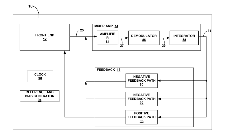
FIG. 7 is a block diagram illustrating instrumentation amplifier 10 in greater
detail. It
should be understood that FIG. 7 is merely exemplary and should not be
considered limiting
of the invention as described in this disclosure in any way. Rather, it is the
purpose of FIG. 7
to provide an overview that is used to describe the operation of
instrumentation amplifier 10
in greater detail. This overview is used as a framework for describing the
previously
mentioned example embodiments with respect to the detailed circuit diagrams
provided in
this disclosure.
22
CA 02675382 2009-07-13
WO 2008/094271 PCT/US2007/066358
In FIG. 7, front end 12 outputs a modulated differential input signa125. The
modulated differential input signal carries the signal of interest at a
carrier frequency. As
previously described, front end 12 may take the form of various different
components. Front
end 12 may, for example, be a continuous time switched capacitor network that
modulates
(chops) an input signal from a physiological sensor, an impedance sensor that
modulates a
stimulation current to produce an AC modulated signal that is AC coupled to
mixer amplifier
14 through tissue of a patient, or part of a telemetry transmitter that
modulates the data
encoded output signal to a carrier frequency for transmission over a wireless
channel. Thus,
it should be understood that front end 12 may be any component or combination
of
components that produces a differential modulated input signal as broadly
described in this
disclosure.
In particular, when implemented with a continuous time switched capacitor
network
coupled to a physiological sensor, the continuous time switched capacitor
network operates
as a modulator that modulates (chops) the differential signal output by the
physiological
sensor to a carrier frequency. The physiological sensor may be a set of
electrodes, an
accelerometer, a pressure sensor, a voltage sensor or other sensor that
outputs a differential
voltage signal. In particular, the physiological sensor may, for example,
generate a
differential signal proportional to physiological signals such as, ECG
signals, EMG signals,
EEG signals, or other signals. The differential signal generated by the sensor
is a low
frequency signal. Using physiological signals as an example, the frequency of
the
differential signal may be within a range of approximately 0 Hz to
approximately 100 Hz,
and may be less than approximately 2 Hz, and in some cases less than
approximately 1 Hz..
Sensors other than physiological sensors may also be used. That is, the sensor
does
not need to output a differential signal proportional to a physiological
signal. Rather, the
sensor may be any electrode, accelerometer, pressure sensor, voltage sensor or
other sensor
that outputs a differential signal, which may or may not represent a
physiological signal or
serve a medical sensing application. However, in the case of a physiological
sensor, the
carrier frequency may be within a range of approximately 4 kHz to
approximately 10 kHz,
although other frequencies are possible. It is important, however, that the
carrier frequency
be sufficiently higher than the frequency of the baseband signal of interest
and within a range
23
CA 02675382 2009-07-13
WO 2008/094271 PCT/US2007/066358
that does not introduce significant noise into the signal, i.e., a frequency
at which mixer
amplifier 14 operates without introducing noise into the signal.
In this case, the modulator in front end 12 may include a differential set of
switches,
e.g., CMOS switches, that are toggled between the outputs of the physiological
sensor to
modulate (chop) an amplitude of the input signal. Clock 96 supplies the clock
signal that the
modulator in the front end 12 and demodulator 86 in mixer amplifier 14 use to
modulate the
differential input signal at the carrier (chop) frequency. At one end, the
switches are cross
coupled to each other and toggle between the output terminals of the sensor to
reject common
mode signals and operate as continuous time process, i.e., a non-sampling
process. The
switches are coupled at the other end to input capacitors of mixer amplifier
14 to form a
continuous time switched capacitor network. In this way, front end 12
amplitude modulates
(chops) the differential input signal at the inputs to mixer amplifier 14.
Consequently, the
modulated differential input signal produced by front end 12 is a square wave
with a
frequency equal to the carrier frequency. A circuit diagram for this example
embodiment is
provided in FIG. 8.
When front end 12 is implemented as an impedance sensor, front end 12 may
include
a set of CMOS SPDT switches that are coupled at one end to reference
potentials and to
corresponding resistors at the other end. The switches toggle between the
reference
potentials and are cross-coupled to each other to modulate (chop) a
stimulation current
through the resistors and reject common-mode signals. The resistors may be
connected in
series to respective capacitors that are AC coupled to mixer amplifier 14
through tissue of a
patient. The chopped stimulation current produces a chopped voltage on the
tissue with an
amplitude modulated at the carrier frequency that is AC coupled to mixer
amplifier 14. A
circuit diagram is provided for this example embodiment in FIG. 9.
When instrumentation amplifier 10 is used to demodulate telemetry signals,
front end
12 may be viewed as part of a transmitter in the telemetry system. In
particular, front end 12
may be implemented using any circuitry known in the art of telemetry that
modulates a data
encoded signal to a carrier frequency for transmission over a wireless
channel. For example,
front end 12 may be viewed as part of a receiver located in an IPG that is
implanted within a
patient and communicates with a clinician or patient programmer.
Alternatively, front end
12 may be part of a receiver of the clinician or patient programmer that
communicates with
24
CA 02675382 2009-07-13
WO 2008/094271 PCT/US2007/066358
the IPG implanted within the patient. A detailed block diagram for this
example embodiment
is provided in FIG. 15A.
In any case, front end 12 generates a differential input signal for mixer
amplifier 14.
Noise, e.g., 1/f noise, popcorn noise, and offset, enters the signal path of
instrumentation
amplifier 10 at mixer amplifier 14 to produce noisy modulated input signa125.
Noisy
modulated input signa125 includes the original low frequency components
modulated up to
the carrier frequency and noise components at baseband.
As previously described, mixer amplifier 14 may be implemented using the
modified
folded-cascode amplifier architecture illustrated in FIG. 6. Reference and
bias generator 94
supplies bias and reference voltages to mixer amplifier 14. In the interest of
simplicity,
mixer amplifier 14 is illustrated in FIG. 7 as including amplifier 84,
demodulator 86, and
integrator 88, which correspond to amplifier 26, demodulator 28, and
integrator 30 in FIG. 2.
Accordingly, amplifier 84 amplifies noisy modulated input signa125 and
demodulator 86
demodulates amplified signa127. More specifically, demodulator 86 demodulates
the
original low frequency signal components of the amplified signal back down to
baseband and
modulates noise 23 up to the carrier frequency, thereby maintaining separation
between the
desired signal and noise. Clock 96 supplies a clock signal to drive
demodulator 86. For
example, with respect to the circuit diagram of FIG. 6, clock 96 supplies a
clock signal to
drive switches 60 and 62 which operate as demodulator 86. Integrator 88
integrates
demodulated signa129 with respect to a reference voltage supplied by reference
and bias
generator 94 and acts as a low pass filter that substantially eliminates
signal components with
a frequency outside of the baseband. Consequently, noise sitting at the
carrier frequency of
demodulated signa129 is substantially eliminated from the output of integrator
88, i.e., output
signa131.
In FIG. 7, feedback 16 includes negative feedback path 90, negative feedback
path
92, and positive feedback path 98. To provide a differential-to-single
conversion, each of
feedback paths 90, 92, and 98 may include two symmetrical feedback path
branches to
provide feedback to respective positive and negative differential inputs of
mixer amplifier 14.
In particular, negative feedback path 90 provides negative feedback at the
input to mixer
amplifier 14 to keep the signal change small. Each of the feedback path
branches of negative
feedback path 90 modulates output signa131 with a reference voltage provided
by reference
CA 02675382 2009-07-13
WO 2008/094271 PCT/US2007/066358
and bias generator 94. To ensure that a negative feedback path exists in
negative feedback
path 90 at all times, the chop frequency applied to the negative feedback path
branches of
feedback path 90 should be 180 degrees out of phase with each other with one
of the
feedback paths synchronous with front end 12. In this way, one of the feedback
path
branches of negative feedback path 90 is applying negative feedback during
each half of the
clock cycle. As a result, the differential signals at the input of mixer
amplifier 14 are small
and centered about the reference voltage. Negative feedback 90 substantially
eliminates the
dynamic limitation of instrumentation amplifier 10, i.e., glitching in output
signa131.
Negative feedback path 92 allows for the construction of a high pass filter.
In
particular, negative feedback path 92 integrates the output of instrumentation
amplifier 10,
i.e., output signa131, with respect to a reference voltage supplied by
reference and bias
generator 94 and applies the integrated signal to the inputs of mixer
amplifier 14 through a
capacitor. Each of the feedback path branches of negative feedback path 92
modulates the
integrated output signal with the reference voltage. Similar to the previously
described
feedback paths of negative feedback path 90, relative phasing of feedback path
branches of
negative feedback path 92 should ensure that a negative feedback path exists
for each half of
the clock cycle. In operation, negative feedback path 92 is dominant at low
frequency and
suppresses the DC response of instrumentation amplifier 10. However, negative
feedback
path 90 is dominant at passband frequencies. The scaling of feedback
capacitors in feedback
path 90 and the time constant of feedback path 92 set the high pass corner of
the filter. In
other words, capacitors in feedback paths 90 and 92 are used to set the high
pass corner.
As an example, a high pass filter may be useful for rejecting post-pacing
artifacts
when instrumentation amplifier 10 is used for heart monitoring applications
and filtering out
electrode offsets when instrumentation amplifier is used for monitoring brain
signals. As an
example, feedback path 92 may be used to construct a high pass filter with a
cutoff frequency
equal to approximately 2.5 Hz, 0.5 Hz, or 0.05 Hz. In this case, feedback path
92 may be
dominant at frequencies below cutoff frequencies of 2.5 Hz, 0.5 Hz, or 0.05
Hz, while
feedback path 90 may be dominant at frequencies above the cutoff frequencies.
In one
example, feedback path 92 may have a cutoff frequency of approximately .5 Hz,
permitting
feedback path 90 to dominate at frequencies above approximately .5 Hz, e.g.,
approximately
5 Hz to 100 Hz
26
CA 02675382 2009-07-13
WO 2008/094271 PCT/US2007/066358
Positive feedback path 98 increases the input impedance of instrumentation
amplifier
10. More specifically, positive feedback path 98 samples output signa131 and
provides
feedback to front end 12 before chopper modulation is applied to the input
signal. The
positive feedback effectively "replaces charge" on the input capacitors to
mixer amplifier 14
that is lost during the sampling process. Positive feedback path 98 may
increase the input
impedance of instrumentation amplifier 10 by an order of magnitude or more.
Each feedback
path branch of positive feedback path 98 may include a switched capacitor
arrangement to
add compensatory charge to the input capacitors.
Although FIG. 7 depicts feedback path 16 as including negative feedback path
90,
negative feedback path 92, and positive feedback path 98, only negative
feedback path 90
may be provided for instrumentation amplifier 10 to achieve stable
measurements at low
frequency with very low power. Accordingly, feedback paths 92, 98 may be
considered
optional, auxiliary feedback paths that enable instrumentation amplifier 10 to
achieve
additional performance enhancements. Consequently, various example embodiments
of the
invention described in this disclosure may include one, both, or neither of
feedback paths 92,
98. When the instrumentation amplifier includes feedback paths 92 and 98,
positive
feedback path 98 may sample the integrated output signal from negative
feedback path 92
instead of sampling the output signal of mixer amplifier 14. The relative
arrangement of
feedback paths 90, 92, 98 may be more apparent from the circuit diagrams that
follow in the
additional figures.
In some embodiments, clock 96 may comprise one or more clocks. For example,
when instrumentation amplifier 10 is implanted on a single chip, a single
clock may supply
clock signals to front end 12, mixer amplifier 14, and feedback path 16.
However, in some
embodiments, such as when instrumentation amplifier 10 is used to demodulate
telemetry
signals, front end 12 may be implemented on a separate chip than mixer
amplifier 14 and
feedback 16. In this case, front end 12 may be supplied with a clock signal
from one clock
while a different clock provides clock signals to mixer amplifier 14 and
feedback 16. In this
case, the two clocks may not be in phase with each other. Since the clocks
should be in
phase with each other to ensure that the transmitted signal can be recovered,
additional
circuitry may be required at the receiver to synchronize the clocks.
27
CA 02675382 2009-07-13
WO 2008/094271 PCT/US2007/066358
Reference and bias generator 94 supplies bias voltages to front end 12, mixer
amplifier 14, negative feedback path 90, and negative feedback path 92. When
front end 12
includes a physiological sensor, reference and bias generator 94 may supply
reference
voltages that drive the physiological sensor. Reference and bias generator 94
may also
supply the reference voltages to electrodes for an impedance sensor. With
respect to mixer
amplifier 14, reference and bias generator 94 may supply bias voltages for
biasing the
transistors as shown in FIG. 6. The reference voltages that are mixed with the
signals in
feedback paths 90 and 92 as previously described may also be supplied by
reference and bias
generator 94. Bias voltages of 0 volts to 1.2 volts (bandgap) or 0 volts to
0.6 volts (half
bandgap) may be used as bias points.
FIG. 8 is a circuit diagram illustrating an instrumentation amplifier 100.
Instrumentation amplifier 100 is an example embodiment of instrumentation
amplifier 10
previously described in this disclosure. In FIG. 8, instrumentation amplifier
100 includes
sensor 101 which generates a differential voltage across its outputs 102A and
102B
(collectively referred to as "outputs 102"). Outputs 102A and 102B provide
voltages Vin-
plus and Vin-minus, respectively. Sensor 101 may be a physiological sensor
that translates
biophysical signals to a differential electrical voltage across outputs 102.
For example,
sensor 101 may be an accelerometer, a pressure sensor, a force sensor, a
gyroscope, a
humidity sensor, a pair of electrodes, or the like.
Inputs 102A and 102B are connected to capacitors 106A and 106B (collectively
referred to as "capacitors 106") through switches 104A and 104B (collectively
referred to as
"switches 104), respectively. Switches 104 are driven by a clock signal
provided by a system
clock (not shown) and are cross-coupled to each other to reject common-mode
signals.
Capacitors 106 are coupled at one end to a corresponding one of switches 104
and to a
corresponding input of mixer amplifier 116 at the other end. In particular,
capacitor 106A is
coupled to the positive input of mixer amplifier 116, and capacitor 106B is
coupled to the
negative input of amplifier 116, providing a differential input.
In FIG. 8, sensor 101, switches 104, and capacitors 106 form front end 110.
Front
end 110 generally corresponds to front end 12 of instrumentation amplifier 10.
In particular,
front end 110 operates as a continuous time switched capacitor network as
previously
described with respect to front end 12. Switches 104 toggle between an open
state and a
28
CA 02675382 2009-07-13
WO 2008/094271 PCT/US2007/066358
closed state in which inputs 102 are coupled to capacitors 106 at a clock
frequency to
modulate (chop) the output of sensor 101 to the carrier (clock) frequency. As
previously
described, the output of sensor 101 may be a low frequency signal within a
range of
approximately 0 Hz to approximately 100 Hz. The carrier frequency may be
within a range
of approximately 4 kHz to approximately 10 kHz. Hence, the low frequency
sensor output is
chopped to the higher chop frequency band.
Switches 104 toggle in-phase with one another to provide a differential input
signal to
mixer amplifier 116. During a first phase of the clock signal, switch 104A
connects sensor
output 102B to capacitor 106A and switch 104B connects sensor output 102A to
capacitor
106B. During a second phase, switches 104 change state such that switch 104A
couples port
102A to capacitor 106A and switch 104B couples port 102B to capacitor 106B.
Switches
104 synchronously alternate between the first and second phases to modulate
the differential
voltage at outputs 102 at the carrier frequency. The resulting chopped
differential signal is
applied across capacitors 106, which couple the differential signal across the
inputs of mixer
amplifier 116.
Resistors 108A and 108B (collectively referred to as "resistors 108") provide
a DC
conduction path that controls the voltage bias at the input of mixer amplifier
116. In other
words, resistors 108 may be selected to provide an equivalent resistance that
is used to keep
the bias impedance high. Resistors 108 may, for example, be selected to
provide a 5 GS2
equivalent resistor, but the absolute size of the equivalent resistor is not
critical to the
performance of instrumentation amplifier 100. In general, increasing the
impedance
improves the noise performance and rejection of harmonics, but extends the
recovery time
from an overload. To provide a frame of reference, a 5 GS2 equivalent resistor
results in a
referred-to-input (RTI) noise of approximately 20 nV/rt Hz with an input
capacitance (Cin)
of approximately 25 pF. In light of this, a stronger motivation for keeping
the impedance
high is the rejection of high frequency harmonics which can alias into the
signal chain due to
settling at the input nodes of mixer amplifier 116 during each half of a clock
cycle.
It is important to note that resistors 108 are merely exemplary and serve to
illustrate
one of many different biasing schemes for controlling the signal input to
mixer amplifier 116.
In fact, the biasing scheme is flexible because the absolute value of the
resulting equivalent
resistance is not critical. In general, the time constant of resistor 108 and
input capacitor 106
29
CA 02675382 2009-07-13
WO 2008/094271 PCT/US2007/066358
may be selected to be approximately 100 times longer than the reciprocal of
the chopping
frequency.
Mixer amplifier 116 may produce noise and offset in the differential signal
applied to
its inputs. For this reason, the differential input signal is chopped via
switches 104A, 104B
and capacitors 106A, 106B to place the signal of interest in a different
frequency band from
the noise and offset. Then, mixer amplifier 116 chops the amplified signal a
second time to
demodulate the signal of interest down to baseband while modulating the noise
and offset up
to the chop frequency band. In this manner, instrumentation amplifier 100
maintains
substantial separation between the noise and offset and the signal of
interest. Mixer amplifier
116 and feedback path 118 process the noisy modulated input signal to achieve
a stable
measurement of the low frequency signal output by sensor 101 while operating
at low power.
As previously described, operating at low power tends to limit the bandwidth
of
mixer amplifier 116 and creates distortion (ripple) in the output signal.
Mixer amplifier 116
and feedback path 118 correspond to and, thus, operate in a manner similar to
previously
described mixer amplifier 14 and feedback path 16. More specifically, feedback
path 118
corresponds to negative feedback path 90 described in FIG. 7 Mixer amplifier
116 and
feedback path 118 substantially eliminate the dynamic limitations of chopper
stabilization
through a combination of chopping at low-impedance nodes and AC feedback,
respectively.
In FIG. 8, mixer amplifier 116 is represented with the circuit symbol for an
amplifier
in the interest of simplicity. However, it should be understood that mixer
amplifier 116 may
be implemented in accordance with the circuit diagram provided in FIG. 6.
Consequently,
mixer amplifier 116 provides synchronous demodulation with respect to front
end 12 and
substantially eliminates 1/f noise, popcorn noise, and offset from the signal
to output a signal
that is an amplified representation of the differential voltage produced by
sensor 101.
Without the negative feedback provided by feedback path 118, the output of
mixer
amplifier 116 would include spikes superimposed on the desired signal because
of the limited
bandwidth of the amplifier at low power. However, the negative feedback
provided by
feedback path 118 suppresses these spikes so that the output of
instrumentation amplifier 100
in steady state is an amplified representation of the differential voltage
produced by sensor
101 with very little noise.
CA 02675382 2009-07-13
WO 2008/094271 PCT/US2007/066358
Feedback path 118 in FIG. 8 may include two feedback paths that provide a
differential-to-single ended interface. The top feedback path branch modulates
the output of
mixer amplifier 116 to provide negative feedback to the positive input
terminal of mixer
amplifier 116. The feedback path branch includes capacitor 112A and switch
114A.
Similarly, the bottom feedback path branch of feedback path 118 includes
capacitor 112B
and switch 114B that modulate the output of mixer amplifier 116 to provide
negative
feedback to the negative input terminal of mixer amplifier 116. Capacitors
112A and 112B
are connected at one end to switches 114A and 114B, and at the other end to
the positive and
negative input terminals of mixer amplifier 116, respectively.
Switches 114A and 114B toggle between a reference voltage (Vref) and the
output of
mixer amplifier 116 to place a charge on capacitors 112A and 112B,
respectively. The
reference voltage may be, for example, a mid-rail voltage between a maximum
rail voltage of
amplifier 116 and ground. For example, if the amplifier circuit is powered
with a source of 0
to 2 volts, then the mid-rail Vref voltage may be on the order of 1 volt.
Importantly, switches
114A and 114B should be 180 degrees out of phase with each other to ensure
that a negative
feedback path exists during each half of the clock cycle. One of switches 114
should also be
synchronized with mixer amplifier 116 so that the negative feedback suppresses
the
amplitude of the input signal to mixer amplifier 116 to keep the signal change
small in steady
state. By keeping the signal change small and switching at low impedance nodes
of mixer
amplifier 116, e.g., as shown in the circuit diagram of FIG. 6, the only
significant voltage
transitions occur at switching nodes. Consequently, glitching (ripples) is
substantially
eliminated or reduced at the output of mixer amplifier 116.
Switches 104 and 114, as well as the switches at low impedance nodes of mixer
amplifier 116, may be CMOS SPDT switches. CMOS switches provide fast switching
dynamics that enables switching to be viewed as a continuous process. The
transfer function
of instrumentation amplifier 100 may be defined by the transfer function
provided in
equation (1) below, where Vout is the voltage of the output of mixer amplifier
116, Cin is the
capacitance of input capacitors 106, AVin is the differential voltage at the
inputs to mixer
amplifier 116, Cfb is the capacitance of feedback capacitors 112, and Vref is
the reference
voltage that switches 114 mix with the output of mixer amplifier 116.
31
CA 02675382 2009-07-13
WO 2008/094271 PCT/US2007/066358
Vout = Cin(AVin)/Cfb +Vref (1)
From equation (1), it is clear that the gain of instrumentation amplifier 100
is set by the ratio
of input capacitors Cin and feedback capacitors Cfb, i.e., capacitors 106 and
capacitors 112.
The ratio of Cin/Cfb may be selected to be on the order of 100. Capacitors 112
may be poly-
poly, on-chip capacitors or other types of MOS capacitors and should be well
matched, i.e.,
symmetrical.
Although not shown in FIG. 8, instrumentation amplifier 100 may include shunt
feedback paths for auto-zeroing amplifier 100. The shunt feedback paths may be
used to
quickly reset amplifier 100. An emergency recharge switch also may be provided
to shunt
the biasing node to help reset the amplifier quickly. The function of input
capacitors 106 is
to up-modulate the low-frequency differential voltage from sensor 101 and
reject common-
mode signals. As discussed above, to achieve up-modulation, the differential
inputs are
connected to sensing capacitors 106A, 106B through SPDT switches 104. The
phasing of the
switches provides for a differential input to the ac transconductance mixing
amplifier 116.
These switches 104 operate at the clock frequency, e.g., 4 kHz. Because the
sensing
capacitors 106 toggle between the two inputs, the differential voltage is up-
modulated to the
carrier frequency while the low-frequency common-mode signals are suppressed
by a zero in
the charge transfer function. The rejection of higher-bandwidth common signals
relies on
this differential architecture and good matching of the capacitors.
As further shown in FIG. 8, for applications in which measurements are taken
in
conjunction with stimulation pulses delivered by a cardiac pacemaker, cardiac
defibrillator,
or neurostimulator, blanking circuitry may be added to instrumentation
amplifier 100 the
inputs of mixer amplifier 116 and coupling capacitors 106 to ensure that the
input signal
settles before reconnecting mixer amplifier 116 to front end 110. For example,
the blanking
circuitry may be a blanking multiplexer (MUX) 111 that selectively couples and
de-couples
mixer amplifier 116 from front end 110. This blanking circuitry selectively
decouples the
mixer amplifier from the differential input signal and selectively disables
the first and second
modulators, i.e., switches 104, 114, e.g., during delivery of a stimulation
pulse.
Blanking MUX 111 is optional but may be desirable. The clocks driving switches
104, 114 to function as modulators cannot be simply shut off because the
residual offset
32
CA 02675382 2009-07-13
WO 2008/094271 PCT/US2007/066358
voltage on mixer amplifier 116 would saturate the amplifier in a few
milliseconds. For this
reason, blanking MUX 111 may be provided to decouple amplifier 116 from the
input signal
for a specified period of time during and following application of a
stimulation by a cardiac
pacemaker or defibrillator, or by a neurostimulator.
To achieve suitable blanking, the input and feedback switches 104, 114 should
be
disabled while mixer amplifier 116 continues to demodulate the input signal.
This holds the
state of the integrator within mixer amplifier 116 because the modulated
signal is not present
at the inputs of the integrator, while the demodulator continues to chop the
DC offsets.
Accordingly, blanking MUX 111 may further include circuitry or be associated
with circuitry
configured to selectively disable switches 104, 114 during a blanking
interval. Post blanking,
mixer amplifier 116 may require additional time to resettle because some
perturbations may
remain. Thus, the total blanking time includes time for demodulating the input
signal while
the input and switches 104, 114 are disabled and time for settling of any
remaining
perturbations. An example blanking time following application of a stimulation
pulse may
be approximately 8 ms with 5 ms for mixer amplifier 116 and 3 ms for the AC
coupling
components.
FIG. 9 is a circuit diagram illustrating an instrumentation amplifier 200 for
measuring
impedance across a tissue load 211. Tissue load 211 represents the tissue of a
patient for
which impedance is measured by instrumentation amplifier 200. Tissue 211 may
be organ
tissue, such as heart tissue, lung tissue, or brain tissue, muscle tissue,
adipose tissue, or other
tissue for which the impedance may be measured to diagnose chronic or acute
disease states
or other medical conditions. Some example applications for impedance
measurements
include detection of pulmonary edema, minute ventilation measurements for
respiration,
measurement of cardiac dynamics, and measurement of brain signals. In general,
it is
important that instrumentation amplifier 200 does not stimulate excitable
cells in the tissue or
cause other detrimental effects such as electrode corrosion.
Instrumentation amplifier 200 may generally conform to instrumentation
amplifier 10
described with reference to FIGS. 1-7. In the example of FIG. 9,
instrumentation amplifier
200 applies synchronous detection principles to accurately measure the
impedance of tissue
load 211 with low power, inherent charge balancing, rejection of electrode
potentials, and
small stimulation currents. Instrumentation amplifier 200 is an example
embodiment of
33
CA 02675382 2009-07-13
WO 2008/094271 PCT/US2007/066358
previously described instrumentation amplifier 10. Like instrumentation
amplifier 10,
instrumentation amplifier 200 includes a front end 210, mixer amplifier 226,
and feedback
path 228. These features may generally correspond to front end 12, mixer
amplifier 14, and
feedback path 16 of instrumentation amplifier 10.
In FIG. 9, front end 210 includes input voltages at ports 202A and 202B
(collectively
referred to as "ports 202"), switches 204A and 204B (collectively referred to
as "switches
204"), resistors 206A and 206B (collectively referred to as "resistors 206"),
and capacitors
208A and 208B (collectively referred to as "capacitors 208"). In general,
front end 210
modulates a stimulation current that creates a voltage on tissue load 211. The
stimulation
current may be applied across tissue load 211 via two or more electrodes,
which may be
mounted on one or more leads or carried on a surface of an implantable medical
device
housing. Similarly, the resulting voltage signal across tissue load 211 may be
sensed by two
or more electrodes deployed on one or more leads or on a device housing. The
voltage on
tissue load 211 is AC coupled to positive and negative inputs of mixer
amplifier 226 by
capacitors 222A and 222B (collectively referred to as "capacitors 222"),
respectively. Thus,
the tissue represented by tissue load 211 is not exposed to DC current.
Moreover, the small
modulated (AC) stimulation current, which may be approximately 10 A or less,
may not
substantially excite the tissue represented by tissue load 211.
Switches 204 toggle between input voltages at ports 202 (Vstim+ and Vstim-) to
generate stimulation current through resistor-capacitor (RC) pairs of resistor
206A and
capacitor 208A and resistor 206B and capacitor 208B. Switches 204, resistors
206 and
capacitors 208 may form an alternating current (ac) source that generates an
ac stimulation
current at a clock frequency for application to a load, such as 211. In
particular, switches
204, resistors 206 and capacitors 208 form a modulator that modulates first
and second
voltages Vstim+ and Vstim- at the clock frequency to produce the stimulation
current for
application to the load. However, other types of ac current sources may be use
to provide the
ac stimulation current for impedance measurement.
The input voltages Vstim+ and Vstim- may be provided by regulated power
supplies
within a device in which instrumentation amplifier 200 is employed, such as an
implantable
medical device. Switches 204 open and close at a chopper frequency to, in
effect, chop the
input stimulation current delivered by input voltages at ports 202 via the RC
pairs (206, 208)
34
CA 02675382 2009-07-13
WO 2008/094271 PCT/US2007/066358
to measure tissue impedance. In this manner, front end 210 generates a
modulated
differential input signal that is processed by mixer amplifier 226 and
feedback path 228.
Stimulation currents at ports 202 may be provided by electrodes carried on
leads that are
connected to an IPG implanted within a patient. This is one example of
delivery of
stimulation current for impedance measurements. As an alternative, stimulation
current for
impedance measurement could be generated by one or more switched current
sources. The
reference voltages at ports 202 and the sizes of resistors 206 and capacitors
208 may be
determined by the constraints on the stimulation current, linearity of the
measurement, and
the time constant of instrumentation amplifier 200 compared to the clock (not
shown) that
drives switches 204.
As an example, using a stimulation current of 10 A, voltages at ports 202A
and
202B may provide 2V and 0 V, respectively, and resistors 206 may be selected
as 100 kS2
resistors. Alternatively, using 2000 kS2 resistors yields a 0.5 A stimulation
current with 100
kS2 resistors. Using 10 nF capacitors for capacitors 208 results in a
stimulation current
having a time constant of 1 ms, which requires a stimulation current with a
frequency of
approximately 5 kHz to ensure minimal error from settling dynamics. The
nonlinearity of
the measurement, assuming 1 kHz loads, is bounded to under 0.5% in this case.
The input to mixer amplifier 226 may include a high pass filter 212 and
coupling
capacitors 222A, 222B. In some embodiments, high pass filter 212 assists in
keeping post-
pace recovery to a minimum for cardiac dynamic measurements. In FIG. 9, high
pass filter
212 includes capacitors 214A, 214B (collectively referred to as "capacitors
214") and
resistors 216A, 216B (collectively referred to as "resistors 216"). The values
of capacitors
214 and resistors 216 may be selected such that high pass filter 212 has a
high pass corner
frequency that ensures minimal phase error, e.g., less than 1% equivalent
measurement error,
occurs at mixer amplifier 226 while settling any residual pacing errors in 2.5
ms to 5 time
constants. For some applications, such as cardiac impedance analysis, the high
pass corner
frequency may, for example, be within a range of approximately 300 Hz to
approximately
800 Hz.
Resistors 224A and 224B (collectively referred to as "resistors 224") control
the
voltage at the input of mixer amplifier 226. Accordingly, resistors 224 are
similar to resistors
108 in FIG. 7 and are merely exemplary. As previously described, resistors 224
or a
CA 02675382 2009-07-13
WO 2008/094271 PCT/US2007/066358
different bias scheme may be selected to provide a 5 GS2 equivalent resistor
although the
absolute value is not critical.
Mixer amplifier 226 and feedback path 228 process the noisy modulated input
signal
to achieve a stable measurement of the differential voltage on tissue load 211
while operating
at low power. Mixer amplifier 226 and feedback path 228 generally correspond
to mixer
amplifier 116 and feedback path 118 in FIG. 7. Accordingly, mixer amplifier
226 provides
synchronous demodulation with respect to front end 12 and substantially
eliminates noise,
i.e., 1/f noise, popcorn noise, and offset, from the amplified output signal.
Mixer amplifier
226 may be implemented using the modified folded-cascode architecture with
switching at
low impedance nodes, e.g., substantially as shown in FIG. 6.
As shown in FIG. 9, feedback path 228 includes top and bottom feedback path
branches that provide negative feedback and a single-to-differential
interface. The top and
bottom feedback path branches include capacitors 230A and 230B (collectively
referred to as
"capacitors 230") which are connected to switches 232A and 232B (collectively
referred to
as "switches 232"), respectively. Switches 232A and 232B are 180 degrees out
of phase with
each other and toggle between the output of mixer amplifier 226 and a
reference voltage
(Vref) to modulate the output of mixer amplifier 226. Consequently, feedback
path 218
provides negative feedback to keep the signal change at the input to mixer
amplifier 226
small as previously described in this disclosure.
Switches 206, switches 232, and the switches at low impedance nodes in mixer
amplifier 226 may be CMOS SPDT switches or other switches that provide fast
switching
dynamics. The transfer function for instrumentation amplifier 200 is the same
as that for
instrumentation amplifier 100, which is provided in the above description of
FIGS. 7 and 8.
Thus, the ratio of the capacitance of feedback capacitors, i.e., capacitors
230, to the
capacitance of input capacitors, i.e., capacitors 222, sets the gain of
instrumentation amplifier
226. Capacitors 222 and 230 may be poly-poly capacitors or other types of MOS
capacitors
and should be well matched, i.e., symmetrical. Capacitors 222 and 230 may be
placed on
chip with the other instrumentation amplifier components.
In operation, instrumentation amplifier 200 may fold electromagnetic
interference
(EMI) into the modulated input signal at the carrier frequency and odd
harmonics. In order
to determine if the channel is corrupt, the output of instrumentation
amplifier 200 can be
36
CA 02675382 2009-07-13
WO 2008/094271 PCT/US2007/066358
monitored with no stimulation current applied to front end 210. Alternatively,
spread-
spectrum techniques may be used to break up the synchronous clock detection
between front
end 210 and mixer amplifier 226. Spread-spectrum clocking breaks up the
uncorrelated
noise into a broadband noise signal that is substantially eliminated by mixer
amplifier 226,
while maintaining the correlated impedance measurement.
The output of instrumentation amplifier 200 may be sent to an analog-to-
digital
converter (ADC) (not shown) that applies additional processing for measuring
the impedance
of tissue load 211. Further, when instrumentation amplifier 200 is implanted
within a
patient, the tissue-electrode interface (front end 12) may be galvanically
isolated from the
measurement circuit (mixer amplifier 226 and feedback path 228). Isolation
helps to reject
electrode polarization and ensure net charge balance across the electrodes.
Instrumentation amplifier 200 can be used to separate the measurement of lead
impedances from impedance measurements for edema, minute ventilation, and
cardiac
dynamics. The reason for this is that the requirements are different for the
two
measurements. Lead impedances ordinarily require a quick sample to be taken
just prior to
delivery of a pacing or stimulation pulse, with several vectors requiring
measurement.
Perturbation of the sensing channel is not a major issue since the stimulation
pulse
immediately follows the measurement. This favors the application of large,
fast, sampled
stimulation current. The measurement of edema, minute ventilation and cardiac
dynamics,
however, occur at low frequency where the sensing channel should be free of
perturbations
and noise. Significant perturbations from this measurement, i.e., measurement
of lead
impedances, compromises the ability of the sense channel to accurately detect
evoked
potentials post-pace and can result in oversensing. Edema, minute ventilation
and cardiac
dynamic measurements therefore favor low level stimuli, averaged with
continuous time
methods. Instrumentation amplifier 200 enables edema, minute ventilation and
cardiac
dynamic measurements to be separate from measurement of lead impedances.
Although not shown in FIG. 9, for applications in which measurements are taken
in
conjunction with stimulation pulses delivered by a cardiac pacemaker or
neurostimulator,
blanking circuitry such as the blanking MUX 111 shown in FIG. 8 may be added
to
instrumentation amplifier 200. For example, a blanking MUX may disconnect
input
capacitors 222 from the inputs of mixer amplifier 226. In addition, input and
feedback
37
CA 02675382 2009-07-13
WO 2008/094271 PCT/US2007/066358
modulators may be disabled during the blanking period. In some embodiments,
the blanking
MUX may be placed between high pass filter 212 and coupling capacitors 222 to
ensure that
the input signal settles before reconnecting mixer amplifier 226 to front end
210. Hence, the
blanking circuitry may be a multiplexer (MUX) that selectively couples and de-
couples
mixer amplifier 226 from front end 210. As mentioned with reference to FIG. 8,
blanking
circuitry may be desirable because the clocks driving the switches cannot be
simply shut off
since the residual offset voltage on mixer amplifier 226 would saturate the
amplifier in a few
milliseconds.
To achieve suitable blanking, the input and feedback switches 222, 232, should
be
disabled while mixer amplifier 226 continues to demodulate the input signal.
This holds the
state of the integrator within mixer amplifier 226 because the modulated
signal is not present
at the inputs of the integrator, while the demodulator continues to chop the
DC offsets. Post
blanking, mixer amplifier 226 may require additional time to resettle because
some
perturbations may remain. Thus, the total blanking time includes time for
demodulating the
input signal while the input and feedback switches are disabled and time for
settling of any
remaining perturbations. An example blanking time may be approximately 8 ms
with 5 ms
for mixer amplifier 226 and 3 ms for the AC coupling components.
Through experimentation, it has been found that the linearity of measurement
via
instrumentation amplifier 200 meets a theoretical limit of 0.05% for a 500 nA
stimulation
current and 1.5% for a 10 A stimulation current. The worst-case linearity is
at high
impedance, due to finite output impedance of mixer amplifier 226. In other
words, higher
stimulation currents result in greater non-linearity. In practice, the
observable nonlinearity is
small for reasonable stimulation vectors through a tissue load on the order of
1 M.
Experimentation has also shown the measured noise floor of an instrumentation
amplifier including a mixer amplifier and negative feedback, such as
instrumentation
amplifier 100 and 200, to be approximately 100 nV/rt Hz. This is in line with
theoretical
expectations form Johnson noise in the input transistors of the mixer
amplifier 226 operating
with 1 A of stimulation current. For a 10 A stimulation current, this
translates into an
equivalent noise floor of 0.01 ohms/rtHz, which is well below the requirements
in many
physiological applications.
38
CA 02675382 2009-07-13
WO 2008/094271 PCT/US2007/066358
FIG. 10 is a diagram illustrating an example signal flow for an
instrumentation
amplifier 300 that includes negative feedback for constructing a high pass
filter. With
respect to FIG. 2, the architecture of instrumentation amplifier 300 in FIG.
10 may be
substantially the same as that of instrumentation amplifier 10, but with the
addition of
negative feedback path 92. Accordingly, similar number components in FIG. 2
and FIG. 10
share similar functionality. In the interest of brevity and to avoid
redundancy, the signal flow
through front end 10, mixer amplifier 14 and feedback path 90 is not described
in detail.
Instead, the flow of output signa131 which is produced by mixer amplifier 14
through
negative feedback path 92 is described.
In general, negative feedback path 92 performs additional signal processing on
output
signa131 to construct a high pass filter at the input to mixer amplifier 14.
The high pass filter
substantially eliminates signal components that have a frequency below the
corner frequency
of the high pass filter. For example,, feedback path 92 may set a corner
frequency of
approximately equal to 2.5 Hz, 0.5 Hz, or 0.05 Hz. In general, negative
feedback path 92
suppresses signals between the corner frequency and DC. As previously
described, feedback
path 92 provides differential feedback to respective input terminals of mixer
amplifier 14
through symmetrical feedback paths. The feedback paths should be 180 degrees
out of phase
with each other so that negative feedback is applied during each half cycle of
the clock cycle.
As shown in FIG. 10, negative feedback path 92 includes an integrator 302 and
modulator 304. Integrator 302 integrates output signa131 with respect to a
reference voltage.
This reference voltage should be the same reference voltage that is modulated
with the signal
in instrumentation amplifier 300 by modulators 20, 28, and 34. In some
embodiments, a
switched capacitor integrator may be used for integrator 302. In other
embodiments, a
standard RC integrator may be used. The switched capacitor integrator may,
however,
provide certain advantages.
Modulator 304 modulates the output of integrator 302 to provide a differential
voltage
into mixer amplifier 14. Since modulator 304 should be synchronized with
feedback path 90,
clock signa121 C also drives modulator 304. Clock signa121 C is also supplied
to integrator
302, as shown in FIG. 10, when integrator 302 is implemented as a switched
capacitor
integrator. Also shown in FIG. 10 are input capacitance (Cin) 13, feedback
capacitance
(Cfb) 17 for feedback path 90, high pass filter capacitance (Chp) 10 for
feedback path 92.
39
CA 02675382 2009-07-13
WO 2008/094271 PCT/US2007/066358
In operation, integrator 302 produces a voltage on the switched capacitor of
modulator 304 that counters the charge on the switched capacitor of modulator
34. When an
input step is applied to mixer amplifier 14, the signal is integrated by
integrator 30. Initially,
the voltage difference between demodulated signa129 and the reference voltage
of integrator
30 is relatively large. In contrast, the difference between the voltage of
output signa131 and
the reference voltage for integrator 302 is relatively small. As a result,
integrator 30 builds
up charge on the switched capacitor of modulator 34 more quickly than
integrator 302 builds
up charge on the switched capacitor of modulator 304.
Over time, however, the voltage difference between demodulated signa129 and
the
reference voltage at integrator 30 decreases and integrator does not build up
as much charge.
At the same time, the voltage difference between output signa131 and the
reference voltage
at integrator 302 increases and integrator 302 builds up more charge on the
switched
capacitor at modulator 304. Thus, in steady state, feedback path 92 dominates
feedback path
90 and the feedback counter charge is mostly provided via negative feedback
path 92. As a
result, feedback path 92 can set the high pass corner through a ratio of
capacitors 17 and 19
(Cfb and Chp) and a time constant set by the capacitors and clock frequency of
integrator
302. Importantly, since instrumentation amplifier 300 may be implemented
entirely on a
single chip, off chip capacitors may not be needed for high pass filtering.
FIG. 11 is a circuit diagram illustrating instrumentation amplifier 300. As
shown in
FIG. 11, the architecture of instrumentation amplifier 300 is substantially
the same as that of
instrumentation amplifier 100, but with the addition of negative feedback path
92.
Accordingly, similar number components in FIG. 7 and FIG. 10 share the same
functionality.
The operation of these shared components is not described in the interest of
brevity and to
avoid redundancy. However, the operation of feedback path 92 is described.
Negative feedback path 92 taps off of the output of mixer amplifier 116 and
applies
negative feedback to the inputs of mixer amplifier 116. In the example of FIG.
11, integrator
302 is a switched capacitor integrator. Integrator 302 may be in addition to
the integrator and
demodulator provided within mixer amplifier 116. The switched capacitor
integrator includes
a capacitor 310 coupled between the output of amplifier 116 and ground via
switch 312A,
and between the negative input of amplifier 316 and ground via switch 312B.
Switch 312A
and 312B toggle at the chop frequency, but are out of phase with one another.
The clocking
CA 02675382 2009-07-13
WO 2008/094271 PCT/US2007/066358
frequency of switches 312A and 312B can be adjusted to set the time constant
of integrator
302. The positive terminal of amplifier 316 is coupled to a reference voltage
(Vref), which
may be the same reference voltage that is mixed with the signal at other
stages in
instrumentation amplifier 300. Capacitor 314 couples the output of amplifier
316 to the
negative terminal of amplifier 316.
The two feedback paths of feedback path 92 tap off of the output of integrator
302 to
provide negative feedback to mixer amplifier 116. In particular, the top
feedback path
branch modulates the output of integrator 302 to provide negative feedback to
the positive
terminal of mixer amplifier 116. The top feedback path branch includes
capacitor 320A and
switch 322A. Similarly, the bottom feedback path branch of feedback path 92
includes
capacitor 320B and switch 322B, which modulate the output of integrator 302 to
provide
negative feedback to the negative terminal of mixer amplifier 116.
Capacitors 320A and 320B are connected at one end to switches 322A and 322B,
and
to the positive and negative input terminals of mixer amplifier 116 at the
other end,
respectively. Switches 322A and 322B toggle between a reference voltage (Vref)
and the
output of mixer integrator 302 to place a charge on capacitors 320A and 320B,
respectively.
Switch 322A and 322B toggle 180 degrees out of phase with one another.
Importantly,
switches 322A and 322B should be synchronized with switches 114A and 114B,
respectively. In this way, a negative feedback path exists during each half
cycle of the clock
signal and is synchronized with the negative feedback path.
As previously described in FIG. 10, integrator 302 builds up a voltage that is
placed
on capacitors 320A and 320B (collectively referred to as "capacitors 320") by
switches 322A
and 322B (collectively referred to as "switches 322"). The charge on
capacitors 320 counters
the charge on capacitors 106 in steady state. More specifically, the charge on
capacitors 320
dominates the feedback path in steady state for low frequencies. Thus, current
substantially
flows through negative feedback path 92 at steady state and little or no
current flows through
negative feedback path 118. As a result, the ratio of feedback capacitors 112
and 320 and the
time-constant of integrator 302 sets the corner frequency of the high pass
filter provided by
negative feedback path 92. The corner frequency may be set to equal to
approximately 2.5
Hz, 0.5 Hz, or 0.05 Hz, or other desired frequencies. With feedback capacitors
112 on chip,
41
CA 02675382 2009-07-13
WO 2008/094271 PCT/US2007/066358
the high-pass filter characteristics can be dynamically changed to help with
recovery from an
overload or transient.
Switches 312 and 322 may be CMOS SPDT switches or other switches that provide
fast switching dynamics. Capacitors 310, 314, and 320 may be poly-poly
capacitors or other
types of MOS capacitors.
It should be understood that feedback path 92, as shown in FIG. 11, may be
generally
applied to an instrumentation amplifier as broadly described in this
disclosure. Accordingly,
instrumentation amplifier 300 should not be considered limiting in any way.
Instead,
instrumentation amplifier 300 is one of many example instrumentation
amplifiers that may
include a negative feedback path for constructing a high pass filter as
described in this
disclosure. For example, feedback path 92, as shown in FIG. 11, may be added
to
instrumentation amplifier 200 in FIG. 9.
FIG. 12 is a diagram illustrating an exemplary signal flow for an
instrumentation
amplifier 400 that includes a positive feedback path for increasing the input
impedance of the
instrumentation amplifier. The architecture of instrumentation amplifier 400
may be
substantially the same as that of instrumentation amplifier 10 with respect to
FIG. 2, but with
positive feedback path 98 included to provide additional signal processing.
Accordingly,
similar numbered components in FIG. 12 share the same functionality of those
in FIGS. 2
and 10. In the interest of brevity and to avoid redundancy, the signal flow
through front end
10, mixer amplifier 14, and feedback path 90 is not described in detail.
Instead, the flow of
output signa131 which is produced by mixer amplifier 14 through positive
feedback path 98
is described.
In general, positive feedback path 98 taps off of the output of mixer
amplifier 14 or
optionally the output of the integrator 302 in feedback path 92, if provided.
Positive
feedback path 98 provides feedback to front end 12 prior to modulator 20,
i.e., prior to
application of chopping input signa132. As shown in FIG. 12, positive feedback
path 98
includes a switched capacitor arrangement 404 (Cpos) that is driven by clock
signa121 C. In
particular, switched capacitor 404 is used to create a resistance that is
substantially equal to
the effective resistance at the input of instrumentation amplifier 400. The
effective input
resistance (Reff) of instrumentation amplifier is given in equation (2) below,
where the
frequency of clock signals 2lA-C is Fclock, and Cin is the capacitance of the
input capacitors
42
CA 02675382 2009-07-13
WO 2008/094271 PCT/US2007/066358
106A, 106B at modulator 20. Accordingly, the charge draw looking into
instrumentation
amplifier 400 is described by equation (3), where Q is the electric charge,
and AVin is the
change in voltage.
Reff = 1/(Fclock = Cin) (2)
dQ =Cin=Fclock=AVin (3)
df
Positive feedback path 98 compensates for the current passing through the
effective
resistance by "replacing" or putting charge back onto the switched input
capacitors 13 of
modulator 20. Because the output voltage of instrumentation amplifier 400
without feedback
path 98 is proportional to the differential input voltage multiplied by the
ratio of the
capacitance Cin of the input capacitors 106A, 106B of modulator 20 to the
capacitance Cfb
of the feedback capacitors 112A, 112B of modulator 34, switched capacitor
arrangement 404
(Cpos) samples output of mixer amplifier 14 and uses positive feedback to
replace the lost
charge. In other words, positive feedback path 98 injects current that
compensates for
current passing through the effective input resistance. Positive feedback path
98 may raise
the equivalent low frequency input impedance by an order of magnitude or more.
Positive feedback path 98 may also be used at the same time as positive
feedback
path 92. In this case, positive feedback path 98 may tap off of the output of
the integrated
signal output by positive feedback path 92. With respect to FIG. 10, positive
feedback path
98 could tap off of the output of integrator 302, rather than the output of
mixer amplifier 116.
FIG. 13 is a circuit diagram illustrating instrumentation amplifier 400. In
FIG. 13, the
architecture of instrumentation amplifier 400 is substantially identical to
that of
instrumentation amplifier 300, but with positive feedback path 98 tapping off
of the output of
mixer amplifier 116 and providing positive feedback to capacitors 106 of front
end 110.
Components that share number between FIGS. 13 and FIGS. 8 and 11 share the
same
functionality. Accordingly, the operation of these components is not described
in the interest
of brevity and to avoid redundancy. However, the operation of positive
feedback path 98 is
described.
43
CA 02675382 2009-07-13
WO 2008/094271 PCT/US2007/066358
In FIG. 13, positive feedback path 98 provides differential feedback through a
first
feedback path branch and a second feedback path branch. The first feedback
path branch
(top branch) modulates the output of mixer amplifier 116 to provide positive
feedback to the
positive input terminal of mixer amplifier 114. The first feedback path branch
(top branch in
FIG. 13) includes capacitor 410A, switch 412A, and switch 412B. Switch 412A
selectively
couples one side of capacitor 410A to either a reference voltage Vref or the
output of mixer
amplifier 116. Switch 412B selectively couples the other side of capacitor
410A to either
Vref or input port 102A of sensor 101. The second feedback path branch (bottom
branch in
FIG. 13) includes capacitor 410B and switch 412C. One side of capacitor 410B
is coupled to
ground. Switch 412C selectively couples the other side of capacitor 410B to
either the output
of mixer amplifier 116 or input port 102B of sensor 101.
Capacitors 410A and 410B are both coupled to the output of mixer amplifier 116
during a first clock phase. Thus, during the first clock phase, capacitors
410A and 410B
sample the output of mixer amplifier 116. One end of capacitor 410A is coupled
to Vref
during the first phase. During a second clock phase, capacitors 410A and 410B
are coupled
at one end to input ports 102A, 102B, respectively. At the other end, during
the second clock
phase, capacitor 410A is coupled to Vref, while capacitor 410B is coupled to
ground. The
sizes of capacitors 410A and 410B are selected according to the charged needed
to
compensate for the sampling of the input capacitors 106A, 106B during front
end
modulation. As an example, each capacitor 410A, 410B may have a capacitance
value that is
approximately twice the value of the feedback capacitance Cfb of each
respective feedback
capacitor 112A, 112B. Capacitors 410A, 410B may be provided on-chip for close
matching
to capacitors 106A, 106B and 112A, 112B.
In the second feedback path branch (bottom), charge is delivered to the front
end
switch 104b during a second clock phase, i.e., after the first clock phase in
which capacitor
410B is coupled to sample the output of mixer amplifier 116. Similarly, in the
first feedback
path branch (top), charge is delivered to front end switch 104A during the
second clock
phase. To create a differential charge transfer from the single ended output
of mixer
amplifier 116, a different switching scheme is employed in the first feedback
path branch
(top) than in the bottom feedback path branch). The clock frequency used to
actuate
switches 412A, 412B, 412C may be the same as the chopping frequency. The
reference
44
CA 02675382 2009-07-13
WO 2008/094271 PCT/US2007/066358
voltages used for feedback path 98, and particularly the reference voltages to
which capacitor
410A is coupled in phase 1 and phase 2, should match the reference voltage
used in feedback
path 118.
Switches 412A, 412B and 412C may be CMOS SPDT switches or other switches that
provide fast switching dynamics. Capacitors 410A and 410B may be poly-poly
capacitors or
other types of MOS capacitors, and may be formed on-chip with capacitors 112A,
112B,
106A and 106B.
As previously described, positive feedback path 98 may also be used with
negative
feedback path 92 at the same time. In this case, using FIG. 11 as a reference,
positive
feedback path 98 could sample off of the output of integrator 302. That is,
switches 412A
and 412C could be connected to the output of integrator 302 instead of the
output of mixer
amplifier 116.
FIG. 14A is a diagram illustrating the signal flow for an instrumentation
amplifier
500 that is used as part of a receiver 498 in a telemetry system.
Instrumentation amplifier
500 may be used, for example, as part of a receiver 498 in an implantable
pulse generator
(IPG), implantable drug delivery device, or other type of implantable medical
device (IMD)
implanted within a patient that communicates, via telemetry, with an external
programming
device, such as a clinician or patient programmer. In addition,
instrumentation amplifier 500
may also be located in an external programming device that communicates with
an IPG or
other type of IMD implanted within the patient. Receiver 498 may receive
signals from a
transmitter 499 associated with an IMD or external programmer. Receiver 498
and
transmitter 499 together form a telemetry system that makes use of an
instrumentation
amplifier 500 as described in this disclosure. As will be described, a first
chopper stage
resides in the transmitter 499 while a second chopper stage and feedback path
reside in
instrumentation amplifier 500 in receiver 498.
In general, instrumentation amplifier 500 may be implemented as part of
telemetry
circuitry in an IMD or programming device for an IMD that communicates using
"arms
length telemetry." Arms length telemetry (ALT) refers to telemetry over
distances of
approximately 10 cm or greater. For example, ALT may operate over a distance
of
approximately 50cm or a distance of approximately 1 meter. Accordingly, ALT
eliminates
the burden of placing a programming device directly over the IMD for
communication.
CA 02675382 2009-07-13
WO 2008/094271 PCT/US2007/066358
However, the signal level for ALT is on the order of hundreds of microvolts as
a result of the
signal level dropping off as a cubic power of distance between the programming
device and
the IMD. Consequently, ALT requires micropower circuits to extract the
transmitted signal
while suppressing or rejecting out of band aggressors, i.e., noise. Aggressors
include
stimulation loop aggressors and similar phenomena.
Instrumentation amplifier 500 may be configured to provide synchronous
demodulation for the detection of on-off-keyed (OOK) signals. As an example,
such signals
may be transmitted by transmitter 499 in a 175 kHz industry-scientific-medical
(ISM) band.
The chopper stabilized mixer amplifier described in this disclosure, i.e.,
mixer amplifier 14
with negative feedback path 90, can be implemented in instrumentation
amplifier 500 to
provide synchronous demodulation with very low offset and stable gain.
Moreover, the gain
of instrumentation amplifier 500 can be conveniently determined by on-chip
capacitor ratios,
i.e., the ratio of the capacitance of the feedback capacitors in negative
feedback path 90 to the
capacitance of the input capacitors. As shown in FIG. 14A, instrumentation
amplifier 500
also includes a clock synchronizer 502 to correct for phase mismatch between
clocks at the
transmitter 499 and receiver 498. Clock synchronizer 502 may include another
chopper
stabilized mixer amplifier in accordance with an embodiment of this
disclosure.
In one example embodiment, the received signals may be transmitted using on-
off
keying of a 175 kHz signal to send data between a programming device and the
IMD in
which a receiver 498 incorporating instrumentation amplifier 500 resides. The
175 kHz
signal falls within the ISM band. The data may be framed with a fixed interval
of 22 s to
provide a 4.4 kbps rate. The duty cycle of the signal within the frame
signifies whether the
data bit is a one or a zero.
It should be understood that instrumentation amplifier 500 is not limited to
the above
protocol. Instead, this protocol is one of many example protocols that may be
used for ALT.
Accordingly, instrumentation amplifier 500 and the signal flow for
instrumentation 500 in
FIG. 14A should be viewed as examples for broadly teaching how a chopper
stabilized
instrumentation amplifier 500 described in this disclosure can be used for
synchronous
demodulation of signals for arms length telemetry and, therefore, should not
be considered
limiting in any way.
46
CA 02675382 2009-07-13
WO 2008/094271 PCT/US2007/066358
The signal flow of instrumentation amplifier 500 in FIG. 14A begins with
transmitter
499, which includes modulator 520. Modulator 520 receives an input data
signa1532
containing data to be transmitted, and chops the input signal at a chopping
frequency defined
by clock signa1521A to produce an output signal for transmission to receiver
498 via
transmit antenna 501 and receiver antenna 503. Additional amplifier or filter
components
may be provided to permit transmission of the modulated signal produced by
modulator 520
In terms of an analog to the other instrumentation amplifier embodiments
described in this
disclosure, transmitter 499 and modulator 520 form, in effect, a front end 12
that provides the
first chopping stage for the signal flow. Hence, in this case, front end 12 of
the overall
instrumentation amplifier 500 is a transmitter 499 associated with a separate
device, e.g., an
IMD or programmer. The transmitter 499 produces a digital bit stream and
converts the
digital bit stream into an analog waveform (input signa1532) that is modulated
to the carrier
frequency, e.g., 175 kHz, by modulator 520 to produce wireless signa1533 for
transmission
over a wireless channel. The wireless channel, in this case, is the path of
the wireless signal
533 between the programming device and the IMD implanted within the patient.
Wireless signa1533 is received by receive antenna 502. Mixer amplifier 14
receives
a signa1525 from summing node 522. As previously described with respect to
FIGS. 2, 10
and 12, mixer amplifier 14 may include an amplifier 26, a demodulator 28, and
an integrator
30. Components with similar numbers in each of these figures may operate in a
similar
manner. For example, amplifier 26 amplifies input signa1525 to produce an
amplified
signal, i.e., amplified signa1527. Modulator 28 demodulates amplified
signa1527 at the chop
frequency to produce demodulated signa1529, which carries the original data
stream located
back at baseband and noise modulated up to 175 kHz. Integrator 30 suppresses
the signal
components that are out of band with the baseband components, thereby
producing output
signa1531 which is substantially free of noise 523.
As previously described with respect to FIG. 10, negative feedback path 90
provides
negative feedback that keeps the signal change at the input to mixer amplifier
14 small. In
particular, negative feedback path 90 includes modulator 34 which modulates
output signal
531 to produce a differential feedback signal that is added to the signal path
at summing node
522. Clock signa1521C drives modulator 34 to modulate output signa1531 at the
chopping
carrier frequency via feedback capacitor 17 (Cfb). Negative feedback path 90
may include
47
CA 02675382 2009-07-13
WO 2008/094271 PCT/US2007/066358
two feedback path branches that apply the negative feedback to the positive
and negative
input terminals of differential mixer amplifier 14. The feedback paths are out
of phase with
each other to ensure that a negative feedback path exists during each half of
the clock cycle.
In this way, mixer amplifier 14 provides a stable, low noise output while
operating at low
power.
In FIG. 14A, however, the clocks that provide clock signals 521A and 521B are
not
located in the same physical location. In particular, clock signa1521A is
provided by a clock
located in the transmitter 498 and clock signa1521B is located in
instrumentation amplifier
500 in receiver 499. Accordingly, clock signa1521B may not be synchronized
with clock
signa1521A. The phase shift between clock signals 521A, 521B may result in a
signal null
in demodulated signa1529 when the shift is 90 degrees, or a beat frequency
that makes
decoding the received signal very difficult if not impossible. Clock
synchronizer 503
corrects for the phase mismatch between clock signals 521A, 521B.
As shown in FIG. 14A, clock synchronizer 502 uses the received signal, i.e.,
input
signa1533 to correct for phase mismatch between clock signals 521A and 521B.
Clock
signa1521B is used by modulator 528 to chop amplified signa1527, and by
modulator 34 in
feedback path 90 to chop output signa1531 for feedback to summing node 522.
With clock
signa1521B and clock signa1521A substantially synchronized with each other,
decoder 504
can produce a digital bitstream from output signa1531. Decoder 504 may be a
slicer or
similar component that can convert an analog baseband signal into a digital
bitstream. For
example, decoder 504 may include a slicer formed from a comparator that
detects a level of
the output signal. The comparator may have a dynamic level adjustment to
account for
variations in the background noise floor. Mild hysteresis may be added to the
slicer to
prevent multiple triggers in the digital waveform for small amplitude
transitions over short
periods of time.
Clock synchronizer 502 may be implemented as a phase lock loop or other
component known in the radio frequency (RF) communication arts that corrects
for a phase
mismatch between the clocks at the transmitter and receiver. In one example
embodiment,
clock synchronizer 502 may include a chopper stabilized mixer amplifier as
described in this
disclosure. The chopper stabilized mixer amplifier can be used to derive the
mixer clock, the
clock that provides clock signa1521 B to mixer amplifier 14, from the received
signal thereby
48
CA 02675382 2009-07-13
WO 2008/094271 PCT/US2007/066358
eliminating the need for quadrature reconstruction. In other words, the core
feature of the
instrumentation amplifier described in this disclosure can be used as a key
building block in
clock synchronizer 502 for building a synchronous clock derived from the
received signal.
This core feature has been described in detail with respect to mixer amplifier
14 with
negative feedback 90.
Using a chopper stabilized mixer amplifier in clock synchronizer 502 to derive
the
clock signal may have several advantages. First, the mixer amplifier is
chopper stabilized,
providing minimal referred to the antenna offset (RTAO). This provides a clean
signal for
extracting the small amplitude received signals, which may be on the order of
100
microvolts. The use of feedback path 90 and a compensation network allows loop
dynamics
to be adjusted to suppress out-of-band transients while maintaining lock on
the received
signal. In addition, signal processing is achieved with the chopper mixer
elements, which
keep current drawn from a power supply to a minimum. For example, the net
standby
current for instrumentation amplifier 500 with no polling may be approximately
5 A or less
in some embodiments.
In summary, receiver 498 may have three major building blocks. The front end
at
antenna 503 is attached to two chopper stabilized mixers, one of which is used
in a phase-
lock loop 502 to derive the reference clock, and the other of which is used in
mixer amplifier
14 to translate the received signal to baseband, and amplify it while
suppressing out-of-band
aggressors. In general, a chopper-stabilized mixer amplifier is provided in
clock
synchronizer 502 as a linear mixer to operate as a phase detector in a voltage
controlled
oscillator (VCO), while the other chopper-stabilized mixer amplifier operates
as a linear
mixer to provide demodulation, amplification, and lowpass filtering for data
extraction. The
output of the in-phase mixer amplifier 14 is passed to decoder 504 for
digitization. The
architecture of FIG. 14A provides a synchronous demodulator that may be
capable of high
sensitivity to received signals in the transmission band while rejecting out-
of-band
aggressors. Low-power synchronous demodulation is made possible by the chopper-
stabilized mixer architecture, which may be used in mixer amplifier 14 and
clock
synchronizer 502.
FIG. 14B is a circuit diagram illustrating input and feedback circuitry for
the
telemetry-configured instrumentation amplifier of FIG. 14A. As shown in FIG.
14B, mixer
49
CA 02675382 2009-07-13
WO 2008/094271 PCT/US2007/066358
amplifier 14 receives a modulated differential input signal via input
capacitors 106A, 106B
(Cin). Input capacitor 106A feeds a positive end of the differential antenna
signal (ANT+) to
the positive input of mixer amplifier 14. Input capacitor 106B feeds a
negative end of the
differential antenna signal (ANT-) to the negative input of mixer amplifier
14. Resistors
108A, 108B may be provided to set the inputs of mixer amplifier 14 to set an
input bias
impedance. Positive and negative inputs of mixer amplifier 14 may be coupled
to feedback
path branches of feedback path 90 via feedback capacitors 112A, 112B (Cfb) and
switches
114A, 114B, as in other embodiments. The capacitance of the feedback capacitor
112 (Cfb)
in relation to the capacitance of the input capacitor 106 (Cin) sets the
nominal gain of the
overall instrumentation amplifier. As in other embodiments, negative feedback
path 92 also
may be provided to set a highpass cutoff for the instrumentation amplifier.
FIG. 15A is a block diagram illustrating instrumentation amplifier 500. In
accordance with this disclosure, instrumentation amplifier 500 is illustrated
in FIG. 15A as
including mixer amplifier 14 and feedback path 16. Unlike the previously
described
embodiments, however, front end 12 is in a different physical location,
consistent with FIGS.
14A and 14B. In particular, as described with reference to FIG. 14A, front end
12 resides
within a transmitter 499 in a remote IMD or programmer. The signal received by
receive
antenna 503 of instrumentation amplifier 500 has already been chopped at the
remote IMD or
programmer. Instrumentation amplifier 500 includes clock synchronizer 502
which corrects
for the phase mismatch between the clock that drives front end 12 in the
remote device and
the clock that drives mixer amplifier 14. Clock synchronizer 502 provides a
linear mixer that
extracts the phase reference for use in the data demodulation path provided by
mixer
amplifier 14.
As shown in FIG. 15A, receive antenna 503 receives the wireless signal output
by the
remote transmitter. Mixer amplifier 14 of instrumentation amplifier 500
operates as
previously described and may be implemented as a modified folded cascode
amplifier with
switching at low impedance nodes. Thus, mixer amplifier 14 is illustrated in
FIG. 15A as
including amplifier 26, demodulator 28, and integrator 30. In FIG. 15A, mixer
amplifier 14
receives modulated input signa1525 from receive antenna 503. Amplifier 26
amplifies
modulated input signa1525 to produce amplified signa1527. Demodulator 28
demodulates
amplified signa1527 to produce demodulated signa1529 using switching at low
impedance
CA 02675382 2009-07-13
WO 2008/094271 PCT/US2007/066358
nodes of the folded cascode amplifier. However, demodulated signa1529 may
experience
signal nulls or a beat frequency unless the clock driving demodulator 28 is
synchronized with
the clock driving the modulator at the transmitter. This is the reason that
instrumentation
amplifier includes clock synchronizer 502.
Demodulated signa129 may contain 1/f noise, popcorn noise, and offset at the
carrier
frequency (175 kHz) and the original signal content at baseband. Integrator 30
integrates
demodulated signa1529 to produce output signa1531. In particular, integrator
30 integrates
demodulated signa1529 with respect to a reference voltage provided by a
receiver reference
and bias generator and acts as a low pass filter to suppress signal components
with a
frequency outside of the baseband. Consequently, noise sitting at the carrier
frequency of
demodulated signa1529 is substantially eliminated to produce a stable, low
noise output
signa1531.
Again, output signa1531 is stable because of the negative feedback provided by
negative feedback path 90. Without negative feedback path 90, output signa1531
includes a
series of spikes superimposed on the desired signal that make it very
difficult to slice the
signal into a digital bitstream and decode the data. These spikes are a result
of operating with
very low power which limits the bandwidth of mixer amplifier 14. Providing
negative
feedback at the input to mixer amplifier 14 keeps the signal change small in
steady state so
that the only significant voltage transitions occur at switching nodes.
Negative feedback path
90 includes symmetrical feedback path branches to provide the negative
feedback to
respective positive and negative differential inputs of mixer amplifier 14.
Each feedback
path branch modulates output signa1531 with a reference voltage provided by a
receiver bias
and reference voltage generator. The feedback path branches are 180 degrees
out of phase
with each other provide feedback during each half of the clock cycle. In this
way, mixer
amplifier 14 and negative feedback path 90 substantially eliminate glitching
to provide
stable, low noise output signa1531.
Output signa1531 may experience signal nulls or a beat frequency if the
transmitter
clock and receiver clock are not in phase with each other. The transmitter
clock signal drives
the modulator that modulates the baseband signal to the carrier frequency,
e.g., 175 kHz.
The receiver clock supplies a clock signal to mixer amplifier 14 and negative
feedback path
90. More specifically, the receiver clock supplies the clock signal that
drives demodulator 28
51
CA 02675382 2009-07-13
WO 2008/094271 PCT/US2007/066358
to demodulate the received, amplified signa1527 and the signal(s) that drive
modulation of
the output signa1531 in negative feedback path 90.
Clock synchronizer 502 corrects for the phase mismatch between the transmitter
clock and the receiver clock. In particular, clock synchronizer builds a
synchronous clock
derived from the received signal, i.e., modulated input signa1525, to produce
a correction
signal that is used by demodulator 28 in mixer amplifier 14 and the modulator
in negative
feedback path 90 to compensate for the phase mismatch.
Clock synchronizer 502 in FIG. 15A avoids problems that may be associated with
using a comparator to derive the mixer clock from the received signal. The
problems
associated with using a comparator may include difficulty producing a square
wave because
of the low power received signal. That is, it may be difficult for a
comparator to square up
millivolt signals at the 175 kHz clock frequency. The comparator also
typically requires an
AC coupled preamplifier or other mechanism for removing DC offsets on the
front-end,
which would otherwise lead to a significant duty cycle error and/or dead zone
for signals on
the order of millivolts or less. Further, a comparator has no memory and,
therefore, any
signal crossing results in the signal mixing into the baseband. This is a
problem with signals
on the order of hundreds of millivolts and, more particularly, signals on the
order of hundreds
of microvolts with sensitivity at the 175 kHz ISM band.
In FIG. 15A, clock synchronizer 502 operates as a phase lock loop and includes
chopper stabilized mixer amplifier 560, compensation network 562, voltage
controlled
oscillator (VCO) 564, and delay units 566 and 568. Mixer amplifier 560
includes a mixer
amplifier, arranged in a manner similar or identical to mixer amplifier 14.
Instead of
receiving negative feedback to the inputs of the mixer amplifier, however,
mixer amplifier
560 receives a quadrature phase clock feedback that is applied to a
demodulator in mixer
amplifier 560. Hence, in some embodiments, chopper stabilized mixer amplifier
560 may
include similar components and operate similar to mixer amplifier 14 described
in this
disclosure. For example, chopper stabilized mixer amplifier 560 may include,
with respect to
FIG. 15A, an amplifier, a demodulator, and an integrator that form a mixer
amplifier and be
coupled to receive a negative feedback path that provides the chopper
stabilization for
producing a stable output. As mentioned above, however, the negative feedback
received by
mixer amplifier 560 may be a quadrature phase feedback to adjust the clock
frequency of the
52
CA 02675382 2009-07-13
WO 2008/094271 PCT/US2007/066358
demodulator. The quadrature phase feedback is out of phase with the input
signal received
by mixer amplifier 560. Thus, chopper stabilized mixer amplifier 560 includes
a mixer
amplifier having the modified folded cascode amplifier architecture with
switching at low
impedance nodes. This architecture is illustrated in FIG. 6. Chopper
stabilized mixer
amplifier 560 is illustrated as a single block in FIG. 15A.
In general, clock synchronizer 502 provides a feedback path between its output
and
demodulator 28 of mixer amplifier 14. Chopper stabilized mixer amplifier 560
receives
modulated input signa1525 from receive antenna 503 and produces a stable, low
noise signal.
Importantly, chopper stabilized mixer amplifier 560 substantially removes
offset from the
received signal and outputs a signal that substantially or closely
approximates a square wave.
As a result, chopper stabilized mixer amplifier 560 may avoid the previously
discussed
problems associated with using a comparator.
Compensation network 562 receives the output of chopper stabilized mixer
amplifier
560 and applies an integrator and high-pass zero. By using an integrator in
compensation
network 562, the output adjusts VCO 564 such that the feedback clock (output
of VCO 564)
is in quadrature with the received signal. In other words, because zero net
signal is output by
chopper stabilized mixer amplifier 560 in steady state, the transmitter clock
and the output of
VCO 564 are in quadrature. The key is that by using an integrator in
compensation network
562, the integrator holds the VCO value while the received signal is in the
"off state" (output
of chopper stabilized mixer amplifier 560 still zero since signal is gone),
and reacquires the
VCO quickly when the signal goes high again. In this way, clock synchronizer
502 can be
viewed as a "phasor fly wheel" that is locked onto the received signal, i.e.,
modulated input
signa125, in quadrature.
VCO 564 may operate at approximately 350 kHz (2 * 175kHz ISM frequency) for
the
purpose of this example embodiment. The output of VCO 564 is processed by
delay units
566 and 568 to provide quadrature signals to the chopper stabilized mixer
amplifier 560,
demodulator 28, and the demodulator in negative feedback path 90. Delay unit
568 feeds the
output of VCO 564 back to the demodulator of chopper stabilized mixer
amplifier 560.
Delay unit 566 is tied to the opposite phase of VCO 564 to create an in-phase
clock for
demodulator 28 and negative feedback path 90. That is, because the output of
VCO 564 is
locked onto the input signal in quadrature, delay unit 566 introduces delay of
half a clock
53
CA 02675382 2009-07-13
WO 2008/094271 PCT/US2007/066358
cycle to create an in-phase clock for mixer amplifier 14 (demodulator 28) and
negative
feedback path 90. Hence, delay unit 566 is configured to feed the output of
VCO 564 with a
first phase (D to demodulator 28 of mixer amplifier 14 and modulator 34 of
negative feedback
path 90, while delay unit 568 is configured to feed the output of VCO 564 with
a second
phase of V to the demodulator in mixer amplifier 560. The outputs of delay
units 566 and
568 are 90 degrees out of phase with one another. With demodulator 28 using a
clock signal
that is in phase with the transmitter clock, signal processing can be applied
to the output of
mixer amplifier 14 to recover and decode the transmitted bits. Delay units 566
and 568 may
be D-type flip flops or other components that can be used to introduce delay
into the signal.
In general, clock synchronizer 502 may be a phase-locked-loop that extracts
the phase
reference for the data demodulation path of mixer amplifier 14 and negative
feedback path
90. The feedback from VCO 564 adjusts the modulation clock of chopper
stabilized mixer
amplifier 560 such that it is 90 degrees out of phase with the clock frequency
of the input
signa1525. In this case, chopper stabilized mixer amplifier 560 may act as a
linear phase
detector having an output that scales as Vin*cos((D), where Vin is the input
voltage from
receive antenna 503, and (Dis the phase difference between the chopper
stabilized mixer
amplifier 560 and the input signal. The resulting transfer function has a null
at 90 degrees.
For purposes of feedback compensation, small variations about that point can
be
approximated as a linear relationship.
The compensation of VCO 560 by compensation network 562 may be complicated by
the fact that loop gain scales with the input voltage. By using a simple
integrator with a zero
in compensation network 562, a stable phase lock can be obtained for small
signals at the
antenna 503. For large voltages, however, the compensation zero creates a
large signal at the
clock frequency that can saturate the channel and throw off the VCO. The
origin of this
signal is the "hidden state" of the mixer output at lock, which has no DC
component, but a
significant signal at the mixer frequency. To eliminate this problem, a second
pole can be
added to the compensation network 562 beyond loop cross-over. The purpose of
this pole is
to suppress the signal at the mixer frequency and minimize VCO jitter. As long
as the loop
gain is not too high, the additional pole should not be a problem. The extra
pole is pulled
into the compensation zero, which acts to pull the double integrator (one from
the mixer
54
CA 02675382 2009-07-13
WO 2008/094271 PCT/US2007/066358
amplifier 560 and one from the phase integration of VCO 564) off the imaginary
axis and
into the left half plane.
As VCO 564 is carefully compensated, a robust lock can be achieved across the
dynamic range of the telemetry link. In this way, the loop may be optimally
compensated in
that it responds more slowly and therefore more heavily filters disturbances
as the telemetry
link distance increases and signals fall off. In practice, a mode switch
driven by received
signal strength (RSSI) may be provided to maintain somewhat uniform dynamics
over a
typical telemetry link range. The mode switch may operate to adjust the loop
gain of clock
synchronizer 502 based on the level of the input signal. Hence, the loop gain
may be
decreased for higher input signal levels and increased for lower input signal
levels.
FIG. 15B is a block diagram illustrating a clock synchronizer 502 in FIG. 15A
in
greater detail. FIG. 15B illustrates clock synchronizer 502 substantially as
shown in FIG.
15A, but further illustrates example components of mixer amplifier 560. In
particular, mixer
amplifier 560 may include amplifier 26B, modulator 28B, and integrator 30B,
all of which
may function in a manner similar to amplifier 26, modulator 28 and integrator
30 of mixer
amplifier 14. As shown in FIG. 15B, however, delay unit 568 feeds the output
of VCO 564
in quadrature phase with input signa1525 to adjust modulator 28B of mixer
amplifier 560.
Hence, the feedback signal for modulator 28B is 90 degrees out of phase with
the input
signa1525, and is used to adjust the clock frequency of modulator 28B and
thereby maintain
chopper stabilization of mixer amplifier 560.
FIG. 16 is a block diagram illustrating various components of an implantable
medical
device (IMD) 700 including an instrumentation amplifier as described in this
disclosure.
IMD 700 includes therapy delivery module 702, processor 704, memory 708,
telemetry
module 706, sensor 710, power source 712, and therapy elements 714. In
general, IMD 700
includes a chopper stabilized instrumentation amplifier as part of sensor 710,
telemetry
module 76, or both.
Sensor 710 may be a pressure sensor, accelerometer, activity sensor, impedance
sensor, electrical signal sensor or other sensor configured to monitor heart
sounds, brain
signals, and/or other physiological signals. Although illustrated in FIG. 16
as contained
within IMD 700, a portion of sensor 710 may be located outside of IMD 700. For
example, a
sensor transducer or one or more electrodes may be located on a distal tip of
a lead implanted
CA 02675382 2009-07-13
WO 2008/094271 PCT/US2007/066358
at a target site within the patient and electrically coupled to IMD 700 via
conductors.
Alternatively, a sensor transducer or one or more electrodes may be provided
on or within a
housing of IMD 700. For example, an accelerometer may be provided within an
IMD
housing or within a lead that extends from the IMD. To sense electrical
signals, sensor 710
may include two or more electrodes arranged on a lead, an electrode on a lead
and an
electrode on an IMD housing, two or more electrodes arranged on an IMD
housing, or other
electrode arrangements. Sensor circuitry associated with sensor 710 may be
provided within
sensor 710 in the housing of IMD 700.
In general, sensor 710 provides a measurement of a physiological signal or
parameter
by translating signal or parameter to an output voltage or current. A chopper
stabilized
instrumentation amplifier amplifies and filters the sensor output as described
in this
disclosure to produce a stable, low noise signal with very low power
requirements. In this
way, the chopper stabilized instrumentation amplifier may enable IMD 700 to
operate for
several months or years relying on power from a finite power source 712, such
as a
rechargeable or nonrechargeable battery. In either case, power conversation is
desirable.
The output of sensor 710 and, more particularly, the output of the chopper
stabilized
instrumentation amplifier associated with sensor 710 may be received by
processor 704.
Processor 704 may apply additional processing, e.g., convert the output to
digital values for
processing, prior to storing the values in memory 708, and/or transmitting the
values to an
external programmer via telemetry module 706. Telemetry module 706 also may
include at
least a portion of a chopper-stabilized instrumentation amplifier. Processor
704 may also
control delivery of therapy to the patient based on the output of sensor 710.
IMD 700 may deliver therapy to a patient via therapy elements 714. In other
embodiments, IMD 700 may be dedicated to sensing and may not include therapy
delivery
module 702. Therapy delivery elements 714 may be electrodes carried on one or
more leads,
electrodes on the housing of IMD 700, one or more fluid delivery devices, or
any
combination thereof. Accordingly, therapy delivery module 702 may include an
implantable
stimulation generator or other stimulation circuitry that delivers electrical
signals, e.g., pulses
or substantially continuous signals, such as sinusoidal signals, to the
patient via at least some
of the electrodes that form therapy elements 714 under the control of
processor 704.
56
CA 02675382 2009-07-13
WO 2008/094271 PCT/US2007/066358
The stimulation energy generated by therapy delivery module 40 may be
formulated
as stimulation energy for treatment of any of a variety of cardiac or
neurological disorders, or
disorders influenced by patient neurological response. Example stimulation
therapies include
cardiac pacing, cardiac defibrillation, deep brain stimulation (DBS), spinal
cord stimulation
(SCS), peripheral nerve field stimulation (PNFS), pelvic floor stimulation,
gastrointestinal
stimulation, and the like.
Therapy delivery module 702, processor 704, telemetry module 706, memory 708,
and sensor 710 receive operating power from power source 712. Power source 712
may take
the form of a small, rechargeable or non-rechargeable battery, or an inductive
power interface
lo that transcutaneously receives inductively coupled energy. In the case of a
rechargeable
battery, power source 712 similarly may include an inductive power interface
for
transcutaneous transfer of recharge power.
In embodiments in which one or more fluid delivery devices are part of therapy
elements 714, therapy delivery module 702 may include a one or more fluid
reservoirs and
one or more pump units that pump fluid from the fluid reservoirs to the target
site through the
fluid delivery devices. The fluid reservoirs may contain a drug or mixture of
drugs. The
fluid reservoirs may provide access for filling, e.g., by percutaneous
injection of fluid via a
self-sealing injection port. The fluid delivery devices may comprise, for
example, catheters
that deliver, i.e., infuse or disperse, drugs from the fluid reservoirs to the
same or different
target sites.
Processor 704 may include a microprocessor, microcontroller, digital signal
processor
(DSP), application specific integrated circuit (ASIC), field programmable gate
array (FPGA),
discrete logic circuitry, or a combination of such components. Processor 704
is programmed
to control delivery of therapy according to a selected parameter set stored in
memory 708.
Specifically, processor 704 controls therapy delivery module 702 to deliver
electrical
stimulation, drug therapy, or a combination of both. For example, processor
704 may control
which drugs are delivered and the dosage of the drugs delivered.
Processor 704 may also control therapy delivery module 702 to deliver
electrical
stimulation with pulse amplitudes, pulse widths, and frequencies (i.e., pulse
rates) specified
by the programs of the selected parameter set. Processor 704 may also control
therapy
delivery module to deliver each pulse according to a different program of the
parameter set.
57
CA 02675382 2009-07-13
WO 2008/094271 PCT/US2007/066358
In some embodiments, processor 704 may control therapy delivery module 702 to
deliver a
substantially continuous stimulation waveform rather than pulsed stimulation.
Memory 708 may store parameter sets that are available to be selected by the
patient
for delivery of electrical stimulation and/or drug therapy. Memory 42 may also
store
schedules. Memory 708 may include any combination of volatile, non-volatile,
removable,
magnetic, optical, or solid state media, such as read-only memory (ROM),
random access
memory (RAM), electronically-erasable programmable ROM (EEPROM), flash memory,
or
the like.
Processor 704 also controls telemetry module 706 to exchange information with
an
external programmer, such as a clinician programmer and/or patient programmer
by wireless
telemetry. Processor 704 may control telemetry module 706 to communicate with
the
external programmer on a continuous basis, at periodic intervals, or upon
request from the
programmer. In addition, in some embodiments, telemetry module 706 may support
wireless
communication with one or more wireless sensors that sense physiological
signals and
transmit the signals to IMD 700.
Telemetry module 706 may operate as a transceiver that receives telemetry
signals
from an external programmer and transmits telemetry signals to an external
programmer. In
some embodiments, telemetry module 706 may include a chopper stabilized
instrumentation
amplifier. More specifically, with respect to FIGS. 14 and 15, the receiver
portion of
telemetry module 706 may include the back end of a chopper stabilized
instrumentation
amplifier, referred to as a chopper stabilized mixer amplifier and feedback
path, that
produces a baseband signal from a received telemetry signal. The receiver
portion is
described in this disclosure as including only the back end (chopper
stabilized mixer
amplifier) because the corresponding front end is located in the transmitter
portion of the
external programmer in communication with IMD 700.
The receiver portion may also include a clock synchronizer that includes
another
chopper stabilized mixer amplifier, e.g., as described with reference to FIG.
15A. This
chopper stabilized mixer amplifier produces an output that can be used by a
phase lock loop
to generate a correction signal that is used to synchronize the receiver
portion of telemetry
module 706 with the transmitter of the external programmer.
58
CA 02675382 2009-07-13
WO 2008/094271 PCT/US2007/066358
Telemetry module 706 also may include a transmitter to transmit signals from
IMD
700 to an external programmer or to another IMD or external medical device.
The
transmitter may include a front end of a chopper-stabilized instrumentation
amplifier in the
sense that it may include a first chopper stage that modulates an input signal
with an RF
frequency for transmission to an external programmer or another implanted or
external
medical device.
Importantly, the instrumentation amplifiers in sensor 710 and telemetry module
706
are micropower circuits that provide stable, low noise signals. Thus, IMD 700
may operate
over a longer duration of time than would be possible using instrumentation
amplifiers that
require more power for operation.
FIG. 17 is a block diagram illustrating an example patient or clinician
programmer
720 that allows a patient or clinician to communicate with IMD 700. A patient
or clinician
may interact with programmer 720 to program therapy, e.g., electrical
stimulation, drug
therapy, or a combination of both. In the illustrated example, programmer 720
includes
processor 722, user interface 724, input/output 726, telemetry module 728,
memory 730, and
power source 732. Programmer 720 may include a chopper stabilized
instrumentation
amplifier as part of telemetry module 728.
A patient or clinician, referred to as a user herein, may interact with
processor 722 via
user interface 724 in order to control delivery of electrical stimulation,
drug therapy, or a
combination of both. User interface 724 may include a display and a keypad,
and may also
include a touch screen or peripheral pointing devices as described above.
Processor 722 may
also provide a graphical user interface (GUI) to facilitate interaction with
the user, as will be
described in greater detail below. Processor 722 may include a microprocessor,
a controller,
a DSP, an ASIC, an FPGA, discrete logic circuitry, or the like.
Programmer 720 also includes memory 730. In some embodiments, memory 730
may store parameter sets that are available to be selected by the user for
delivery of therapy.
Memory 730 may also store schedules. Hence, parameter sets and schedules may
be stored
in IMD 700, programmer 720, or both. Programmer 720 also includes a telemetry
module
728 that allows processor 722 to communicate with IMD 700, and, optionally,
input/output
circuitry module 726 that allows processor 722 to communicate with another
programmer.
59
CA 02675382 2009-07-13
WO 2008/094271 PCT/US2007/066358
Processor 722 may receive parameter set selections made by the user via user
interface 724, and may either transmit the selection or the selected parameter
set to IMD 700
via telemetry circuitry 728 to deliver therapy according to the selected
parameter set. Where
programmer 720 stores parameter sets in memory 730, processor 722 may receive
parameter
sets from another programmer via input/output module 726 during programming by
a
clinician. For example, a patient programmer may receive parameter sets from a
clinician
programmer.
Telemetry module 728 may include a transceiver for wireless communication,
appropriate ports for wired communication or communication via removable
electrical
media, or appropriate drives for communication via removable magnetic or
optical media. If
wireless communication is used, telemetry module 728 may support both wireless
communication with IMD 700 and wireless communication with another programmer.
Similar to telemetry module 706 of IMD 700, telemetry module 728 operates as a
transceiver for transmitting and receiving signals to and from IMD 700 and
possibly another
programmer. The receiver portion of telemetry module 728 may include a chopper
stabilized
mixer amplifier in the main signal path for producing a baseband signal that
can be processed
to recover the transmitted signal. The corresponding front end to this chopper
stabilized
mixer amplifier is located in the transmitter portion of IMD 700.
The receiver portion may also include a chopper stabilized mixer amplifier in
a clock
synchronizer or phase lock loop for the main signal path. This chopper
stabilized mixer
amplifier down mixes the received signal to baseband to produce a signal that
is processed by
the phase lock loop to derive a synchronous clock. The transmitter portion of
telemetry
module 728 may include a first chopper stage that chops an input signal at an
RF frequency
for transmission to IMD 700 or other programmers or devices.
Power source 732 provides power to programmer 720. That is, power source 732
provides power to processor 722, user interface 724, input/output module 726,
telemetry
module 728, and memory 730. Because chopper stabilized mixer amplifiers in
telemetry
module 728 operate at very low power, they may increase the life of power
source 732.
Power source 732 may take the form of a small, rechargeable or non-
rechargeable
battery, or an inductive power interface that transcutaneously receives
inductively coupled
CA 02675382 2009-07-13
WO 2008/094271 PCT/US2007/066358
energy. In the case of a rechargeable battery, power source 732 similarly may
include an
inductive power interface for transcutaneous transfer of recharge power.
The invention, including instrumentation amplifiers and associated circuitry,
devices,
systems and methods, may be useful in a variety of applications, For example,
the invention
may be applied to support sensing relating to therapies for a variety of
symptoms or
conditions such as cardiac arrhythmia, cardiac fibrillation, chronic pain,
tremor, Parkinson's
disease, epilepsy, urinary or fecal incontinence, sexual dysfunction, obesity,
or gastroparesis,
and may provide information useful in controlling electrical stimulation or
drug delivery to a
variety of tissue sites, such as the heart, the brain, the spinal cord, pelvic
nerves, peripheral
nerves, or the gastrointestinal tract of a patient.
Hence, an instrumentation amplifier as described in this disclosure may be
integrated
with, housed in, coupled to, or otherwise associated with an external or
implantable medical
device, such as a cardioverter/defibrillator, spinal cord stimulator, pelvic
nerve stimulator,
deep brain stimulator, gastrointestinal stimulator, peripheral nerve
stimulator, or muscle
stimulator, and also may be used in conjunction with implantable or external
drug delivery
devices. For example, an instrumentation amplifier and/or associated sensing
devices may
reside within an implantable medical device housing or a lead or catheter
coupled to such a
device.
The instrumentation amplifier may be used in conjunction with different
therapeutic
applications, such as cardiac stimulation, deep brain stimulation (DBS),
spinal cord
stimulation (SCS), pelvic stimulation for pelvic pain, incontinence, or sexual
dysfunction,
gastric stimulation for gastroparesis, obesity or other disorders, or
peripheral nerve
stimulation for pain management. Stimulation also may be used for muscle
stimulation, e.g.,
functional electrical stimulation (FES) to promote muscle movement or prevent
atrophy.
Various embodiments of the invention have been described. These and other
embodiments
are within the scope of the following claims.
61