Note: Descriptions are shown in the official language in which they were submitted.
CA 02676079 2009-07-21
WO 2008/109478 PCT/US2008/055566
1
THREE PHASE AND POLARITY ENCODED SERIAL INTERFACE
BACKGROUND
Field
[0001] The present invention relates generally to high speed serial
communication.
More particularly, the invention relates to three phase modulation data
encoding
schemes for high speed serial communication.
Background
[0002] In the field of high speed serial communication, demand for ever
increasing
data rates continues to grow.
[0003] Many conventional high speed serial interface systems use non-return to
zero
(NRZ) data encoding with separate data and clock signals. This separation of
the
data and clock signals, however, typically results in skew between the two
signals,
limiting the maximum possible link data rate of the interface.
[0004] Typically, de-skewing circuitry is used at the receiving end of the
serial
interface to eliminate skew between the data and the clock signals.
Consequently,
both the real estate requirements and the link start-up time of the serial
interface are
increased, with the latter becoming disadvantageous when the interface is
being
used intermittently at a low duty cycle to minimize system power consumption.
[0005] Other conventional serial interface systems are more immune to skew by
using data and strobe signals, but still suffer from skew problems when
operating at
high speeds.
[0006] Additionally, certain integrated receiver devices are typically built
with
slower logic because they have larger feature sizes in order to drive high
voltages.
CA 02676079 2009-07-21
WO 2008/109478 PCT/US2008/055566
2
This is the case, for example, for integrated LCD Controller-Driver circuits
that are
used to drive LCD panels. As such, it would be difficult to implement a high-
speed
serial interface for such devices using conventional systems.
[0007] What is needed therefore is a high speed serial interface that resolves
the
above described problems of conventional serial interface systems. Further, a
high
speed serial interface with increased capacity and reduced power consumption
relative to conventional systems is needed.
BRIEF SUMMARY OF THE INVENTION
[0008] A high speed serial interface is provided herein.
[0009] In one aspect, the high speed serial interface uses a three phase
modulation
data encoding scheme for jointly encoding data and clock information.
Accordingly,
the need for de-skewing circuitry at the receiving end of the interface is
eliminated,
resulting in reduced link start-up time and improved link efficiency and power
consumption. In one embodiment, the high speed serial interface uses fewer
signal
conductors than conventional systems with separate conductors for data and
clock
information. In another embodiment, the serial interface allows for data to be
transmitted at any speed without the receiving end having any prior knowledge
of
the transmission data rate.
[0010] In another aspect, the high speed serial interface uses a polarity
encoded
three phase modulation data encoding scheme for jointly encoding data and
clock
information. This, in addition to the above described advantages, further
increases
the link capacity of the serial interface by allowing for more than one bit to
be
transmitted in any single baud interval.
[0011] In a further aspect, the polarity encoded three phase modulation data
encoding scheme is used to implement high-speed serial interfaces for certain
receiver drivers with slower logic circuits. By encoding at least two bits per
CA 02676079 2012-02-21
74769-2526
3
transition on the interface, the encoding scheme allows the data transition
rate to be
half of the normal serial data rate.
[0012] A high-speed interface employing the three p ase modulation data
encoding scheme provided herein consumes half the curre t as other high-speed
interfaces using the same drivers. This is because only on driver output is
active at
one time instead of having two simultaneously active output as is commonly the
case in other serial interfaces (e.g., data and clock or data nd strobe). This
power
consumption reduction is coupled with the ability of a high-s eed interface
employing
the three phase modulation data encoding scheme to send ata at at least twice
the
rate of other serial interfaces.
[0012a] According to the present invention, there is pr vided a method for
data
encoding, comprising: (a) transmitting a first signal in a first olarity and a
first phase
between two of a first, second, and third conductors, leaving a first one of
the first,
second, and third conductors un-driven; (b) transmitting a s cond signal in a
second
polarity and a second phase between two of said first, seco d, and third
conductors,
leaving a second one of the first, second, and third conduct rs un-driven,
wherein at
least the first polarity is different from the second polarity, th first phase
is different
than the second phase, or the first polarity and the first phas are different
from the
second polarity and the second phase; wherein step (a) defi es a first data
encoding
state; wherein step (b) defines a second data encoding stat , wherein the
first data
encoding state is different from the second data encoding st te; and wherein
an
occurrence of steps (a) and (b) defines a state transition in a data encoding
state
diagram, said state transition representing a logic data enco ing, and allows
up to
2.3219 bits of data, comprising 1092(5) = ln(5)/In(2), to be encoded in the
state
transition.
[0012b] According to another aspect of the invention, t ere is provided a
serial
interface transmitter circuit, comprising: first, second, and thi d conductors
each
having first and second ends; a plurality of current sources; plurality of
switches that
selectively couple the current sources to the first ends of sai first, second,
and third
CA 02676079 2012-02-21
74769-2526
3a
conductors; and a plurality of impedances that couple together the second ends
of
the first, second, and third conductors; wherein a current in the circuit
flows in a
predetermined polarity between exactly two of the first, second, and third
conductors
at any time, whereby an unused conductor is un-driven, whereby a first data
encoding state is defined by driving the current in a first polarity to a
first set of
conductors from the first end and a second data encoding state is defined by
driving
the current in a second polarity to a second set of conductors from the first
end,
wherein the first data encoding state is different from the second data
encoding state,
and wherein an occurrence of the first data encoding state and the second data
encoding state defines a state transition in a data encoding state diagram,
said state
transition representing a logic data encoding, and allows up to 2.3219 bits of
data,
comprising log2(5) = ln(5)/In(2), to be encoded in the state transition.
[0012c] According to a further aspect of the present invention, there is
provided
a non-transitory computer-executable storage medium comprising program
instructions which are computer-executable to implement data encoding, the
storage
medium comprising: (a) program instructions that cause a transmission of a
first
signal in a first polarity and a first phase between two of a first, second,
and third
conductors, leaving a first one of the first, second, and third conductors un-
driven; (b)
program instructions that cause a transmission of a second signal in a second
polarity and a second phase between two of said first, second, and third
conductors,
leaving a second one of the first, second, and third conductors un-driven,
wherein at
least the first polarity is different from the second polarity, the first
phase is different
than the second phase, or the first polarity and the first phase are different
from the
second polarity and the second phase; wherein (a) defines a first data
encoding
state; wherein (b) defines a second data encoding state, wherein the first
data
encoding state is different from the second data encoding state; and wherein
an
occurrence of (a) and (b) defines a state transition in a data encoding state
diagram,
said state transition representing a logic data encoding and allows up to
2.3219 bits
of data, comprising. 1092(5) = ln(5)/In(2), to be encoded in the state
transition.
CA 02676079 2012-02-21
74769-2526
3b
[0013] Further embodiments, features, and advantages of the present
invention, as well as the structure and operation of the various embodiments
of the
present invention, are described in detail below with reference to the
accompanying
drawings.
BRIEF DESCRIPTION OF THE DRAWINGS
[0014] The accompanying drawings, which are incorporated herein and form a
part of the specification, illustrate the present invention and, together with
the
description, further serve to explain the principles of the invention and to
enable a
person skilled in the pertinent art to make and use the invention.
[0015] FIG. 1 illustrates example transitions in a 3-level differential data
encoding scheme.
[0016] FIG. 2 illustrates a circular state diagram.
[0017] FIG. 3 is an example that illustrates a three phase modulation data
encoding scheme.
[0018] FIG. 4 illustrates a serial interface transmitter for implementing a
three
phase modulation data encoding scheme.
CA 02676079 2009-07-21
WO 2008/109478 PCT/US2008/055566
4
[0019] FIG. 5 illustrates current flow scenarios that correspond to encoding
states
according to a three phase modulation data encoding scheme.
[0020] FIG. 6 illustrates an example data recovery circuit for a three phase
modulation data encoding scheme.
[0021] FIG. 7 illustrates the impact of timing offsets on the three phase
modulation
data encoding scheme of FIG. 3.
[0022] FIG. 8 is an example state table of a polarity encoded three phase
modulation
data encoding scheme.
[0023] FIG. 9 is an example that illustrates a polarity encoded three phase
modulation data encoding scheme according to the state diagram of FIG. 8.
[0024] FIG. 10 illustrates an example implementation of signals conductors on
a
printed wiring board for enabling the three phase modulation data encoding
schemes.
[0025] FIG. 11 illustrates an example implementation of signal conductors in a
cable
for enabling the three phase modulation data encoding schemes.
[0026] FIG. 12 illustrates an example state diagram of a polarity encoded
three phase
modulation data encoding scheme.
[0027] FIG. 13 illustrates an example data recovery circuit for a polarity
encoded
three phase modulation data encoding scheme.
[0028] FIG. 14 illustrates additional circuitry of the example data recovery
circuit of
FIG. 13.
[0029] FIG. 15 illustrates an example data decoder for decoding the output of
the
data recovery circuit of FIGs. 13 and 14.
[0030] The present invention will be described with reference to the
accompanying
drawings. The drawing in which an element first appears is typically indicated
by
the leftmost digit(s) in the corresponding reference number.
CA 02676079 2009-07-21
WO 2008/109478 PCT/US2008/055566
DETAILED DESCRIPTION
[0031] This specification discloses one or more embodiments that incorporate
the
features of this invention. The disclosed embodiment(s) merely exemplify the
invention. The scope of the invention is not limited to the disclosed
embodiment(s).
The invention is defined by the claims appended hereto.
[0032] The embodiment(s) described, and references in the specification to
"one
embodiment", "an embodiment", "an example embodiment", etc., indicate that the
embodiment(s) described may include a particular feature, structure, or
characteristic, but every embodiment may not necessarily include the
particular
feature, structure, or characteristic. Moreover, such phrases are not
necessarily
referring to the same embodiment. Further, when a particular feature,
structure, or
characteristic is described in connection with an embodiment, it is submitted
that it
is within the knowledge of one skilled in the art to affect such feature,
structure, or
characteristic in connection with other embodiments whether or not explicitly
described.
[0033] Embodiments of the invention may be implemented in hardware, firmware,
software, or any combination thereof. Embodiments of the invention may also be
implemented as instructions stored on a machine-readable medium, which may be
read and executed by one or more processors. A machine-readable medium may
include any mechanism for storing or transmitting information in a form
readable
by a machine (e.g., a computing device). For example, a machine-readable
medium
may include read only memory (ROM); random access memory (RAM); magnetic
disk storage media; optical storage media; flash memory devices; electrical,
optical,
acoustical or other forms of propagated signals (e.g., carrier waves, infrared
signals,
digital signals, etc.), and others. Further, firmware, software, routines,
instructions
may be described herein as performing certain actions. However, it should be
appreciated that such descriptions are merely for convenience and that such
actions
CA 02676079 2009-07-21
WO 2008/109478 PCT/US2008/055566
6
in fact result from computing devices, processors, controllers, or other
devices
executing the firmware, software, routines, instructions, etc.
Data Encoding with Embedded Timing Information
[0034] As discussed above, in order to eliminate skew between data and clock
signals
or the need for de-skewing circuitry in a serial interface, it is desirable to
jointly
encode data and clock information (or embed timing information in the data
signal).
One common technique for realizing that is by using a differential data
encoding
scheme, whereby data and clock information are jointly encoded in state
transitions
of a single signal.
[0035] The majority of differential data encoding schemes are level
differential
schemes, whereby state transitions are defined in terms of changes in the
level
(magnitude) of the data and clock signal.
[0036] FIG. 1 illustrates example transitions in a 3-level differential data
encoding
scheme. According to the scheme of FIG. 1, a signal level (voltage) transition
from: -
V to 0 is a logic 0, from -V to +V is a logic 1, from 0 to -V is a logic 0,
from 0 to +V is
a logic 1, from +V to 0 is a logic 1, and from +V to -V is a logic 0.
[0037] Example transitions 102 and 104 illustrate two signal level transitions
whereby the signal level changes from -V to + V. Transition 102 includes a
first
transition from -V to 0 followed by a second transition from 0 to +V, to
transmit a 01
data sequence. Transition 104 includes a single transition from -V to +V to
transmit
a logic 1.
[0038] However, as shown in FIG. 1, due to the signal slew rate being slow
compared with the response time of the data recovery circuitry at the
receiving end,
both transitions 102 and 104 appear identical and are interpreted as 01 by the
recovery circuitry. Similar transition decoding problems occur on +V to -V
transitions in the case illustrated in FIG. 1, or when the slew rate is faster
than the
response time of the data recovery circuit.
CA 02676079 2009-07-21
WO 2008/109478 PCT/US2008/055566
7
[0039] This ambiguity in decoding state transitions is due to having
transitions that
must pass through intermediate states in order to reach a desired state. A
differential data encoding scheme with "circular" state transitions is
therefore
needed to resolve ambiguous state transitions in differential data encoding
schemes.
Differential Data Encoding with Circular State Transitions
[0040] FIG. 2 illustrates a circular state diagram 200, which can be used to
define
state transitions in a differential data encoding scheme. According to state
diagram
200, data is encoded based on transitions between three states a, b, and c.
Note that
transition between any two states (a to b, b to a, b to c, c to b, a to c, and
c to a)
occurs in a single step without traversing intermediate states. As such,
differential
data encoding schemes based on state diagram 200 would be free of state
transition
decoding problems, as discussed above.
[0041] FIG. 3 illustrates a three phase modulation data encoding scheme 300
based
on the circular state diagram 200 of FIG. 2. According to data encoding scheme
300,
a 3-phase signal that rotates in two directions is transmitted using three
conductors
A, B, and C. The three signals (carried by conductors A, B, and C) that make
up the
3-phase signal are independent, with each signal being 120 degrees out of
phase
relative to the remaining two.
[0042] At any time, exactly two of conductors A, B, and C carry a signal, with
the
data encoding states being defined in terms of signal flow between conductors.
In
one embodiment, three states (corresponding respectively to states a, b, c of
FIG. 2)
are defined with signal flow from A to B, B to C, and C to A. Transitions
between
the three states are then defined according to state diagram 200 to ensure
circular
state transitions. In one embodiment, clockwise transitions (A to B) to (B to
C), (B
to C) to (C to A), and (C to A) to (A to B) are used to transmit a logic 1,
while
counter-clockwise transitions (B to C) to (A to B), (A to B) to (C to A), and
(C to A)
to (B to C) are used to transmit a logic 0.
CA 02676079 2009-07-21
WO 2008/109478 PCT/US2008/055566
8
[0043] Referring back to FIG. 3, a data encoding example using the three phase
modulation scheme is shown. Signals 302, 304, and 306 illustrate voltage
signals
applied to conductors A, B, and C, respectively. At any time, a first
conductor is
coupled to a positive voltage (+V, for example), a second conductor is coupled
to a
negative voltage (-V, for example), while the remaining third conductor is
open
circuited. As such, the encoding state is determined by the current flow
between
the first and second conductors. It is also noted that only one of states (A
to B), (B to
C), and (C to A) can be true at any time as illustrated by signals 308 (A >
B), 310 (B >
C), and 312 (C to A), with clockwise state transitions used to transmit a
logic 1 and
counter-clockwise state transitions used to transmit a logic 0. In one
embodiment,
signals 308, 310, and 312 are generated using comparators that compare
voltages
across conductors A, B, and C.
[0044] FIG. 4 illustrates a serial interface transmitter circuit 400 for
implementing
the three phase modulation data encoding scheme 300 of FIG. 3. Circuit 400 is
implemented using current driver circuitry. Other circuit implementations also
exist as can be appreciated by a person skilled in the art based on the
teachings
herein.
[0045] Circuit 400 includes a plurality of current sources 402a-f that can be
coupled
using switches 404a-f to first ends of conductors A, B, and C. Second ends of
conductors A, B, and C are coupled together using termination impedances 406a-
c.
In one embodiment, each of conductors A, B, and C has a natural impedance of
value Zo, with termination impedances 406a-c each having an impedance value of
M.
[0046] At any time, exactly two of switches 404a-f are closed to cause a
current flow
between exactly two of conductors A, B, and C. As such, a single current path
exists
at any time in the circuit. Further, in accordance with encoding scheme 300,
current is only allowed to flow from conductor A to conductor B, from
conductor B
to conductor C, or from conductor C to conductor A. These three current flow
CA 02676079 2009-07-21
WO 2008/109478 PCT/US2008/055566
9
scenarios correspond to the only three valid encoding states of data encoding
scheme
300 and are illustrated in FIG. 5 with respect to transmitter circuit 400.
Data Recovery Circuit
[0047] At the receiving end of the serial interface, a data recovery circuit
is used to
decode the data transmitted by the transmitter circuit. In one embodiment,
voltages
across termination resistors 406a-b in transmitter circuit 400 are monitored
to detect
state transitions. For example, signals similar to signals A>B 308, B>C 310,
and C>A
312 of FIG. 3 are generated, whereby at any time exactly one of these signals
is high,
indicating the current encoding state.
[0048] FIG. 6 illustrates an example data recovery circuit 600 which can be
used to
decode data transmitted according to a three phase modulation data encoding
scheme. Other data recovery circuit implementation can also be used as would
be
understood by a person skilled in the art based on the teachings herein.
[0049] Data recovery circuit 600 includes first, second, and third layers 610,
624, and
638 of D flip flops and a multiplexer circuit 646.
[0050] Data recovery circuit 600 receives input signals A-to-B 602, B-to-C
604, and
C-to-A 606. At any time, exactly one of signals 602, 604, and 606 is high,
indicating
the current encoding state being transmitted. Signals 602, 604, and 606 are
input
respectively into first layer D flip flops 612, 614, and 616.
[0051] First layer D flip flops 612, 614, and 616 capture the most recent
state
transition as indicated by signals 602, 604, and 606. Note that each of D flip
flops
612, 614, and 616 has its D data input coupled to a logic 1 and is set
whenever its
respective clock input 602, 604, or 606 experiences a rising edge transition.
Also
note that whenever one of D flip flops 612, 614, and 616 is set, it
asynchronously
resets the other two first layer D flip flops. In one embodiment, this is done
by
coupling the Q output of each first layer D flip flop through a rising edge
triggered
pulse circuit to the reset inputs of the other two first layer D flip flops.
For example,
CA 02676079 2009-07-21
WO 2008/109478 PCT/US2008/055566
in the embodiment of FIG. 6, the Qoutput of D flip flop 612 is coupled through
OR
gates 620 and 622 respectively to the reset inputs of D flip flops 614 and
616. In an
embodiment, to ensure that D flip-flops 612, 614, and 616 are only reset
momentarily when a non-respective state occurs, the Q outputs of D flip-flops
612,
614, and 616 are coupled to OR gates 618, 620, and 622 through a circuitry,
which
ensures that OR gates 618, 620, and 622 are only provided with a narrow
positive
pulse and not a continuous signal of value one. For example, the Qoutput of D
flip-
flop 612 is coupled to OR gates 620 and 622 through an AND gate, which
receives as
inputs said Qoutput and a delayed inverted version thereof.
[0052] Second layer D flip flops 626, 628, and 630 are configured as toggle
flip flops
with their _bar outputs connected to their D inputs. Accordingly, second layer
flip flops 626, 628, and 630 toggle at rising edges of their respective clock
input
signal 602, 604, and 606. Note that the rising edges in signals 602, 604, and
606
correspond to state transitions in the data encoding scheme. As such, since
exactly
one state transition may occur at any time, only one of second layer D flip
flops 626,
628, 630 toggles at any time. The Q_bar outputs of flip flops 626, 628, and
630 are
input into a three input XOR gate 632 to generate a receiver clock Rx_Clk 636.
Note
that receiver clock 636 will toggle whenever any one of the -bar outputs of
flip
flops 626, 628, and 630 toggles, thereby generating a half rate clock.
[0053] Third layer D flip flops 640, 642, and 644 have clock inputs
respectively
driven by signals A-to-B 602, B-to-C 604, and C-to-A 606. Their D inputs are
cross-
coupled to Q outputs of the first layer, such that the Q output of first layer
flip flop
616 is coupled to the D input of flip flop 640, the Qoutput of first layer
flip flop 612
is coupled to the D input of flip flop 642, and the Qoutput of first layer
flip flop 614
is coupled to the D input of flip flop 644.
[0054] As such, third layer flip flops 640, 642, and 644 capture C-to-A, A-to-
B, and
B-to-C state occurrences, respectively, and output logic 1 for (C-to-A) to (A-
to-B),
(A-to-B) to (B-to-C), and (B-to-C) to (C-to-A) transitions, respectively.
These
transitions are clockwise transitions as indicated above with respect to FIG.
3. For
CA 02676079 2009-07-21
WO 2008/109478 PCT/US2008/055566
11
counter-clockwise transitions, flip flops 640, 642, and 644 all output logic
0. Note
that since exactly one state transition may occur at any time, only one of the
Q
outputs of flip flops 640, 642, and 644 can be a logic 1 at any time.
[0055] The Q outputs of flip flops 640, 642, and 644 are input into
multiplexer
circuit 646, with the Qoutputs from the first flip flop layer 610 providing
the select
inputs of the multiplexer. In one embodiment, multiplexer 646 includes a layer
of
AND gates 648, 650, and 652 followed by a three input OR gate 654. AND gates
648,
650, and 652 provide the inputs of OR gate 654, which provides output signal
656 of
data recovery circuit 600. Note that output signal 656 is a logic 1 whenever
any one
of AND gates 648, 650, and 652 outputs a logic 1, which only occurs on
clockwise
state transitions, as described above. Accordingly, output signal 656 is a
logic 1 for
clockwise state transitions and a logic 0 for counter-clockwise state
transitions,
thereby having the ability to recover information encoded according to the
three
phase modulation scheme.
Impact of Timing Offset on Three Phase Modulation
[0056] FIG. 7 is an example 700 that illustrates the impact of timing offsets
on the
three phase modulation data encoding scheme. As shown in FIG. 7, a timing
offset
between signals A 702, B 704, and C 706 of the 3-phase data and clock signal
causes
phase overlaps in the 3-phase signal. Typically, this timing offset may be due
to
differences in signal delays between conductors A, B, and C. As a result,
ambiguous
conditions may appear in signals A>B 708, B>C 710, and C>A 712, which
represent
the inputs of the data recovery circuit. Fortunately, however, these ambiguous
conditions can be resolved through the addition of a voltage or a current
offset, as
illustrated in signals 714, 716, and 718.
CA 02676079 2009-07-21
WO 2008/109478 PCT/US2008/055566
12
Polarity Encoded Three Phase Modulation
[0057] As described above, the three phase modulation data encoding scheme
uses
clockwise state transitions to transmit logic ones and counter-clockwise state
transitions to transmit logic zeros. As such, exactly one data bit is
transmitted
during each state transition, whether clockwise or counter-clockwise.
[0058] However, the capacity of the three phase modulation data encoding
scheme
can be further increased by exploiting the polarity of the encoding states, in
addition
to the directionality of state transitions. Referring back to FIG. 5, for
example, the
polarity of current flow can be used to generate additional encoding states
such as A-
to-B positive, A-to-B negative, B-to-C positive, B-to-C negative, C-to-A
positive,
and C-to-A negative. Having twice the number of encoding states, the number of
state transitions and, subsequently, the number of data bits that can be
encoded
during each state transition can be increased. This encoding scheme is
referred to as
polarity encoded three phase modulation.
[0059] FIG. 8 illustrates an example state table 800 of a polarity encoded
three phase
modulation data encoding scheme. As understood by a person skilled in the art
based on the teachings herein, other state diagrams may also possible with
varied but
equivalent mappings of state transitions to transmitted bits.
[0060] According to state table 800, two data bits are transmitted during each
state
transition, resulting in a doubling of the capacity of the data encoding
scheme of
FIG. 3. Also note that state transitions in state table 800 still conform to
being
circular as illustrated in state diagram 200 of FIG. 2.
[0061] In other embodiments, state transitions in example state table 800 can
be
further divided to generate additional transitions, thereby allowing for a
further
increase in the capacity of the encoding scheme. For example, state transition
(A-to-
B positive or negative to B-to-C positive) can be divided into two transitions
(A-to-B
positive to B-to-C positive) and (A-to-B negative to B-to-C positive). For
example,
from state A-to-B positive, the next state can be any one of the following
five states:
CA 02676079 2012-02-21
74769-2526
13
A-to-B negative, B-to-C positive, B-to-C negative, C-to-A positive or C-to-A
negative. This allows log2(5) or approximately 2.3219 bits of information to
be
encoded in a single state transition. Using this technique, it is possible to
encode 16
bits of information in 7 consecutive state transitions.
[00621 FIG. 12 illustrates an example state diagram 1200 based on the polarity
encoded three phase modulation data encoding scheme, which shows all possible
state transitions between the different encoding states.
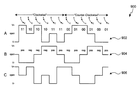
[00631 FIG. 9 is an example 900 that illustrates a polarity encoded three
phase
modulation data encoding scheme according to state diagram 800 of FIG. 8.
[00641 A 3-phase signal that rotates in two directions is transmitted using
three
conductors A, B, and C. The three signals 902, 904, and 906 (carried by
conductors
A, B, and C) that make up the 3-phase signal are independent, with each signal
being 120 degrees out of phase relative to the remaining two.
[00651 At any time, exactly two of conductors A, B, and C carry a signal, with
the
data encoding states being defined both in terms of signal flow between
conductors
and the polarity of said signal flow. Data encoding is done according to the
state
transitions as defined in state diagram 800. In one embodiment, clockwise
state
transitions (A-to-B to B-to-C, B-to-C to C-to-A, and C-to-A to A-to-B) are
used to
transmit data sequences starting with a logic 1 (10 and 11) and counter-
clockwise
state transitions (A-to-B to C-to-A, B-to-C to A-to-B, and C-to-A to B-to-C)
are used
to transmit data sequences starting with a logic zero (00 and 01).
[00661 FIG. 13 illustrates an example data recovery circuit 1300 which can be
used
to decode data transmitted according to a polarity encoded three phase
modulation
data encoding scheme. Other data recovery circuit implementation can also be
used
as would be understood by a person skilled in the art based on the teachings
herein.
The operation of recovery circuit 1300 is described below.
[00671 Recovery circuit 1300 receives input signals 1302, 1304, 1306, 1308,
1310,
and 1312 from preceding analog circuits. At any time, only one of signals
1302,
1304, 1306, 1308, 1310, and 1312 can have a value of one, depending on which
of
CA 02676079 2009-07-21
WO 2008/109478 PCT/US2008/055566
14
the encoding states just occurred. In implementation, overlaps or gaps between
the
signals may occur. Inputs signals 1302, 1304, 1306, 1308, 1310, and 1312 are
respectively coupled to the clock inputs of D flip flops 11-16. Each of D flip
flops
11-16 has its D data input coupled to a logic one, which causes its Qoutput to
have a
value of one whenever its respective clock input experiences a rising edge
transition.
For example, D flip flop 11 will have a Qoutput of one whenever input signal
1302
experiences a rising edge transition, or equivalently, whenever state A-to-B
positive
occurs. As such, D flip flops 11-16 capture which of the six states has just
occurred,
as indicated by their respective Qoutputs 1322, 1324, 1326, 1328, 1330, 1332.
Since
only one state can occur at any time, only one of outputs 1322, 1324, 1326,
1328,
1330, 1332 can continue to have a value of one at any time. As will be further
described below, there will be a short overlap whenever a new state occurs
with the
Q outputs corresponding to the current state and the new state both having a
value
of one for the duration of the delay to reset the flip-flops.
[00681 When any of the states is captured by one of D flip flops 11-16, the
other flip
flops will be reset. In circuit 1300, this is achieved using OR gates 1-6,
which
generate reset signals for respective D flip flops 11-16. OR gates 1-6 each
receives as
inputs pulses caused by rising edges on the Qoutputs of D flip flops 11-16
except for
the Qoutput of its respective D flip-flop and a Reset signal 1314. For
example, OR
gate 1 receives pulses caused by rising edges on the Q outputs 1324, 1326,
1328,
1330, and 1330 (but not Qoutput 1322 of its respective D flip flop 11) of D
flip-flops
12-16 and Reset signal 1314. Accordingly, the output of OR gate 1 will be one
whenever any state other than A-to-B positive occurs or if Reset signal 1314
is
asserted. One the other hand, when state A-to-B positive occurs and Reset
signal
1341 is not asserted, OR gate 1 will output a value of zero.
[00691 In an embodiment, to ensure that D flip-flops 11-16 are only reset
momentarily when a non-respective state occurs, the Qoutputs of D flip-flops
11-16
are coupled to OR gates 1-6 through a circuitry, which ensures that OR gates 1-
6 are
only provided with a pulse and not a continuous signal of value one. For
example, Q
CA 02676079 2009-07-21
WO 2008/109478 PCT/US2008/055566
output 1322 of D flip-flop 11 is coupled to OR gates 2-6 through an AND gate
71.
AND gate 71 receives as inputs Q output 1322 and a delayed inverted version of
Q
output 1322. Note that right before D flip-flop 11 captures an A-to-B positive
state
occurrence, the output of AND gate 71 is zero because Qoutput 1322 is zero (D
flip-
flop 11 would have been reset previously). On the other hand, the delayed
inverted
version of Q has a value of one. When the A-to-B positive input occurs, Q
output
1322 changes to one. The delayed inverted version of Qmaintains a value of one
for
the duration of the delay (generated by a delay element as illustrated) before
changing to zero. Accordingly, for the duration of the delay, AND gate 71 will
output a value of one, creating a pulse which resets flip-flops 12-16.
[0070] D flip-flops 21-26 are used to generate a double data rate clock signal
Rx_clk
1316, which transitions whenever a new input is presented. D flip-flops 21-26
respectively receive as clock inputs input signals 1302, 1304, 1306, 1308,
1310, and
1312. D flip-flops 21-26 also receive Reset signal 1314. As shown in FIG. 13,
each of
D flip flops 21-26 has its _bar output fed back to its D data input. As such,
for each
of D flip-flops 21-26, whenever its respective input clock signal experiences
a rising
edge transition, its _bar output will toggle from one to zero or from zero to
one.
The Q_bar outputs of D flip-flops 21-26 are input together through XOR gates
35
and 36, as illustrated in FIG. 13. The outputs of XOR gates 35 and 36 are, in
turn,
input together through XOR gate 37. XOR gate 37 will output a value of one
whenever an odd number of the Q_bar outputs of D flip-flops 21-26 have a value
of
one. Since only one of the _bar outputs of D flip-flops 21-26 will toggle at
any one
time while the others will maintain the same value, the output of XOR 37 will
toggle
for each change in inputs 1302, 1304, 1306, 1308, 1310, and 1312. This
generates
double data rate clock signal Rx_Clk 1316. In an embodiment, a delay element
62 is
used to ensure that Rx_Clk signal is in sync with the other signals that are
output by
data recovery circuit 1300.
[0071] OR gate 31 generates Rx_Data_Polarity signal 1318, which indicates
whether
the state that just occurred is of positive or negative polarity. OR gate 31
receives as
CA 02676079 2009-07-21
WO 2008/109478 PCT/US2008/055566
16
inputs the Q outputs 1322, 1324, and 1326 of D flip-flops 11-13, respectively.
As
such, OR gate 31 outputs a value of one whenever a positive polarity (A-to-B
positive, B-to-C positive, or C-to-A positive) input occurs. On the other
hand,
Rx_Data_Polarity signal 1318 will have a value of zero when a negative
polarity
state occurs.
[0072] OR gates 32 33, and 34 are used to capture respectively when a C-to-A
state
(positive or negative polarity), an A-to-B state (positive or negative
polarity), and a
B-to-C state (positive or negative polarity) occurs regardless of polarity.
For example
OR gate 32 receives as inputs _outputs 1326 and 1332 of D flip-flops 13 and
16,
respectively. As such, OR gate 32 outputs a value of one whenever C-to-A
positive
or C-to-A negative occurs.
[0073] The outputs of OR gates 32-34 are coupled to the D data inputs of D
flip-flops
41-46, as illustrated in FIG. 13. The output of OR gate 32 is coupled to the D
inputs
of D flip-flops 41 and 44. Similarly, the output of OR gate 33 is coupled to
the D
inputs of D flip-flops 42 and 45, and the output of OR gate 34 is coupled to
the D
inputs of D flip-flops 43 and 46. At the same time, the clock inputs of D flip-
flops
41-46 are respectively coupled to inputs 1302, 1304, 1306, 1308, 1310, and
1312.
Accordingly, for example, D flip-flop 41 will have a Qoutput of value one
whenever
the previous state is C-to-A (regardless of polarity) and the current state is
A-to-B
positive. Referring to FIG. 12, this corresponds to the clockwise transitions
into the
state A-to-B positive from either of states C-to-A positive or C-to-A
negative.
Similarly, D flip-flop 44 will have a Q output of value one whenever the
previous
state is C-to-A (regardless of polarity) and the current state is A-to-B
negative.
Referring to FIG. 12, this corresponds to the clockwise transitions into the
state A-
to-B negative from either of states C-to-A positive or C-to-A negative.
Accordingly,
D flip-flops 41-46 each captures one of the six clockwise transitions in state
diagram
1200 in FIG. 12.
[0074] The Q outputs of D flip-flops 41-46 are input together with respective
Q
outputs of D flip-flops 11-16 into respective AND gates 51-56, as illustrated
in FIG.
CA 02676079 2009-07-21
WO 2008/109478 PCT/US2008/055566
17
13. For example, the Qoutput of D flip-flop 41 is input together with the
Qoutput
1322 of D flip-flop 11 into AND gate 51. AND gates 51-56 are used to ensure
that
only one of the six clockwise transitions is reflected at any time. In other
words,
only one of the outputs of AND gates 51-56 can have a value of one at any
time. The
outputs of AND gates 51-56 are input together into an OR gate 61 to generate
Rx_Data_Phase 1320. Accordingly, Rx_Data_Phase 1320 has a value of one
whenever a clockwise phase transition occurs and a value of zero otherwise.
Note
that Rx Data Phase 1320 can have a value of zero if either a counter-clockwise
transition or a polarity-only (same phase transition; e.g., A-to-B positive to
A-to-B
negative) transition occurs. For example, if the current state is A-to-B
positive,
recovery circuit 1300 would output the same values for Rx_Data_polarity 1318
and
Rx_Data_phase 1320 if the next state is C-to-A negative or A-to-B negative.
Therefore, additional circuitry is required to distinguish between these types
of
transitions.
[0075] FIG. 14 illustrates additional circuitry 1400 for capturing polarity-
only
transitions. Inputs to circuitry 1400 include input signals 1302, 1304, 1306,
1308,
1310, and 1312 and the Q outputs 1322, 1324, 1326, 1328, 1330, and 1332 of D
flip-
flops 11-16. Circuitry 1400 includes D flip-flops 71-76, which are used to
capture
polarity-only transitions. For example, D flip-flop 71 receives input signal
1302 as
clock input and Qoutput signal 1328 as D data input and is used to capture A-
to-B
negative to A-to-B positive transitions. Note that when A-to-B negative
occurs, Q
output 1328 will have a value of one. Subsequently, when A-to-B positive
occurs, Q
output 1328 will continue to have a value of one for the duration of the delay
between the time when Qoutput 1322 changes value to one and the time when flip-
flops 12-16 are reset. During that delay duration, both input signal 1302 and
Q
output 1328 will have a value of one, causing the Q output of D flip-flop 71
to
change to a value of one. This also causes the output of AND gate 81 to have a
value
of one. The operation of D flip-flops 72-76 and respective AND gates 82-86 is
similar.
CA 02676079 2009-07-21
WO 2008/109478 PCT/US2008/055566
18
[0076] Outputs of AND gates 81-86 are input together into an OR gate 87, which
generates output signal Rx_Data_same_phase 1402. Output signal
Rx_Data_same_phase 1402 thus has a value of one whenever any one of the six
possible polarity-only state transitions occurs. As such, Rx_Data_same_phase
1402
can be used to determine whether a transition is polarity-only or counter-
clockwise,
whenever Rx_Data_phase 1320 of circuitry 1300 has a value of zero.
[0077] Note that circuitry 1400 is operable together with data recovery
circuitl300
of FIG. 13. In other words, the output Rx_Data_same_phase 1402 of circuitry
1400
is provided together with outputs Rx_Clk 1316, Rx_Data_polarity 1318, and
Rx_Data_phase 1320 of circuit 1300 to a subsequent decoder stage for decoding,
as
will be illustrated further below.
[0078] FIG. 15 is an example embodiment 1500 of a decoder 1502 that can be
used to
decode the outputs generated by the data recovery circuit illustrated in FIGs.
13 and
14. Decoder 1502 receives seven input sets 1504, 1506, 1508, 1510, 1512, 1514,
and
1516. In example embodiment 1500, each input set is a 3-bit input with one bit
for
each of the Rx_Data_phase, Rx_Data_polarity, and Rx_Data_same_phase outputs of
the data recovery circuit illustrated in FIGs. 13 and 14. Decoder 1502 decodes
the
received seven 3-bit input sets to generate a 16-bit data output 1518. Other
variations of decoder 1502 are also possible as may be understood by a person
skilled
in the art. For example, decoder 1502 may receive more or less than seven
input sets
and/or generate a different length data output 1518.
Example Serial Interface Implementations
[0079] FIGs. 10 and 11 illustrate example serial interface implementations
employing the three phase modulation data encoding schemes of the present
invention. FIG. 10 illustrates an example implementation 1000 on a printed
wiring
board. As shown, three conductors A, B, and C are interleaved with ground on
an
upper layer with a dielectric core separating them from ground in a lower
layer. In
CA 02676079 2009-07-21
WO 2008/109478 PCT/US2008/055566
19
one embodiment, the impedance from any conductor to ground has a value Z0.
FIG.
11 illustrates an example implementation 1100 using a twisted trio cable.
Three Phase Modulation for Mobile Display Digital Interface (MDDI)
[00801 The Mobile Display Digital Interface (MDDI) is a cost-effective, low
power
consumption, transfer mechanism that enables very-high-speed serial data
transfer
over a short-range communication link between a host and a client. In certain
embodiments, an MDDI interface may benefit from using the three phase
modulation data encoding schemes of the present invention.
[00811 In one aspect, an MDDI host may comprise one of several types of
devices
that can benefit from using the data encoding schemes of the present
invention. For
example, the host could be a portable computer in the form of a handheld,
laptop, or
similar mobile computing device. It could also be a Personal Data Assistant
(PDA), a
paging device, or one of many wireless telephones or modems. Alternatively,
the
host could be a portable entertainment or presentation device such as a
portable
DVD or CD player, or a game playing device. Furthermore, the host can reside
as a
host device or control element in a variety of other widely used or planned
commercial products for which a high speed communication link with a client is
desired. For example, a host could be used to transfer data at high rates from
a video
recording device to a storage based client for improved response, or to a high
resolution larger screen for presentations. In general, those skilled in the
art will
appreciate the wide variety of modern electronic devices and appliances that
may
benefit from the use of this interface, as well as the ability to retrofit
older devices
with higher data rate transport of information utilizing limited numbers of
conductors available in either newly added or existing connectors or cables.
At the
same time, an MDDI client may comprise a variety of devices useful for
presenting
information to an end user, or presenting information from a user to the host.
For
example, a micro-display incorporated in goggles or glasses, a projection
device built
CA 02676079 2012-02-21
74769-2526
into a hat or helmet, a small screen or even holographic element built into a
vehicle, such
as in a window or windshield, or various speaker, headphone, or sound systems
for
presenting high quality sound or music. Other presentation devices include
projectors or
projection devices used to present information for meetings, or for movies and
television
images. Other examples include the use of touch pads or sensitive devices,
voice
recognition input devices, security scanners, and so forth that may be called
upon to
transfer a significant amount of information from a device or system user with
little
actual "input" other than touch or sound from the user. In addition, docking
stations for
computers and car kits or desk-top kits and holders for wireless telephones
may act as
interface devices to end users or to other devices and equipment, and employ
either
clients (output or input devices such as mice) or hosts to assist in the
transfer of data,
especially where high speed networks are involved. However, those skilled in
the art will
readily recognize that the present invention is not limited to these devices,
there being
many other devices on the market, and proposed for use, that are intended to
provide end
users with high quality images and sound, either in terms of storage and
transport or in
terms of presentation at playback. The present invention is useful in
increasing the data
throughput between various elements or devices to accommodate the high data
rates
needed for realizing the desired user experience.
Conclusion
[0082] While various embodiments of the present invention have been described
above, it should be understood that they have been presented by way of example
only,
and not limitation. It will be apparent to persons skilled in the relevant art
that various
changes in form and detail can be made therein without departing from the
scope of the
claims.