Note: Descriptions are shown in the official language in which they were submitted.
CA 02687477 2009-12-07
FIELD OF THE INVENTION
The present invention generally relates to drive a display particularly light
emitting displays.
SUMMARY OF INVENTION
The disclosed technique enables integration of different peripheral circuitry
onto display
substrates using a single device.
ADVANTAGES
The new techniques can enable implementation of high output impendence current
source and
current sink based on single device architectures. Because of the reduced
circuit complexity, a
higher density integration can be achieved on the display substrate reducing
the cost of drivers.
CA 02687477 2009-12-07
This technique can be applied to different fabrication technology including
but not limited to
poly-silicon, amorphous silicon, organic semiconductor, metal oxide, and
conventional CMOS.
Also, the embodiments presented in this discloser are only examples and can be
modified by
different circuit techniques such as complimentary circuit concepts.
Most backplane technologies offer only one type of thin film transistors
(TFT), either p-type or
n-type. Thus, the device-type limitation needs to be overcome by some circuit
technique in order
to enable integration of more useful circuitry onto the display substrate
which can lead to better
performance and lower cost. The main circuit blocks for driving active matrix
organic light
emitting diodes are current sources (or sinks) and voltage to current
convertors.
For example, p-type devices have been used in conventional current mirror and
current sources
since the source terminal of at least one TFT is fixed (e.g. VDD). The current
output is coming
through the drain and so change in the output line will only affect the drain
voltage. As a result,
the output current will stay constant despite change in the line voltage
(leading to high output
resistance current sources). On the other hand, if a p-type TFT is used for
current sink, the source
of the TFT will be connected to the output line. Thus, any change in the
output voltage due to
variation in the output load, we affect the gate-source voltage directly.
Consequently, the output
current will not be constant for different loads. To overcome this issue, a
circuit design technique
is needed to control the effect of source voltage variability on the output
current.
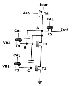
Figure 1 shows an embodiment of a current sink using only p-type devices.
During the
calibration cycle, CAL is low and so T2, T4 and T5 are ON while T6 is OFF. As
a result, the
current adjusts the voltage at node A to allow all the current to pass through
Ti and T3. After
calibration, CAL is high and ACS is low; thus, T6 is ON and a negative
polarity current is
applied through T6. Here, the storage capacitor along with the source
degenerate effect (between
Ti and T3) preserves the copied current, thus providing very high output
impedance. The signal
diagram of the current sink operation is shown in Fig. 2.
Figure 3 shows the simulation result for the output current of the current
sink presented in Fig. 1
as function of output voltage. Despite using p-type device, the output current
is significantly
stable despite the change in the output voltage.
Also, the output current is highly uniform despite the high level of non-
uniformity in the
backplanes (normally caused by process-induced effects). Figure 4 shows a
parameter variation
in a typical poly-Si process which is used for the simulation and analysis
results. Figure 5
highlights the Mont Carlo simulation results. Here, over 12% variation in
mobility and 30%
variation in the threshold voltage (VT) is considered, however, the output
current variation is less
than I%.
Figure 6 shows another embodiment of the current source. The operation of this
circuit is the
same as the one shown in Fig. 1.
The circuit shown in Figure 1 and 5 can be used to develop more complex
circuit and system
blocks. Figure 7 shows the use of this circuit in a voltage to current
convertor. During the
calibration, CAL is low and a VB4 is applied to node B. Here, the current of
TI-T3-T5 branch is
CA 02687477 2009-12-07
adjusted to allow VB4 at node B (see Fig. 8). As a result, a current
correlated to VB3 and VB4
will pass through lout.
CA 02687477 2009-12-07
Fig 1 shows a current sink embodiment using p-type TFTs.
Fig 2 shows the signal diagram for driving the circuit shown in Fig. 1.
Fig 3 displays the output current of the circuit in Fig. I versus the output
voltage.
Fig 4 demonstrates parameter variation used in a typical poly-Si process.
Fig 5 highlights the output current uniformity of the circuit demonstrated in
Fig 1.
Fig 6 shows another embodiment of the current sink using p-type TFTs.
Fig 7 shows a voltage-to-current convertor based on the circuit shown in Fig.
1.
Fig 8 shows the signal diagram for driving the circuit in Fig. 7.