Note: Descriptions are shown in the official language in which they were submitted.
CA 02692542 2010-01-04
S08P1066
1/39
DISPLAY DEVICE, METHOD FOR CORRECTING UNEVEN LIGHT EMISSION
AND COMPUTER PROGRAM
TECHNICAL FIELD
[0001]
The present invention relates to a display device, a method for correcting
uneven
light emission, and a computer program, and more particularly, to an active
matrix type
display device that is configured such that scanning lines for selecting
pixels in a
predetermined scan cycle, data lines that provide luminance information for
driving the
pixels, and pixel circuits for controlling an amount of electric current based
on the
luminance information and causing light emitting elements to emit light
according to the
amount of electric current are arranged in a matrix configuration, as well as
a drive
method for the display device.
BACKGROUND ART
[0002]
Liquid crystal display devices that use liquid crystals and plasma display
devices that use plasma have found practical application as flat and thin
display devices.
[0003]
A liquid crystal display device provides a backlight, and displays images by
altering an array of liquid crystal molecules by application of voltage,
passing or
blocking light from the backlight. Additionally, a plasma display device
causes a
plasma state to occur by application of voltage to a gas that is enclosed
within a panel,
and ultraviolet light produced by energy occurring on return from the plasma
state to the
original state becomes visible light through irradiation of a fluorescent
body, displaying
an image.
[0004]
Meanwhile, in recent years, development has been progressing for self-
illuminating type displays employing organic electroluminescent (EL) elements
in which
the element itself emits light when voltage is applied. When the organic EL
element
receives energy by electrolysis, it changes from a base state to an excited
state, and at
the time of return from the excited state to the base state, the difference in
energy is
emitted as light. The organic EL display device is a display device that
displays images
using these organic EL elements.
[0005]
A self-illuminating type display device, unlike a liquid crystal display
device,
which requires a backlight, requires no backlight because the elements
themselves emit
light, and thus it is possible to make the structure thin compared to a liquid
crystal
display device. Additionally, because motion characteristics, viewing angle
characteristics, color reproduction performance, and the like are superior to
a liquid
crystal display device, self-illuminating type display devices using organic
EL elements
are attracting attention as next-generation flat and thin display devices.
DISCLOSURE OF THE INVENTION
Problem to be Solved by the Invention
[0006]
A manufacturing process of such a self-illuminating type display device
includes
CA 02692542 2010-01-04
S08P1066
2/39
a process in which thin film transistors (TFTs) that form pixels are exposed
to a laser
beam. In this exposure process, a single laser beam is spread out in a fan
shape by
optical means, and the fan-shaped laser beam is used to perform the exposure
process of
TFTs that are arranged in the vertical direction of a panel that displays
images. Then,
by moving the panel in the horizontal direction, the exposure process is
performed on
the TFTs that are arranged on the entire panel.
[0007]
However, because the laser beam is spread out in a fan shape, in some cases,
the
laser beam is not irradiated evenly to the panel. As a result, stripe-like
uneven light
emission is likely to occur in the horizontal direction and the vertical
direction of the
manufactured panel. Further, in some cases, uneven light emission occurs
locally, as
well as in the horizontal direction and the vertical direction.
[0008]
Accordingly, the present invention addresses the problems described above, and
it is an object of the present invention to provide a display device, a method
for
correcting uneven light emission and a computer program that are new and
improved and
that are capable of effectively correcting uneven light emission that occurs
as stripes in
the horizontal direction and the vertical direction, and uneven light emission
that occurs
locally, and capable of displaying images while suppressing uneven light
emission.
Means for Solving the Problem
[0009]
In order to solve the problems that are described above, according to an
aspect
of the present invention, there is provided a display device that includes a
display unit in
which a pixel, a scanning line and a data line are arranged in the form of a
matrix, the
pixel having a light emitting element that emits light in accordance with an
amount of an
electric current and a pixel circuit that controls, in accordance with a video
signal, an
electric current applied to the light emitting element, the scanning line
supplying to the
pixel, in a predetermined scan cycle, a selection signal that selects the
pixel that will
emit light, and the data line supplying the video signal to the pixel. The
display device
is characterized by including: an unevenness correction information storage
unit that
stores unevenness correction information used to correct uneven light emission
of the
display unit; and an unevenness correction unit that corrects uneven light
emission of the
display unit by reading out the unevenness correction information from the
unevenness
correction information storage unit and by performing signal processing on the
video
signal having a linear characteristic. The unevenness correction unit corrects
the
uneven light emission by using a first correction that is applied to a section
in which
uneven light emission is occurring in a horizontal direction or a vertical
direction of the
display unit, and/or a second correction that is applied to a section of the
display unit in
which uneven light emission is occurring.
[0010]
With the structure described above, the unevenness correction information
storage unit stores unevenness correction information used to correct uneven
light
emission of the display unit, and the unevenness correction unit corrects
uneven light
emission of the display unit by reading out the unevenness correction
information from
the unevenness correction information storage unit and by performing signal
processing
on the video signal having a linear characteristic. The unevenness correction
unit
corrects the uneven light emission by using the first correction that is
applied to a
section in which uneven light emission is occurring in the horizontal
direction or the
CA 02692542 2010-01-04
S08P1066
3/39
vertical direction of the display unit, and/or the second correction that is
applied to a
section of the display unit in which uneven light emission is occurring. As a
result, it
is possible to effectively correct uneven light emission that occurs as
stripes in the
horizontal direction and the vertical direction and uneven light emission that
occurs
locally.
[0011]
Further, in order to solve the problems that are described above, according to
another aspect of the present invention, there is provided a method for
correcting uneven
light emission of a display device that includes a display unit in which a
pixel, a
scanning line and a data line are arranged in the form of a matrix, the pixel
having a
light emitting element that emits light in accordance with an amount of an
electric
current and a pixel circuit that controls, in accordance with a video signal,
an electric
current applied to the light emitting element, the scanning line supplying to
the pixel, in
a predetermined scan cycle, a selection signal that selects the pixel that
will emit light,
and the data line supplying the video signal to the pixel. The method for
correcting
uneven light emission is characterized by including the steps of: storing
unevenness
correction information used to correct uneven light emission of the display
unit; and
correcting unevenness by reading out the unevenness correction information
stored in
the unevenness correction information storing step and by performing signal
processing
on the video signal having a linear characteristic. The unevenness correction
step
corrects the uneven light emission by using a first correction that is applied
to a section
in which uneven light emission is occurring in a horizontal direction or a
vertical
direction of the display unit, and/or a second correction that is applied to a
section of the
display unit in which uneven light emission is occurring.
[0012]
Further, in order to solve the problems that are described above, according to
another aspect of the present invention, there is provided a computer program
that
causes a computer to execute control of a display device that includes a
display unit in
which a pixel, a scanning line and a data line are arranged in the form of a
matrix, the
pixel having a light emitting element that emits light in accordance with an
amount of an
electric current and a pixel circuit that controls, in accordance with a video
signal, an
electric current applied to the light emitting element, the scanning line
supplying to the
pixel, in a predetermined scan cycle, a selection signal that selects the
pixel that will
emit light, and the data line supplying the video signal to the pixel. The
computer
program is characterized by including the step of correcting unevenness by
performing
signal processing on the video signal having a linear characteristic, based on
unevenness
correction information that is used to correct uneven light emission of the
display device
and that is stored in advance. The unevenness correction step corrects the
uneven light
emission by using a first correction that is applied to a section in which
uneven light
emission is occurring in a horizontal direction or a vertical direction of the
display unit,
and/or a second correction that is applied to a section of the display unit in
which
uneven light emission is occurring.
Effects of the Invention
[0013]
As described above, according to the present invention, a display device, a
method for correcting uneven light emission and a computer program can be
provided
that are new and improved and that are capable of effectively correcting
uneven light
emission that occurs as stripes in the horizontal direction and the vertical
direction, and
CA 02692542 2010-01-04
S08P1066
4/39
uneven light emission that occurs locally, and capable of displaying images
while
suppressing uneven light emission.
BRIEF DESCRIPTION OF THE DRAWINGS
[0014]
FIG. 1 is an explanatory diagram that explains the structure of a display
device
100 according to an embodiment of the present invention.
FIG. 2A is an explanatory diagram that explains, in the form of a graph, a
transition in a characteristic of a signal that flows in the display device
100 according to
the embodiment of the present invention.
FIG. 2B is an explanatory diagram that explains, in the form of a graph, a
transition in a characteristic of the signal that flows in the display device
100 according
to the embodiment of the present invention.
FIG. 2C is an explanatory diagram that explains, in the form of a graph, a
transition in a characteristic of the signal that flows in the display device
100 according
to the embodiment of the present invention.
FIG. 2D is an explanatory diagram that explains, in the form of a graph, a
transition in a characteristic of the signal that flows in the display device
100 according
to the embodiment of the present invention.
FIG. 2E is an explanatory diagram that explains, in the form of a graph, a
transition in a characteristic of the signal that flows in the display device
100 according
to the embodiment of the present invention.
FIG. 2F is an explanatory diagram that explains, in the form of a graph, a
transition in a characteristic of the signal that flows in the display device
100 according
to the embodiment of the present invention.
FIG. 3 is a sectional view that shows an example of cross-sectional structure
of a
pixel circuit that is provided in a panel 158.
FIG. 4 is an equivalent circuit diagram of a 5Tr/IC drive circuit.
FIG. 5 is a timing chart of drive of the 5Tr/IC drive circuit.
FIG 6A is an explanatory figure that shows an on/off state and the like of
each
transistor in the 5Tr/1C drive circuit.
FIG. 6B is an explanatory figure that shows the on/off state and the like of
each
of the transistors in the 5Tr/1C drive circuit.
FIG. 6C is an explanatory figure that shows the on/off state and the like of
each
of the transistors in the 5Tr/1C drive circuit.
FIG. 6D is an explanatory figure that shows the on/off state and the like of
each
of the transistors in the 5Tr/1C drive circuit.
FIG. 6E is an explanatory figure that shows the on/off state and the like of
each
of the transistors in the 5Tr/1C drive circuit.
FIG. 6F is an explanatory figure that shows the on/off state and the like of
each
of the transistors in the 5Tr/1C drive circuit.
FIG. 6G is an explanatory figure that shows the on/off state and the like of
each
of the transistors in the 5Tr/1C drive circuit.
FIG. 6H is an explanatory figure that shows the on/off state and the like of
each
of the transistors in the 5Tr/1C drive circuit.
FIG. 61 is an explanatory figure that shows the on/off state and the like of
each
of the transistors in the 5Tr/IC drive circuit.
FIG. 7 is an equivalent circuit diagram of a 2Tr/1C drive circuit.
CA 02692542 2010-01-04
S08P1066
5/39
FIG. 8 is a timing chart of drive of the 2Tr/1 C drive circuit.
FIG. 9A is an explanatory figure that shows an on/off state and the like of
each
transistor in the 2Tr/1C drive circuit.
FIG. 9B is an explanatory figure that shows the on/off state and the like of
each
of the transistors in the 2Tr/1C drive circuit.
FIG. 9C is an explanatory figure that shows the on/off state and the like of
each
of the transistors in the 2Tr/1C drive circuit.
FIG. 9D is an explanatory figure that shows the on/off state and the like of
each
of the transistors in the 2Tr/1C drive circuit.
FIG. 9E is an explanatory figure that shows the on/off state and the like of
each
of the transistors in the 2Tr/1C drive circuit.
FIG. 9F is an explanatory figure that shows the on/off state and the like of
each
of the transistors in the 2Tr/1C drive circuit.
FIG. 10 is an equivalent circuit diagram of a 4Tr/1C drive circuit.
FIG. 11 is an equivalent circuit diagram of a 3Tr/1C drive circuit.
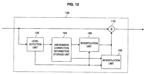
FIG. 12 is an explanatory figure that explains the configuration of an
unevenness
correction unit 130 according to the embodiment of the present invention.
FIG. 13 is an explanatory figure that explains a concept of a method for
correcting uneven light emission in the display device 100.
FIG. 14A is an explanatory figure that shows known grid type correction that
takes the entire screen as a processing region.
FIG. 14B is an explanatory figure that shows that the processing region is
limited to just a particular region in which uneven light emission is
occurring, and spot
correction is performed.
FIG. 15 is an explanatory figure that explains, in the form of a graph, about
correction of uneven light emission by the method for correcting uneven light
emission
in the display device 100 according to the embodiment of the present
invention.
FIG. 16 is an explanatory figure that explains a case in which uneven light
emission that is locally occurring on the panel 158 is corrected by the spot
correction.
FIG. 17 is an explanatory figure that explains the configuration of an
unevenness
correction unit 130'.
FIG. 18A is an explanatory figure that shows the manner in which unevenness
correction is performed in a case where the unevenness correction is also
performed on a
low gradation side.
FIG. 18B is an explanatory figure that shows the manner in which unevenness
correction is performed in a case where the unevenness correction is not
performed on a
low gradation side.
DESCRIPTION OF REFERENCE NUMERALS
[0015]
100 display device
104 control unit
106 recording unit
110 signal processing integrated circuit
112 edge blurring unit
114 I/F unit
116 linear conversion unit
118 pattern generation unit
CA 02692542 2010-01-04
S08P1066
6/39
120 color temperature adjustment unit
122 still image detection unit
124 long-term color temperature correction unit
126 light emission time control unit
128 signal level correction unit
130 unevenness correction unit
132 gamma conversion unit
134 dither processing unit
136 signal output unit
138 long-term color temperature correction detection unit
140 gate pulse output unit
142 gamma circuit control unit
150 storage unit
152 data driver
154 gamma circuit
156 overcurrent detection unit
158 panel
162 level detection unit
164 unevenness correction information storage unit
166, 168 interpolation unit
170 adder
BEST MODE FOR CARRYING OUT THE INVENTION
[0016]
Hereinafter, preferred embodiments of the present invention will be described
in
detail with reference to the appended drawings. Note that, in this
specification and the
appended drawings, structural elements that have substantially the same
function and
structure are denoted with the same reference numerals, and repeated
explanation of
these structural elements is omitted.
[0017]
First, a structure of a display device according to an embodiment of the
present
invention is described. FIG. 1 is an explanatory diagram that explains the
structure of a
display device 100 according to the embodiment of the present invention. The
structure of the display device 100 according to the embodiment of the present
invention
is described below with reference to FIG. 1.
[0018]
As shown in FIG. 1, the display device 100 according to the embodiment of the
present invention includes a control unit 104, a recording unit 106, a signal
processing
integrated circuit 110, a storage unit 150, a data driver 152, a gamma circuit
154, an
overcurrent detection unit 156, and a panel 158.
[0019]
The signal processing integrated circuit 110 includes an edge blurring unit
112,
an I/F unit 114, a linear conversion unit 116, a pattern generation unit 118,
a color
temperature adjustment unit 120, a still image detection unit 122, a long-term
color
temperature correction unit 124, a light emission time control unit 126, a
signal level
correction unit 128, an unevenness correction unit 130, a gamma conversion
unit 132, a
dither processing unit 134, a signal output unit 136, a long-term color
temperature
correction detection unit 138, a gate pulse output unit 140, and a gamma
circuit control
CA 02692542 2010-01-04
S08P1066
7/39
unit 142.
[0020]
When receiving a video signal, the display device 100 analyzes the video
signal,
and turns on pixels arranged in the panel 158, mentioned later, according to
the analyzed
contents, so as to display a video through the panel 158.
[0021]
The control unit 104 controls the signal processing integrated circuit 110 and
sends and receives signals to and from the I/F unit 114. Additionally, the
control unit
104 executes various signal processing on the signals received from the I/F
unit 114.
The signal processing executed in the control unit 104 includes, for example,
calculation
of gain to be used for adjusting luminance of an image displayed on the panel
158.
[0022]
The recording unit 106 is for storing information for controlling the signal
processing integrated circuit 110 in the control unit 104 therein. A memory
that can
store information without deletion of the information even if power of the
display device
100 is turned off is preferably used as the recording unit 106. An EEPROM
(Electronically Erasable and Programmable Read Only Memory) that can rewrite
contents electronically is desirably used as the memory that is adopted as the
recording
unit 106. The EEPROM is a nonvolatile memory which can write or delete data
with
the EEPROM being packaged on a substrate, and is suitable for storing
information of
the display device 100 that changes moment by moment.
[0023]
The signal processing integrated circuit 110 inputs a video signal and
executes
signal processing with respect to the input video signal. In the present
embodiment, the
video signal input into the signal processing integrated circuit 110 is a
digital signal, and
signal width is 10 bits. The signal processing to be executed on the input
video signal
is executed in the respective sections in the signal processing integrated
circuit 110.
[0024]
The edge blurring unit 112 executes signal processing for blurring an edge on
the input video signal. Specifically, the edge blurring unit 112 intentionally
shifts an
image and blurs its edge so as to prevent a phenomenon of burn-in of the image
onto the
panel 158.
[0025]
The linear conversion unit 116 executes signal processing for converting a
video
signal whose output with respect to an input has a gamma characteristic into a
video
signal having a linear characteristic. When the linear conversion unit 116
executes the
signal processing so that the output with respect to the input has the linear
characteristic,
various processing with respect to images displayed on the panel 158 becomes
easy.
The signal processing in the linear conversion unit 116 widens the signal
width of the
video signal from 10 bits to 14 bits. Once the video signal has been converted
by the
linear conversion unit 116 such that it has the linear characteristic, it is
converted in the
gamma conversion unit 132, which is described later, such that it has the
gamma
characteristic.
[0026]
The pattern generation unit 118 generates test patterns to be used in the
image
processing inside the display device 100. The test patterns to be used in the
image
processing in the display device 100 include, for example, a test pattern
which is used
for display inspection of the panel 158.
CA 02692542 2010-01-04
S08P1066
8/39
[0027]
The color temperature adjustment unit 120 adjusts color temperature of images,
and adjusts colors to be displayed on the panel 158 of the display device 100.
Although not shown in FIG. 1, the display device 100 includes color
temperature
adjusting section which adjusts color temperature, and when a user operates
the color
temperature adjusting section, color temperature of images to be displayed on
the screen
can be adjusted manually.
[0028]
The long-term color temperature correction unit 124 corrects deterioration
with
age due to variation in luminance/time characteristic (LT characteristic) of
respective
colors R (red), G (green), and B (blue) of organic EL elements. Because the
organic EL
elements have different LT characteristics of R, G, and B, color balance
deteriorates over
light emission time. The long-term color temperature correction unit 124
corrects the
color balance.
[0029]
The light emission time control unit 126 calculates a duty ratio of a pulse at
the
time of displaying an image on the panel 158, and controls the light emission
time of the
organic EL elements. The display device 100 applies an electric current to the
organic
EL elements in the panel 158 while the pulse is in a HI state, so as to cause
the organic
EL elements to emit light and display an image.
[0030]
The signal level correction unit 128 corrects the level of the video signal
and
adjusts the luminance of the video to be displayed on the panel 158 in order
to prevent
an image burn-in phenomenon. In the image burn-in phenomenon, deterioration of
light emission characteristics occurs in a case where the light emission
frequency of a
specific pixel is high compared to other pixels, leading to a decline in
luminance of the
pixel that has deteriorated compared with other pixels which have not
deteriorated, and
the difference in luminance with the surrounding portion which has not
deteriorated
becomes larger. Due to this difference in luminance, text appears to be burned
into the
screen.
[00311
The signal level correction unit 128 calculates the amount of light emission
of
respective pixels or a pixel group based on the video signal and the duty
ratio of the
pulse calculated by the light emission time control unit 126, and calculates
gain for
reducing the luminance according to need based on the calculated amount of
luminance,
so as to multiply the video signal by the calculated gain.
[0032]
The long-term color temperature correction detection unit 138 detects
information for correction in the long-term color temperature correction unit
124. The
information detected by the long-term color temperature correction detection
unit 138 is
sent to the control unit 104 via the I/F unit 114, and is recorded in the
recording unit 106
via the control unit 104.
[0033]
The unevenness correction unit 130 corrects unevenness of images and videos
displayed on the panel 158. In the unevenness correction unit 130, horizontal
stripes
and vertical stripes of the panel 158 and uneven light emission that occurs in
localized
areas of the screen are corrected based on the level of an input signal and a
coordinate
position.
CA 02692542 2010-01-04
S08P1066
9/39
[0034]
The gamma conversion unit 132 executes signal processing for converting the
video signal converted into a signal having a linear characteristic by the
linear
conversion unit 116 into a signal having a gamma characteristic. The signal
processing
executed in the gamma conversion unit 132 is signal processing for canceling
the gamma
characteristic of the panel 158 and converting a signal into a signal having a
linear
characteristic so that the organic EL elements in the panel 158 emit light
according to
the electric current of the signal. When the gamma conversion unit 132
performs the
signal processing, the signal width changes from 14 bits to 12 bits.
[0035]
The dither processing unit 134 executes dithering with respect to the signal
converted by the gamma conversion unit 132. The dithering provides display
where
displayable colors are combined in order to express medium colors in an
environment in
which the number of usable colors is small. By executing dithering by the
dither
processing unit 134, colors which intrinsically cannot be displayed on the
panel can be
simulated and expressed. The signal width is changed from 12 bits to 10 bits
by the
dithering in the dither processing unit 134.
[0036]
The signal output unit 136 outputs the signal after dithering by the dither
processing unit 134 to the data driver 152. The signal sent from the signal
output unit
136 to the data driver 152 is a signal multiplied by information about the
amount of light
emission of respective colors R, G, and B, and the signal multiplied by the
information
about the light emission time is output in the form of a pulse from the gate
pulse output
unit 140.
[0037]
The gate pulse output unit 140 outputs a pulse for controlling the light
emission
time of the panel 158. The pulse output from the gate pulse output unit 140 is
a pulse
calculated by the light emission time control unit 126 based on the duty
ratio. The
pulse from the gate pulse output unit 140 determines the light emission time
of each
pixel on the panel 158.
[0038]
The gamma circuit control unit 142 gives a setting value to the gamma circuit
154. The setting value that is given by the gamma circuit control unit 142 is
a
reference voltage to be given to ladder resistance of a D/A converter
contained inside the
data driver 152.
[0039]
The storage unit 150 stores, in association with one another, information on
one
of a pixel and a group of pixels that emits light that exceeds a specified
luminance and
information on an amount by which the specified luminance is exceeded. The two
types of information become necessary when a luminance is corrected in the
signal level
correction unit 128. Unlike the recording unit 106, a memory in which contents
are
deleted when the power is turned off may be used as the storage unit 150, and,
for
example, SDRAM (Synchronous Dynamic Random Access Memory) is desirably used as
such a memory.
[0040]
In a case where an overcurrent is produced by substrate short circuit or the
like,
the overcurrent detection unit 156 detects the overcurrent and notifies the
gate pulse
output unit 140. In a case where an overcurrent is produced, the overcurrent
detection
CA 02692542 2010-01-04
S08P1066
10/39
and notification by the overcurrent detection unit 156 can prevent the
overcurrent from
being applied to the panel 158.
[0041]
The data driver 152 executes signal processing with respect to the signal
received from the signal output unit 136, and outputs a signal for displaying
video on the
panel 158 to the panel 158. The data driver 152 includes a D/A converter that
is not
shown in the drawings, and the D/A converter converts a digital signal into an
analog
signal and outputs the analog signal.
[0042]
The gamma circuit 154 gives a reference voltage to the ladder resistance of
the
D/A converter contained inside the data driver 152. The reference voltage to
be given
to the ladder resistance is generated by the gamma circuit control unit 142.
[0043]
The panel 158 accepts as inputs an output signal from the data driver 152 and
an
output pulse from the gate pulse output unit 140, causing the organic EL
elements, which
are examples of self-illuminating type elements, to emit light to display
moving images
and still images according to the signal and the pulse that are input. In the
panel 158,
the shape of the surface that displays the images is a plane. The organic EL
elements
are self-illuminating type elements which emit light when a voltage is
applied, and their
amount of light emission is proportional to the voltage. Consequently, an IL
characteristic (current/light emission amount characteristic) of the organic
EL elements
also comes to have a proportional relationship.
[0044]
In the panel 158, not shown in the figure, scanning lines that select pixels
in a
predetermined scanning cycle, data lines that give luminance information for
driving the
pixels, and pixel circuits that control the amount of electric current based
on the
luminance information and cause the organic EL elements as light emitting
elements to
emit light according to the amount of electric current, are structured by
arrangement in a
matrix pattern. As the scanning lines, the data lines and the pixel circuits
are
configured in this way, the display device 100 can display video images in
accordance
with the video signals.
[0045]
The structure of the display device 100 according to the embodiment of the
present invention has been described above with reference to FIG 1. The
display
device 100 according to the embodiment of the present invention depicted in
FIG. 1
converts a video signal to a signal having a linear characteristic using the
linear
conversion unit 116 and thereafter inputs the converted video signal into the
pattern
generation unit 118, but the pattern generation unit 118 and the linear
conversion unit
116 may be interchanged.
[0046)
Next, a characteristic transition of a signal flowing in the display device
100
according to the embodiment of the present invention is described below. FIGS.
2A
through 2F are explanatory diagrams that explain, in the form of graphs,
transitions in
characteristics of the signal that flows in the display device 100 according
to the
embodiment of the present invention. In the respective graphs in FIGS. 2A to
2F, the
horizontal axis represents input and the vertical axis represents output.
[0047]
FIG. 2A illustrates that when a subject is input, the linear conversion unit
116
CA 02692542 2010-01-04
S08P1066
11/39
multiplies a video signal whose output A with respect to the light quantity of
the subject
has a gamma characteristic by an inverse gamma curve (linear gamma) so as to
convert
the video signal into a video signal whose output with respect to the light
quantity of the
subject has a linear characteristic.
[0048]
FIG. 2B illustrates that the gamma conversion unit 132 multiplies a video
signal
converted so that an output B with respect to the input of the light quantity
of the subject
has a linear characteristic by a gamma curve, so as to convert the video
signal into a
video signal whose output with respect to the input of the light quantity of
the subject
has a gamma characteristic.
[0049]
FIG. 2C illustrates that the data driver 152 performs D/A conversion of a
video
signal, which is converted so that an output C with respect to the input of
the light
quantity of the subject has the gamma characteristic, into an analog signal.
In the D/A
conversion, a relationship between input and output has the linear
characteristic.
Consequently, the data driver 152 performs D/A conversion on a video signal,
and when
the light quantity of the subject is input, an output voltage has the gamma
characteristic.
[0050]
FIG. 2D illustrates that when the video signal which was subject to the D/A
conversion is input into a transistor included in the panel 158, both gamma
characteristics are canceled. The VI characteristic of the transistor is the
gamma
characteristic which has a curve inverse to a gamma characteristic of the
output voltage
with respect to the input of the light quantity of the subject. Consequently,
when the
light quantity of the subject is input, the conversion can be again carried
out so that the
output current has a linear characteristic.
[0051]
FIG. 2E illustrates that when the light quantity of the subject is input, the
signal
whose output current has a linear characteristic is input into the panel 158,
and the
signal having the linear characteristic is multiplied by the IL characteristic
of the organic
EL elements having the linear characteristic.
[0052]
As a result, as shown in FIG. 2F, when the light quantity of the subject is
input,
the amount of light emission of the panel (OLED; Organic Light Emitting Diode)
has the
linear characteristic, and thus by converting the video signal in the linear
conversion
unit 116 so as to have a linear characteristic, it becomes possible to perform
signal
processing on the interval to the gamma conversion unit 132 from the linear
conversion
unit 116 in the signal processing integrated circuit 110 shown in FIG. 1 as a
linear region.
[0053]
The characteristic transitions of the signals flowing in the display device
100
according to the embodiment of the present invention have been described
above.
[0054]
Pixel circuit structure
Next, one example of the structure of the pixel circuit disposed in the panel
158
that is shown in FIG. 1 will be described.
[0055]
FIG. 3 is a cross-sectional view depicting one example of cross-sectional
structure of the pixel circuit disposed in the panel 158 that is shown in FIG.
1. As
shown in FIG. 3, the pixel circuit disposed in the panel 158 has a structure
in which an
CA 02692542 2010-01-04
S08P1066
12/39
insulation film 1202, an insulation leveling film 1203, and a window
insulation film
1204 are formed in that order on a glass substrate 1201 in which is formed a
drive circuit
including a drive transistor 1022 and the like, and an organic EL element 1021
is
disposed in a concavity 1204A in the window insulation film 1204. Here, of the
respective structural elements of the drive circuit, only the drive transistor
1022 is
depicted, and indication of other structural elements is omitted.
[0056]
The organic EL element 1021 is made up of an anode electrode 1205 composed
of metal or the like formed on a bottom portion of the concavity 1204A in the
window
insulation film 1205, an organic layer (electron transport layer, light
emission layer, and
hole transport layer/hole implantation layer) 1206 formed on the anode
electrode 1206,
and a cathode electrode 1207 made up of a transparent conductive film or the
like
formed commonly on all pixels on the organic layer 1206.
[0057]
In this organic EL element 1021, the organic layer 1206 is formed by
sequentially depositing a hole transport layer/hole implantation layer 2061, a
light
emission layer 2062, an electron transport layer 2063, and an electron
implantation layer
(not illustrated) on the anode electrode 1205. Accordingly, light is emitted
when
electrons and holes in the light emission layer 2062 in the organic layer 1206
electron
hole recombine due to current flowing from the drive transistor 1022 via the
anode
electrode 1205 to the organic layer 1206, under current drive by the drive
transistor 1022.
[0058]
The drive transistor 1022 is made up of a gate electrode 1221, a source/drain
region 1223 disposed on one side of a semiconductor layer 1222, a drain/source
region
1224 disposed on the other side of the semiconductor layer 1222, and a channel
forming
region 1225 of a portion facing the gate electrode 1221 of the semiconductor
layer 1222.
The source/drain region 1223 is electrically connected to the anode electrode
1205 of the
organic EL element 1021 via a contact hole.
[0059]
Accordingly, as shown in FIG. 3, after the organic EL element 1021 has been
formed in pixel units, via the insulation film 1202, the insulation leveling
film 1203, and
the window insulation film 1204, on the glass substrate 1201 in which is
formed the
drive circuit including the drive transistor 1022, a sealing substrate 1209 is
attached by
an adhesive 1210 via a passivation film 1208, and the organic EL element 1021
is sealed
by the sealing substrate 1209, forming the panel 158.
[0060]
Drive circuit
Next, one example of the structure of the drive circuit disposed in the panel
158
that is shown in FIG. 1 will be described.
[00611
Various circuits that are shown in FIG. 4 and the like exist as drive circuits
for
driving a light emission unit ELP provided with organic EL elements, but items
common
to a drive circuit fundamentally made up of five transistors/one capacitor
(which
hereinafter may in some cases be called a 5Tr/1C drive circuit), a drive
circuit
fundamentally made up of four transistors/one capacitor (which hereinafter may
in some
cases be called a 4Tr/IC drive circuit), a drive circuit fundamentally made up
of three
transistors/one capacitor (which hereinafter may in some cases be called a
3Tr/1C drive
circuit), and a drive circuit fundamentally made up of two transistors/one
capacitor
CA 02692542 2010-01-04
S08P1066
13/39
(which hereinafter may in some cases be called a 2Tr/1C drive circuit) will
firstly be
explained below.
[0062]
For convenience, each transistor constituting a drive circuit is, in
principle,
described as being made up of an n-channel type thin film transistor (TFT).
Note,
however, that depending on the case, a portion of the transistors can also be
made up of
p-channel type TFTs. Note that a structure in which transistors are formed on
a
semiconductor substrate or the like can also be used. The structure of the
transistors
constituting the drive circuit is not particularly limited. In the explanation
below,
transistors constituting drive circuits are described as being of enhancement
type, but are
not limited to this. Depression type transistors may be used. Additionally,
transistors
constituting a drive circuit may be of single-gate type, or may be of dual-
gate type.
[0063]
In the explanation below, a display device is made up of (N / 3) x M pixels
arranged in a two-dimensional matrix pattern, and one pixel is taken to be
made up of
three sub-pixels (a red light emitting sub-pixel that emits red light, a green
light emitting
sub-pixel that emits green light, and a blue light emitting sub-pixel that
emits blue light).
Additionally, the light emitting elements constituting each pixel are taken to
be driven in
line sequence, and a display frame rate is taken to be FR (times/second). That
is to say,
(N / 3) pixels arranged in an mth column (where m= 1, 2, 3,..., M), or more
specifically,
light emitting elements respectively made up of N sub-pixels, are driven
simultaneously.
To state this differently, in respective light emitting elements constituting
one column,
timing of their light emission/light nonemission is controlled by the unit of
the column
to which they belong. Note that processing for writing a video signal with
regard to
respective pixels making up one column may be processing to write a video
signal for all
pixels simultaneously (which hereinafter may in some cases be called simply
simultaneous write processing), or may be processing to write a sequential
video signal
for each respective pixel (which hereinafter may in some cases be called
simply
sequential write processing). Which write processing is used may be suitable
selected
according to the structure of the drive circuit.
[0064]
Here, in principle, drive and operation relating to a light emitting element
posited at an mth column and nth row (where n = 1, 2, 3,..., N) are described,
but such a
light emitting element refers, hereinafter, to an (n, m)th light emitting
element or (n,
m)th sub-pixels. Accordingly, various processing (threshold voltage cancel
processing,
write processing, and mobility correction processing, described later) is
performed until
a horizontal scanning period of respective pixels arranged in the mth column
(mth
horizontal scanning period) ends. Note that performing write processing and
mobility
correction processing within the mth horizontal scanning period is necessary.
On the
other hand, depending on the type of the drive circuit, threshold voltage
cancel
processing and preprocessing accompanying this can be performed in advance of
the mth
horizontal scanning period.
[0065]
Accordingly, after the various processing described above has finished
completely, light emission units constituting the respective light emitting
elements
arranged in the mth column are caused to emit light. Note that after the
various
processing described above has finished completely, the light emission units
may be
caused to emit light immediately, or the light emission units may be caused to
emit light
CA 02692542 2010-01-04
S08P1066
14/39
after a predetermined period (for example, a predetermined horizontal scanning
period
for several columns) has elapsed. This predetermined period can be set
suitably
according to a specification of the display device or structure or the like of
the drive
circuit. Note that in the explanation below, for convenience of explanation,
the light
emission unit is taken to be caused to emit light immediately after the
various types of
processing finish. Accordingly, light emission of the light emission units
constituting
the respective light emitting elements arranged in the mth column is continued
until just
before the start of a horizontal scanning period of respective light emitting
elements
arranged in an (m + m')th column. Here, "m"' is determined according to a
setting
specification of the display device. That is to say, light emission of light
emission units
constituting respective light emitting elements arranged in an mth column in a
given
display frame is continued until an (m + m' - 1)th horizontal scanning period.
On the
other hand, light emission units constituting respective light emitting
elements arranged
in an mth column are in principle maintained in a light nonemission state from
a start
period of an (m + m')th horizontal scanning period until write processing and
mobility
correction processing within an mth horizontal scanning period in the
subsequent display
frame are completed. By establishing a period of the above-described light
nonemission state (which hereinafter may in some cases be called simply a
light
nonemission period), afterimage blur accompanying active-matrix drive is
reduced, and
moving-image quality can be made more excellent. Note, however, that the light
emission/light nonemission state of respective sub-pixels (light emitting
elements) is not
limited to the state described above. Additionally, the time length of the
horizontal
scanning period is a time length of less than (1 / FR) X(1 / M) seconds. In a
case
where the value of (m + m') exceeds M, the horizontal scanning period of the
exceeding
amount is processed in the next display frame.
[0066]
In two source/drain regions having one transistor, the term "source/drain
region
of one side" may in some cases be used with the meaning of a source/drain
region on a
side connected to an electric power source unit. Additionally, a transistor
being in an
"on" state signifies a state in which a channel has been formed between
source/drain
regions. Whether or not current flows from the source/drain region of one side
of the
transistor to the source/drain region of the other side is immaterial. On the
other hand,
a transistor being in an "off' state signifies a state in which a channel has
not been
formed between source/drain regions. Additionally, a source/drain region of a
given
transistor being connected to a source/drain region of another transistor
includes a mode
in which the source/drain region of the given transistor and the source/drain
region of
the other transistor occupy the same region. Further, a source/drain region
can be
constituted not only by impurity-containing polysilicon or amorphous silicon
or the like,
but can be constituted by a metal, an alloy, electrically conductive
particles, a layered
structure of these, or layers made up of an organic material (an electrically
conductive
polymer). Additionally, in timing charts used in the explanation below, length
of a
horizontal axis indicating each period is schematic, and does not indicate a
proportion of
time length of each period.
[0067]
A drive method of a light emission unit ELP employed in a drive circuit
indicated in FIG. 4 or the like is made up of steps of, for example:
(a) performing preprocessing to apply a first node ND1 initialization voltage
to a
first node ND1 and to apply a second node ND2 initialization voltage to a
second node
CA 02692542 2010-01-04
S08P1066
15/39
ND2 so that an electric potential difference between the first node ND1 and
the second
node ND2 exceeds a threshold voltage of a drive transistor TRD, and moreover
an
electric potential difference between the second node ND2 and a cathode
electrode
disposed on a light emission unit ELP does not exceed a threshold voltage of
the light
emission unit ELP, and subsequently,
(b) performing, in a state where the electric potential of the first node ND1
is
maintained, threshold voltage cancel processing to change the electric
potential of the
second node ND2 toward an electric potential obtained by subtracting the
threshold
voltage of the drive transistor TRD from the electric potential of the first
node ND1, and
thereafter,
(c) performing write processing to apply a video signal from a data line DTL
to
the first node ND1 via a write transistor TRw switched to an "on" state by a
signal from a
scanning line SCL, and subsequently,
(d) driving the light emission unit ELP by putting the first node ND1 in a
floating state by switching the write transistor TRw to an "off' state by the
signal from
the scanning line SCL, and causing current to flow to the light emission unit
ELP from
an electric power source unit 2100 via the drive transistor TRD according to
the value of
the electric potential between the first node ND1 and the second node ND2.
[0068]
As was described above, the step (b) performs, in a state where the electric
potential of the first node ND1 is maintained, threshold voltage cancel
processing to
change the electric potential of the second node ND2 toward an electric
potential
obtained by subtracting the threshold voltage of the drive transistor TRD from
the
electric potential of the first node ND1. More specifically, to change the
electric
potential of the second node ND2 toward an electric potential obtained by
subtracting the
threshold voltage of the drive transistor TRD from the electric potential of
the first node
ND1, voltage exceeding a voltage which is the threshold voltage of the drive
transistor
TRD added to the electric potential of the second node ND2 in the step (a) is
applied to
the source/drain region of one side of the drive transistor TRD.
Qualitatively, in the
threshold voltage cancel processing, the extent at which the electric
potential between
the first node ND1 and the second node ND2 (stated differently, the electric
potential
between the gate electrode and the source region of the drive transistor TRD)
approaches
the threshold voltage of the drive transistor TRD is affected by the time of
the threshold
voltage cancel processing. Consequently, in a mode in which for example
sufficiently
long time of threshold voltage cancel processing is established, the electric
potential of
the second node ND2 reaches an electric potential obtained by subtracting the
threshold
voltage of the drive transistor TRD from the electric potential of the first
node ND1.
Accordingly, the electric potential difference between the first node ND1 and
the second
node ND2 reaches the threshold voltage of the drive transistor TRD, and the
drive
transistor TRD changes to an "off' state. On the other hand, in a mode in
which for
example the time of threshold voltage cancel processing is established must
unavoidably
be set short, a case may occur in which the electric potential between the
first node ND1
and the second node ND2 becomes larger than the threshold voltage of the drive
transistor TRD, and the drive transistor TRD does not change to an "off'
state. The
drive transistor TRD need not necessarily change to an "off' state as a result
of threshold
voltage cancel processing.
[0069]
Next, drive circuit structure of each respective drive circuit and a drive
method
CA 02692542 2010-01-04
S08P1066
16/39
of a light emission unit ELP employed in these drive circuits will be
explained in detail
hereinafter.
[0070]
5Tr/IC drive circuit
An equivalent circuit diagram of a 5Tr/1C drive circuit is depicted in FIG. 4,
a
timing chart of drive of the 5Tr/1C drive circuit illustrated in FIG. 4 is
depicted
schematically in FIG. 5, and on/off states and the like of each transistor of
the 5Tr/1C
drive circuit are depicted schematically in FIG. 6A through FIG. 61.
[0071]
This 5Tr/1C drive circuit is constituted by five transistors: a write
transistor
TRw, a drive transistor TRD, a first transistor TRI, a second transistor TR2,
and a third
transistor TR3. It is further constituted by a capacitor C1. Note that the
write
transistor TRw, the first transistor TR1, the second transistor TR2, and the
third transistor
TR3 may be constituted by a p-channel type TFT. Note also that the drive
transistor
TRD that is shown in FIG. 4 is equivalent to the drive transistor 1022 that is
shown in
FIG. 3.
[0072]
First transistor TR1
A source/drain region of one side of the first transistor TRl is connected to
the
electric power source unit 2100 (voltage Vcc), and a source/drain region of
another side
of the first transistor TR1 is connected to a source/drain region of one side
of the drive
transistor TRD. Additionally, on/off operation of the first transistor TRl is
controlled
by a first transistor control line CL1 extending from a first transistor
control circuit 2111
and connected to a gate electrode of the first transistor TR1. The electric
power source
unit 2100 is provided to supply current to a light emission unit ELP and cause
the light
emission unit ELP to emit light.
[0073]
Drive transistor TRD
The source/drain region of one side the drive transistor TRD, as was described
above, is connected to the source/drain region of the other side of the first
transistor TR1.
On the other hand, the source/drain region of the other side of the drive
transistor TRD is
connected to:
(1) an anode electrode of the light emission unit ELP,
(2) a source/drain region of another side of the second transistor TR2, and
(3) one electrode of the capacitor C1,
and makes up the second node ND2. Additionally, the gate electrode of the
drive transistor TRD is connected to:
(1) a source/drain region of another side of the write transistor TRw,
(2) a source/drain region of another side of the third transistor TR3, and
(3) another electrode of the capacitor C1,
and makes up the first node ND1.
[0074]
Here, the drive transistor TRD, in a light emission state of a light emitting
element, is driven according to equation (1) hereinafter so as to cause a
drain current Ias
to flow. In the light emission state of the light emitting element, the
source/drain
region on one side of the drive transistor TRD functions as a drain region,
and the
source/drain region of the other side functions as a source region. For
convenience of
explanation, in the explanation hereinafter, in some cases the source/drain
region of one
CA 02692542 2010-01-04
S08P1066
17/39
side of the drive transistor TRD may be called simply the drain region, and
the
source/drain region of the other side may be called the source region. Note
that:
: effective mobility
L: channel length
W: channel width
Vgs: electric potential between gate electrode and source region
Vth: threshold voltage
CoX: (relative permittivity of gate insulation layer) x (electric constant) /
(thickness of gate insulation layer)
k=(1/2)'(W/L)'CoX
is taken to hold.
[0075]
Ids = k (Vgs - Vth)2 (1)
[0076]
The light emission unit ELP emits light due to this drain current Ids flowing
through the light emission unit ELP. The light emission state (luminance) of
the light
emission unit ELP is controlled by the size of the value of this drain current
las.
[0077]
Write transistor TRw
The source/drain region of the other side of the write transistor TRw, as was
described above, is connected to the gate electrode of the drive transistor
TRD. On the
other hand, a source/drain region of one side of the write transistor TRw is
connected to
a data line DTL extending from a signal output circuit 2102. Accordingly, a
video
signal Vsig for controlling luminance at the light emission unit ELP is
supplied to the
source/drain region of one side via the data line DTL. Note that various
signals or
voltages (signals or various reference voltages or the like for precharge
drive) other than
Vs;g may be supplied to the source/drain region of one side via the data line
DTL.
Additionally, on/off operation of the write transistor TRw is controlled by a
scanning
line SCL extending from a scanning circuit 2101 and connected to the gate
electrode of
the write transistor TRw.
[0078]
Second transistor TR2
The source/drain region of the other side of the second transistor TR2, as was
described above, is connected to the source region of the drive transistor
TRD. On the
other hand, voltage Vss for initializing the electric potential of the second
node ND2
(that is to say, the electric potential of the source region of the drive
transistor TRD) is
supplied to the source/drain region of one side of the second transistor TR2.
Additionally, on/off operation of the second transistor TR2 is controlled by a
second
transistor control line AZ2 extending from a second transistor control circuit
2112 and
connected to the gate electrode of the second transistor TR2.
[0079]
Third transistor TR3
The source/drain region of the other side of the third transistor TR3, as was
described above, is connected to the gate electrode of the drive transistor
TRD. On the
other hand, voltage Vofs for initializing the electric potential of the first
node ND1 (that
is to say, the electric potential of the gate electrode of the drive
transistor TRD) is
supplied to the source/drain region of one side of the third transistor TR3.
Additionally,
on/off operation of the third transistor TR3 is controlled by a third
transistor control line
CA 02692542 2010-01-04
S08P1066
18/39
AZ3 extending from a third transistor control circuit 2113 and connected to
the gate
electrode of the third transistor TR3.
[0080]
Light emission unit ELP
The anode electrode of the light emission unit ELP, as was described above, is
connected to the source region of the drive transistor TRD. On the other hand,
voltage
VCat is applied to the cathode electrode of the light emission unit ELP.
Capacitance of
the light emission unit ELP is indicated by a symbol CEL. Additionally,
threshold
voltage taken to be necessary for light emission of the light emission unit
ELP is taken
to be Vth_EL. That is to say, when voltage Of Vth-EL or more is applied
between the
anode electrode and the cathode electrode of the light emission unit ELP, the
light
emission unit ELP emits light.
[00811
In the explanation hereinafter, values of voltage or electric potential are as
shown below, but these are only values for explanation, and there is no
limitation to
these values.
[0082]
Vsig: Video signal for controlling luminance at the light emission unit ELP
0 volts to 10 volts
Vcc: Voltage of the electric power source unit 2100
20 volts
Vofs: Voltage for initializing the electric potential of the gate electrode of
the
drive transistor TRD (the electric potential of the first node ND1)
0 volts
Vss: Voltage for initializing the electric potential of the source region of
the
drive transistor TRD (the electric potential of the second node ND2)
-10 volts
Vth: Threshold voltage of the drive transistor TRD
3 volts
Vcat: Voltage applied to the cathode electrode of the light emission unit ELP
0 volts
Vth_EL: Threshold voltage of the light emission unit ELP
3 volts
[0083]
Operation of the 5Tr/1C drive circuit will be described hereinafter. Note
that,
as was described above, it is described that a light emission state is taken
to begin
immediately after the various types of processing (threshold voltage cancel
processing,
write processing, and mobility correction processing) have finished, but there
exists no
limitation to this. This is similar for the 4Tr/1C drive circuit, 3Tr/1C drive
circuit, and
2Tr/1C drive circuit that will be described later.
[0084]
Period - TP (5)_1 (Refer to FIG. 5 and FIG. 6A)
This [period - TP (5)_1] is for example operation in a previous display frame,
and is a period in which the (n, m)th light emitting elements after completion
of the
previous various types of processing are in the light emission state. That is
to say,
drain current I'ds flows to in the light emission unit ELP in the light
emitting elements
making up the (n, m)th sub-pixels on a basis of equation (5) described later,
and
luminance of the light emission unit ELP in the light emitting elements making
up the (n,
CA 02692542 2010-01-04
S08P1066
19/39
m)th sub-pixels is a value corresponding to the drain current I'ds. Here, the
write
transistor TRw, the second transistor TR2, and the third transistor TR3 are in
an "off'
state, and first transistor TR1 and drive transistor TRD are in an "on" state.
The light
emission state of the (n, m)th light emitting elements is continued until
immediately
before the start of the horizontal scanning period of the light emitting
elements arranged
in the (m + m')th column.
[0085]
[Period - TP (5)o] through [period - TP (5)4] depicted in FIG. 5 are an
operation
period from after the light emission state after completion of the previous
various types
of processing until immediately before the next write processing is performed.
That is
to say, this [period - TP (5)o] through [period - TP (5)4] is a period of
given time length
for example from the start period of the (m + m')th horizontal scanning period
in the
previous display frame until the end period of the (m - 1)th horizontal
scanning period.
Note that [period - TP (5)1] through [period - TP (5)4] can be taken to be
constituted to
be included in the mth horizontal scanning period in the present display
frame.
[0086]
Accordingly, in this [period - TP (5)o] through [period - TP (5)4], the (n,
m)th
light emitting elements are in principle in a light nonemission state. That is
to say, in
[period - TP (5)o] through [period - TP (5)1] and [period - TP (5)3] through
[period - TP
(5)4], the first transistor TR1 is in an "off' state, and thus the light
emitting elements do
not emit light. Note that in [period - TP (5)2], the first transistor TRl is
in an "on" state.
However, in this period, threshold voltage cancel processing described later
is performed.
As will be described in detail in the explanation of threshold voltage cancel
processing,
if it is assumed that equation (2) described later is satisfied, the light
emitting elements
do not emit light.
[0087]
The respective periods of [period - TP (5)o] through [period - TP (5)4] are
firstly
described hereinafter. Note that the lengths of the start period of [period -
TP (5)1] and
the respective periods of [period - TP (5)1] through [period - TP (5)4] may be
set
suitably in accordance with the design of the display device.
[0088]
Period - TP (5)o
As was described above, in [period - TP (5)o], the (n, m)th light emitting
elements are in a light emission state. The write transistor TRw, the second
transistor
TR2, and the third transistor TR3 are in an "off' state. Additionally, at the
time of
transition from [period - TP (5)_1] to [period - TP (5)o], because the first
transistor TRl
changes to an "off' state, the electric potential of the second node ND2 (the
source
region of the drive transistor TRD or the anode electrode of the light
emission unit ELP)
falls to (Vth_EL + VCat), and light emission unit ELP changes to a light
nonemission state.
Additionally, the electric potential of the first node ND1 (the gate electrode
of the drive
transistor TRD) in a floating state also falls, so as to follow the fall in
the electric
potential of the second node ND2.
[0089]
Period - TP (5)1 (Refer to FIG. 6B and FIG. 6C)
In this [period - TP (5)1], preprocessing for performing threshold voltage
cancel
processing described later is performed. That is to say, at the start of
[period - TP (5)1],
the second transistor TR2 and the third transistor TR3 are put in an "on"
state by putting
the second transistor control line AZ2 and the third transistor control line
AZ3 at high
CA 02692542 2010-01-04
S08P1066
20/39
level. As a result of this, the electric potential of the first node ND1
changes to Vofs
(for example, 0 volts). On the other hand, the electric potential of the
second node ND2
changes to Vss (for example, -10 volts). Accordingly, prior to completion of
this
[period - TP (5)1], the second transistor TR2 is put in an "off' state by
putting the second
transistor control line AZ2 at low level. Note that the second transistor TR2
and the
third transistor TR3 may be put in an "on" state simultaneously, the second
transistor TR2
may be put in an "on" state firstly, or the third transistor TR3 may be put in
an "on" state
firstly.
[0090]
Due to the foregoing processing, the electric potential difference between the
gate electrode and the source region of the drive transistor TRD becomes Vth
or higher.
The drive transistor TRD changes to an "on" state.
[0091]
Period - TP (5)2 (Refer to FIG. 6D)
Next, threshold voltage cancel processing is performed. That is to say, the
first
transistor TR1 is put in an "on" state by putting the first transistor control
line CL1 at
high level while maintaining the third transistor TR3 in an "on" state. As a
result of
this, the electric potential of the first node ND1 does not change
(maintaining Vofs = 0
volts), and the electric potential of the second node ND2 changes toward an
electric
potential obtained by subtracting the threshold voltage Vth of the drive
transistor TRD
from the electric potential of the first node ND1. That is to say, the
electric potential of
the second node ND2 in a floating state rises. Accordingly, when the electric
potential
between the gate electrode and the source region of the drive transistor TRD
reaches Vth,
the drive transistor TRD changes to an "off' state. Specifically, the electric
potential of
the second node ND2 in a floating state approaches (Vofs - Vth = -3 volts >
Vss), and
ultimately becomes (Vofs - Vth). Here, if equation (2) hereinafter is assured,
or to state
this differently, if the electric potential is selected and determined so as
to satisfy
equation (2), the light emission unit ELP does not emit light.
[0092]
(VOfs - Vth) < (Vth-EL + VCat) (2)
[0093]
In this [period - TP (5)2], the electric potential of the second node ND2
ultimately becomes (Vofs - Vth). That is to say, the electric potential of the
second node
ND2 is determined dependent solely on the threshold voltage Vth of the drive
transistor
TRD and the voltage Vofs for initializing the gate electrode of the drive
transistor TRD.
Stated differently, there is no dependence on the threshold voltage Vth-EL of
the light
emission unit ELP.
[0094]
Period - TP (5)3 (Refer to FIG. 6E)
Thereafter, the first transistor TR1 is put in an "off' state by putting the
first
transistor control line CL1 at low level while maintaining the third
transistor TR3 in an
"on" state. As a result of this, the electric potential of the first node ND1
is held
unchanged (maintaining Vofs = 0 volts) and the electric potential of the
second node ND2
also is held unchanged (Vofs - Vth =-3 volts).
[0095]
Period - TP (5)4 (Refer to FIG. 6F)
Next, the third transistor TR3 is put in an "off' state by putting the third
transistor control line AZ3 at low level. As a result of this, the electric
potentials of the
CA 02692542 2010-01-04
S08P1066
21/39
first node ND1 and the second node ND2 substantially do not change. In
actuality,
changes can occur due to electrostatic coupling of parasitic capacitance or
the like, but,
normally, these can be ignored.
[0096]
Next, the respective periods of [period - TP (5)5] through [period - TP (5)7]
are
described. Note that, as is described later, write processing is performed in
[period -
TP (5)5], and mobility correction processing is performed in [period - TP
(5)6]. As was
described above, performing these sets of processing within the mth horizontal
scanning
period is necessary. For convenience of explanation, a start period of [period
- TP (5)5]
and an end period of [period - TP (5)6] are explained as coinciding
respectively with the
start period and the end period of the mth horizontal scanning period.
[0097]
Period - TP (5)5] (Refer to FIG. 6G)
Thereafter, write processing is executed with respect to the drive transistor
TRD.
Specifically, the write transistor TRw is put in an "on" state by putting the
electric
potential of the data line DTL to the video signal Vsig for controlling the
luminance at
the light emission unit ELP, and then putting the scanning line SCL at high
level, while
maintaining an "off' state of the first transistor TR1, the second transistor
TR2, and the
third transistor TR3. As a result of this, the electric potential of the first
node ND1 rises
to Vsig.
[0098]
Here, capacitance of the capacitor C1 is indicated by a value cl, and
capacitance
of the capacitance CEL of the light emission unit ELP is indicated by a value
CEL=
Accordingly, the value of parasitic capacitance between the gate electrode and
the source
region of the drive transistor TRD is taken to be cgs. When the electric
potential of the
gate electrode of the drive transistor TRD has changed from Vofs to Vsig (>
Vofs), the
electric potentials of the two ends of the capacitor C1 (the electric
potentials of the first
node ND1 and the second node ND2), in principle, change. That is to say, an
electric
charge based on the amount of change (Vsig - Vofs) in the electric potential
of the gate
electrode of the drive transistor TRD (= the electric potential of the first
node ND1) is
allocated to capacitor C1, the capacitance CEL of the light emission unit ELP,
and the
parasitic capacitance between the gate electrode and the source region of the
drive
transistor TRD. However, if the value cEL is sufficiently large in comparison
with the
value cl and the value cgs, change is small for the electric potential of the
source region
(second node ND2) of the drive transistor TRD based on the amount of change
(Vsig -
Vofs) in the electric potential of the gate electrode of the drive transistor
TRD.
Accordingly, generally, the capacitance value cEL of the capacitance CEL of
the light
emission unit ELP is larger than the capacitance value cl of the capacitor Cl
and the
value cgs of the parasitic capacitance of the drive transistor TRD. In this
regard, for
convenience of explanation, except in cases where there is special need,
explanation is
given without consideration for change in the electric potential of the second
node ND2
occurring due to change in the electric potential of the first node ND1. This
is similar
for other drive circuits as well. Note that in the timing chart of drive
depicted in FIG. 5
as well, depiction is made without consideration for change in the electric
potential of
the second node ND2 occurring due to change in the electric potential of the
first node
ND1. When the electric potential of the gate electrode (first node ND1) of the
drive
transistor TRD is taken to be Vg and the electric potential of the source
region (second
node ND2) of the drive transistor TRD is taken to be VS, the value of Vg and
the value of
CA 02692542 2010-01-04
S08P1066
22/39
VS change as indicated below. Thus, the electric potential difference of the
first node
ND1 and the second node ND2, or in other words, the electric potential
difference VgS
between the gate electrode and the source region of the drive transistor TRD,
can be
expresses by equation (3) below.
[0099]
Vg - Vsig
Vs VOfs - Vth
Vgs = Vsig - (VOfs - Vth) (3)
[0100]
That is to say, VgS, obtained by write processing with respect to the drive
transistor TRD, is dependent solely on the video signal Vsig for controlling
luminance at
the light emission unit ELP, the threshold voltage Vth of the drive transistor
TRD, and the
voltage Vofs for initializing the electric potential of the source region of
the drive
transistor TRD. Accordingly, it is unrelated to the threshold voltage Vth_EL
of the light
emission unit ELP.
[0101]
Period - TP (5)6 (Refer to FIG. 6H)
Thereafter, correction (mobility correction processing) of the electric
potential
of the source region (second node ND2) of the drive transistor TRD is
performed on a
basis of the size of the mobility of the drive transistor TRD.
[0102]
Generally, when the drive transistor TRD has been fabricated from a
polysilicon
film transistor or the like, occurrence of variation in the mobility between
transistors
is difficult to avoid. Consequently, even when a video signal Vsig having an
identical
value are applied to the gate electrodes of a plurality of drive transistors
TRD in which
differences in the mobility exist, differences occur between the drain
current Ids
flowing through drive transistors TRD having a large mobility and the drain
current Ids
flowing through drive transistors TRD having a small mobility . Accordingly,
when
this kind of difference occurs, uniformity of the screen of the display device
is lost.
[0103]
Consequently, specifically, the first transistor TR1 is put into an "on" state
by
putting the first transistor control line CL1 at high level while maintaining
an "on" state
of the drive transistor TRw, and subsequently, after a predetermined time (to)
has elapsed,
the write transistor TRw is put in an "off' state and the first node ND1 (the
gate electrode
of the drive transistor TRD) is put in a floating state by putting the
scanning line SCL at
low level. Accordingly, in a case where the value of the mobility of the
drive
transistor TRD becomes large as a result of the foregoing, a rise quantity AV
(electric
potential correction value) of the electric potential at the source region of
the drive
transistor TRD becomes large, and in a case where the value of the mobility
of the
drive transistor TRD becomes small as a result of the foregoing, the rise
quantity AV
(electric potential correction value) of the electric potential at the source
region of the
drive transistor TRD becomes small. Here, the electric potential difference
Vgs between
the gate electrode and the source region of the drive transistor TRD is
transformed from
equation (3) to equation (4) below.
[0104]
Vgs Vsig - (VOfs - Vth) ' OV (4)
[0105]
Note that the predetermined time (total time to of [period - TP (5)6]) for
CA 02692542 2010-01-04
S08P1066
23/39
executing mobility correction processing may, during design of the display
device, be
priorly determined as a design value. Additionally, the total time to of
[period - TP
(5)6] is determined so that the electric potential (Vofs - Vth + AV) at the
source region of
the drive transistor TRD at this time satisfies equation (2') below.
Accordingly, due to
this, the light emission unit ELP does not emit light in [period - TP (5)61.
Further,
correction of variation in a coefficient k( (1 / 2) - (W / L) = CoX) also is
performed
simultaneously by this mobility correction processing.
[0106]
(Vofs - Vth + OV) < (Vth-EL + VCat) (2')
[0107]
Period - TP (5)7 (Refer to FIG. 61)
Threshold-voltage cancel processing, write processing, and mobility correction
processing are completed by the foregoing operations. As an incidental
comment, as a
result of the scanning line SCL changing to low level, the write transistor
TRw changes
to an "off' state and the first node ND1, that is to say, the gate electrode
of the drive
transistor TRD, changes to a floating state. On the other hand, the first
transistor TR1
maintains an "on" state, and the drain region of the drive transistor TRD is
in a state of
connection to the electric power source unit 2100 (voltage Vcc, for example 20
volts).
Consequently, as a result of the foregoing, the electric potential of the
second node ND2
rises.
[0108]
Here, as was described above, the gate electrode of the drive transistor TRD
is in
a floating state, and moreover, because the capacitor C1 exists, a phenomenon
similar to
that in what is known as a bootstrap circuit occurs at the gate electrode of
the drive
transistor TRD, and the electric potential of the first node ND1 also rises.
As a result,
the electric potential difference Vgs between the gate electrode and the
source region of
the drive transistor TRD maintains the value of equation (4).
[0109]
Additionally, the electric potential of the second node ND2 rises and exceeds
(Vth-EL + VCat), and thus the light emission unit ELP starts to emit light. At
this time,
the current flowing through the light emission unit ELP is the drain current
Ids flowing
from the drain region of the drive transistor TRD to the source region of the
drive
transistor TRD, and thus can be expressed by equation (1). Here, based on
equation (1)
and equation (4), equation (1) can be transformed into equation (5) below.
[0110]
Ias = k (Vsig - Vofs - AV)2 (5)
[0111]
Consequently, the drain current IdS flowing through the light emission unit
ELP,
for example in a case where Vofs has been set at 0 volts, is proportional to
the square of
the value obtained by subtracting the value of the electric potential
correction value AV
at the second node ND2 (the source region of the drive transistor TRD) arising
from the
mobility of the drive transistor TRD from the value of the video signal Vsig
for
controlling the luminance at the light emission unit ELP. Stated differently,
the drain
current Ids flowing through the light emission unit ELP is not dependent on
the threshold
voltage Vth-EL of the light emission unit ELP or the threshold voltage Vth of
the drive
transistor TRD. That is to say, the amount of light emission (luminance) of
the light
emission unit ELP is not subject to an effect by the threshold voltage Vth-EL
of the light
emission unit ELP or an effect by the threshold voltage Vth of the drive
transistor TRD.
CA 02692542 2010-01-04
S08P1066
24/39
Accordingly, the luminance of the (n, m)th light emitting elements is a value
that
corresponds to the drain current Ids.
[0112]
Moreover, the larger is the mobility of the drive transistor TRD, the larger
becomes the electric potential correction value AV, and thus the smaller
becomes the
value of Vgs on the left side equation (4). Consequently, in equation (5), as
a result of
the value of (Vsig - Vofs - AV) 2 becoming small even when the value of the
mobility is
large, the drain current Ids can be corrected. That is to say, even in drive
transistors
TRD of differing mobility , if the value of the video signal Vs;g is the
same, the drain
current Ids comes to be substantially the same, and as a result, the drain
current Ids
flowing through the light emission unit ELP and controlling the luminance of
the light
emission unit ELP is made uniform. That is to say, variations in luminance
arising
from variations in the mobility (and moreover, variation in k) can be
corrected.
[0113]
The light emission state of the light emission unit ELP continues until the (m
+
m' - 1)th horizontal scanning period. This time point corresponds to the end
of [period
- TP (5)-i]=
[0114]
Light emission operation of light emitting elements 10 constituting (n, m)th
sub-
pixels is completed by the foregoing.
[0115]
Next, an explanation of a 2Tr/1C drive circuit will be made.
[0116]
2Tr/1C drive circuit
An equivalent circuit diagram of a 2Tr/1C drive circuit is depicted in FIG. 7,
a
timing chart of drive is depicted schematically in FIG. 8, and on/off states
and the like of
each transistor of the 2Tr/1C drive circuit are depicted schematically in FIG.
9A through
FIG. 9F.
[0117]
Three transistors in the above-described 5Tr/1C drive circuit, being the first
transistor TR1, the second transistor TR2, and the third transistor TR3, are
omitted from
this 2Tr/1C drive circuit. That is to say, this 2Tr/1C drive circuit is
constituted by two
transistors, being a write transistor TRw and a drive transistor TRD, and
further is
constituted by one capacitor C1. Note also that the drive transistor TRD that
is shown
in FIG. 7 is equivalent to the drive transistor 1022 that is shown in FIG. 3.
[0118]
Drive transistor TRD
The structure of the drive transistor TRD is the same as the structure of the
drive
transistor TRD described for the 5Tr/1C drive circuit, and thus detailed
explanation is
omitted. Note, however, that the drain region of the drive transistor TRD is
connected
to an electric power source unit 2100. Note also that voltage VCC-H for
causing the
light emission unit ELP to emit light and voltage VCC-L for controlled the
electric
potential of the source region of the drive transistor TRD are supplied from
the electric
power source unit 2100. Here, as values of voltages VCC-H and VCC-L,
VCC-H - 20 volts
VCC-L = -10 VOItS
are used by way of example, but there is no limitation to these values.
[0119]
CA 02692542 2010-01-04
S08P1066
25/39
Write transistor TRw
The structure of the write transistor TRw is the same as the structure of the
write
transistor TRw described for the 5Tr/1C drive circuit, and thus detailed
explanation is
omitted.
[0120]
Light emission unit ELP
The structure of the light emission unit ELP is the same as the structure of
the
light emission unit ELP described for the 5Tr/IC drive circuit, and thus
detailed
explanation is omitted.
[0121]
Operation of the 2Tr/1C drive circuit will be described hereinafter.
[0122]
Period - TP (2)-1 (Refer to FIG. 8 and FIG. 9A)
This [period - TP (2)-1] is for example operation in a previous display frame,
and is substantially the same operation of [period - TP (5)-1] described for
the 5Tr/IC
drive circuit.
[0123]
[Period - TP (2)o] through [period - TP (2)2] depicted in FIG. 5 are periods
corresponding to [period - TP (5)o] through [period - TP (5)4] depicted in
FIG. 5, and are
an operation period until immediately before the next write processing is
performed.
Accordingly, similarly to the 5Tr/1C drive circuit, in [period - TP (2)o]
through [period
- TP (2)2], the (n, m)th light emitting elements are in principle in a light
nonemission
state. Note, however, that in the operation of the 2Tr/1C drive circuit, as
depicted in
FIG. 8, aside from [period - TP (2)3], the matter of [period - TP (2)1]
through [period -
TP (2)2] also including an mth horizontal scanning period differs from the
operation of
the 5Tr/1C drive circuit. Not also that for convenience of explanation, a
start period of
[period - TP (2)1] and an end period of [period - TP (2)3] are explained as
coinciding
respectively with the start period and the end period of the mth horizontal
scanning
period.
[0124]
The respective periods of [period - TP (2)o] through [period - TP (2)2] are
described hereinafter. Note that similarly to what was explained for the
5Tr/1C drive
circuit, the lengths of the respective periods of [period - TP (2)1] through
[period - TP
(2)3] may be set suitably in accordance with the design of the display device.
[0125]
Period - TP (2)o (Refer to FIG. 9B)
This [period - TP (2)o] is for example operation from the previous display
frame
to the present display frame. That is to say, this [period - TP (2)o] is the
period from
the (m + m')th horizontal scanning period in the previous display frame to the
(m - 1)th
horizontal scanning period in the present display frame. Accordingly, in this
[period -
TP (2)o], the (n, m)th light emitting elements are in a light nonemission
state. Here, at
the time point of change from [period - TP (2)-1] to [period - TP (2)o], the
voltage
supplied from the electric power source unit 2100 is switched from VCC-x to
VCC_L. As
a result, the electric potential of the second node ND2 falls to VCC-L, and
the light
emission unit ELP changes to a light nonemission state. Accordingly, the
electric
potential of the first node ND1 (the gate electrode of the drive transistor
TRD) in a
floating state also falls, so as to follow the fall in the electric potential
of the second
node ND2.
CA 02692542 2010-01-04
S08P1066
26/39
[0126]
Period - TP (2)1 (Refer to FIG. 9C)
Accordingly, the mth horizontal scanning period starts in the present display
frame. In this [period - TP (2)1], preprocessing for performing threshold
voltage cancel
processing is performed. At the time of the start of [period - TP (2)1], the
write
transistor TRw is put in an "on" state by putting the scanning line SCL at
high level.
As a result, the electric potential of the first node ND1 changes to Vofs (for
example, 0
volts). The electric potential of the second node ND2 maintains VCC-L (for
example, -10
volts).
[0127]
Due to the above-described operation, the electric potential difference
between
the gate electrode and the source region of the drive transistor TRD becomes
Vth or
higher, and the drive transistor TRD changes to an "on" state.
[0128]
Period - TP (2)2 (Refer to FIG. 9D)
Next, threshold voltage cancel processing is performed. That is to say, the
voltage supplied from the electric power source unit 2100 is switched from VCC-
L to Vcc-
H while the "on" state of the write transistor TRw is maintained. As a result
of this, the
electric potential of the first node ND1 does not change (maintaining Vofs = 0
volts), and
the electric potential of the second node ND2 changes toward an electric
potential
obtained by subtracting the threshold voltage Vth of the drive transistor TRD
from the
electric potential of the first node ND1. That is to say, the electric
potential of the
second node ND2 in a floating state rises. Accordingly, when the electric
potential
between the gate electrode and the source region of the drive transistor TRD
reaches Vth,
the drive transistor TRD changes to an "off' state. Specifically, the electric
potential of
the second node ND2 in a floating state approaches (VOfs - Vth =-3 volts), and
ultimately
becomes (Vofs - Vth). Here, if equation (2) hereinafter is assured, or to
state this
differently, if the electric potential is selected and determined so as to
satisfy equation
(2), the light emission unit ELP does not emit light.
[0129]
In this [period - TP (2)2], the electric potential of the second node ND2
ultimately becomes (Vofs - Vth). That is to say, the electric potential of the
second node
ND2 is determined dependent solely on the threshold voltage Vth of the drive
transistor
TRD and the voltage Vofs for initializing the gate electrode of the drive
transistor TRD.
Accordingly, there is no relationship with the threshold voltage Vth-EL of the
light
emission unit ELP.
[0130]
Period - TP (2)3 (Refer to FIG. 9E)
Next are performed write processing with respect to the drive transistor TRD,
and correction (mobility correction processing) of the electric potential of
the source
region (second node ND2) of the drive transistor TRD on a basis of the size of
the
mobility of the drive transistor TRD. Specifically, the electric potential
of the data
line DTL is put to the video signal Vsig for controlling the luminance at the
light
emission unit ELP while maintaining the "on" state of the write transistor
TRW. As a
result of this, the electric potential of the first node ND1 rises to Vsig,
and the drive
transistor TRD changes to an "on" state. Note that the drive transistor TRD
may be put
into an "on" state by temporarily putting the write transistor TRw in an "off'
state,
changing the electric potential of the data line DTL to the video signal Vsig
for
CA 02692542 2010-01-04
S08P1066
27/39
controlling the luminance at the light emission unit ELP, and thereafter
putting the
scanning line SCL at high level, putting the write transistor TRw in an "on"
state.
[0131]
Unlike what was explained for the 5Tr/1C drive circuit, electric potential VCC-
x
is applied to the drain region of the drive transistor TRD from the electric
power source
unit 2100, and thus the electric potential of the gate electrode of the drive
transistor TRD
rises. After a predetermined time (to) has elapsed, the write transistor TRw
is put in an
"off' state and the first node ND1 (the gate electrode of the drive transistor
TRD) is put
in a floating state by putting the scanning line SCL at low level. Note that
the total
time to of this [period - TP (2)3] may, during design of the display device,
be priorly
determined as a design value such that the electric potential of the second
node ND2
becomes (Vafs - Vth + AV).
[0132]
In this [period - TP (2)3], in a case where the value of the mobility of the
drive transistor TRD is large, the rise quantity AV of the electric potential
at the source
region of the drive transistor TRD is large, and in a case where the value of
the mobility
of the drive transistor TRD is small, the rise quantity AV of the electric
potential at the
source region of the drive transistor TRD is small.
[0133]
Period - TP (2)4 (Refer to FIG. 9E)
Threshold-voltage cancel processing, write processing, and mobility correction
processing are completed by the foregoing operations. Accordingly, the same
processing as [period - TP (5)7] described for the 5Tr/1C drive circuit is
performed, the
electric potential of the second node ND2 rises and exceeds (Vth-EL + Vcat),
and thus the
light emission unit ELP starts to emit light. At this time, the current
flowing through
the light emission unit ELP can be obtained using equation (5), and thus the
drain
current Ids flowing through the light emission unit ELP is not dependent on
the threshold
voltage Vth-EL of the light emission unit ELP or the threshold voltage Vth of
the drive
transistor TRD. That is to say, the amount of light emission (luminance) of
the light
emission unit ELP is not subject to an effect by the threshold voltage Vth-EL
of the light
emission unit ELP or an effect by the threshold voltage Vth of the drive
transistor TRD.
Moreover, occurrence of variations in the drain current Ids arising from
variations in the
mobility can be suppressed.
[0134]
Accordingly, the light emission state of the light emission unit ELP continues
until the (m + m' - 1)th horizontal scanning period. This time point
corresponds to the
end of [period - TP (2)_1].
[0135]
Light emission operation of light emitting elements 10 constituting (n, m)th
sub-
pixels is completed by the foregoing.
[0136]
Explanation based on desirable examples was given above, by the structure of
the drive circuit according to this invention is not limited to these. The
constitution
and structure of the respective types of constituent elements making up the
display
device, light emitting elements, and drive circuit and the steps in the drive
method of the
light emission unit explained for the respective examples are
exemplifications, and can
be changed suitably. For example, the 4Tr/1C drive circuit depicted in FIG. 10
or the
3 Tr/1C drive circuit depicted in FIG. 11 can be employed as the drive
circuit.
CA 02692542 2010-01-04
S08P1066
28/39
[0137]
Additionally, in the explanation of operation of the 5Tr/1C drive circuit,
write
processing and mobility correction were performed discretely, but there is no
limitation
to this. A structure can be used in which mobility correction processing is
also
performed in write processing, similarly to the explanation of operation of
the 2Tr/1C
drive circuit. Specifically, a structure may be used that applies a video
signal Vsig_m
from the data line DTL to a first node via a write transistor Tsig while a
light emission
controlling transistor TEL_c is in an "on" state.
[0138]
Next, the configuration of the unevenness correction unit 130 according to the
embodiment of the present invention will be explained. FIG. 12 is an
explanatory
figure that explains the configuration of the unevenness correction unit 130
according to
the embodiment of the present invention.
[0139]
As shown in FIG. 12, the unevenness correction unit 130 according to the
embodiment of the present invention includes a level detection unit 162, an
unevenness
correction information storage unit 164, interpolation units 166 and 168, and
an adder
170.
[0140]
The level detection unit 162 detects a voltage (a level) of a video signal. If
the
level detection unit 162 detects the level of the video signal, it transmits
the detected
level to the unevenness correction information storage unit 164.
[0141]
The unevenness correction information storage unit 164 is a unit that stores
information used to correct uneven light emission of an image displayed on the
panel
158. As in the case of the recording unit 106, it is preferable to use, as the
unevenness
correction information storage unit, a memory that can store information such
that the
information is not deleted even when the power source of the display device
100 is off.
As the memory that is adopted as the unevenness correction information storage
unit 164,
it is desirable to use, for example, an EEPROM that can electrically rewrite
contents.
Here, the information used to correct uneven light emission of the image
displayed on
the panel 158 will be described.
[0142]
When an image display surface of the panel 158 is photographed by imaging
means such as a video camera in a state where a video signal having a certain
value is
supplied to the panel 158, if there is no uneven light emission on the panel
158, the
signal having the certain value can be obtained from the imaging means.
However, if
there is uneven light emission on the panel 158, a signal having a value that
varies in
accordance with uneven light emission is obtained from the imaging means.
[0143]
Given this, in order to detect whether or not uneven light emission is
occurring
on the panel 158, a video signal that causes the panel 158 to emit light at a
plurality of
predetermined levels of luminance is supplied to the panel 158. This video
signal may
be generated, for example, by the pattern generation unit 118 and supplied to
the panel
158, or may be generated outside of the display device 100 and supplied to the
display
device 100. Here, with the display device 100, the voltage applied to each
pixel of the
panel 158, and the luminance at each pixel of the panel 158 have a linear
relationship.
Accordingly, the luminance on the panel 158 varies in proportion to the signal
level (the
CA 02692542 2010-01-04
S08P1066
29/39
voltage) of the video signal.
[0144]
If the panel 158 receives an input of the video signal that causes the panel
158 to
emit light at the predetermined levels of luminance, the panel 158 emits light
in
accordance with the video signal. The display surface of the panel 158 that
emits light
is photographed by the imaging means, and the signal voltage is obtained from
the image
on the display surface of the panel 158 that is photographed by the imaging
means.
The obtained signal voltage is input to a dedicated computer (not shown in the
figures)
that is externally connected. Thus, correction data to correct uneven light
emission at
that luminance is obtained.
[0145]
More specifically, when there is uneven light emission in the image displayed
on
the panel 158 at that luminance, the correction data to correct uneven light
emission at
that luminance is correction data used to correct the signal level of the
video signal for a
section in which uneven light emission is occurring, in order to eliminate the
uneven
light emission on the panel 158. The correction data is stored in the
unevenness
correction information storage unit 164, and the signal level of the video
signal is
corrected based on the stored correction data. Thus, the image can be
displayed while
suppressing uneven light emission that is unique to the panel 158.
[0146]
As described above, a process is used in which TFTs that form pixels of the
panel 158 are exposed to laser beam. Due to the exposure process that uses
laser beam,
uneven light emission is likely to occur as stripes in the horizontal
direction and the
vertical direction of the panel 158. Further, in some cases, uneven light
emission
occurs locally, as well as in the horizontal direction and the vertical
direction of the
panel 158.
[0147]
For this reason, the correction data to correct uneven light emission includes
correction data used to correct uneven light emission that occurs in the
horizontal
direction and the vertical direction of the panel 158, and correction data
used to correct
uneven light emission that occurs locally on the panel 158. One of the key
features of
the display device 100 in the present embodiment is that correction is
performed by
combining the correction that corrects uneven light emission that occurs in
the
horizontal direction and the vertical direction (hereinafter also referred to
as "horizontal
and vertical correction") and the correction that corrects uneven light
emission that
occurs locally.
[0148]
The information used to correct uneven light emission has been described
above.
Note that, the horizontal and vertical correction and the spot correction will
be described
later in detail.
[0149]
The interpolation units 166 and 168 are units that generate a correction
signal
for correcting a video signal by interpolation. The video signal is corrected
by using
the correction signal generated by the interpolation unit 166 or 168. Thus,
uneven light
emission of the panel 158 is corrected.
[0150]
Note that the difference between the interpolation unit 166 and the
interpolation
unit 168 is that the interpolation unit 166 generates the correction signal
when uneven
CA 02692542 2010-01-04
S08P1066
30/39
light emission is corrected by the horizontal and vertical correction, while
the
interpolation unit 168 generates the correction signal when uneven light
emission is
corrected by the spot correction. Whether either one of the horizontal and
vertical
correction or the spot correction is used to correct uneven light emission, or
whether
both of the horizontal and vertical correction and the spot correction are
used to correct
uneven light emission may be specified depending on the state of the uneven
light
emission occurring on the panel 158, when the correction information is
recorded in the
unevenness correction information storage unit 164.
[0151]
The adder 170 adds the correction signals generated by the interpolation units
166 and 168, and the video signals input to the unevenness correction unit
130. By
adding the correction signals generated by the interpolation units 166 and
168, and the
video signals input to the unevenness correction unit 130, it is possible to
correct uneven
light emission of the panel 158.
[0152]
The configuration of the unevenness correction unit 130 according to the
embodiment of the present invention has been explained above. Next, a method
for
correcting uneven light emission in the display device 100 according to the
embodiment
of the present invention will be described.
[0153]
FIG. 13 is an explanatory figure that explains a concept of a method for
correcting uneven light emission in the display device 100 according to the
embodiment
of the present invention. In the display device 100 according to the present
embodiment, uneven light emission is detected by displaying an image on the
panel 158
using three levels of luminance. Then, the correction data to correct uneven
light
emission is obtained, and the uneven light emission is corrected. The levels
of
luminance to be used to detect uneven light emission are denoted by Ll, L2 and
L3 in
ascending order. As described above, the voltage applied to the panel 158 and
the
luminance have a linear relationship. Given this, a voltage corresponding to
the
luminance Ll is denoted by V1, a voltage corresponding to the luminance L2 is
denoted
by V2, and a voltage corresponding to the luminance L3 is denoted by V3. It is
needless to mention that, in the present invention, the number of luminance
levels used
to obtain correction data is not limited to three. Further, in the present
embodiment,
the luminance L3 is set to an approximately intermediate luminance level.
However, in
the present invention, it is obvious that luminance setting is not limited to
this example.
[0154]
A video signal having a signal level corresponding to each luminance is
supplied
to the panel 158, and the image displayed on the panel 158 is photographed by
imaging
means such as a video camera as described above, thereby detecting uneven
light
emission of the panel 158.
[0155]
Uneven light emission that occurs due to a manufacturing process of the panel
158 includes stripe-like uneven light emission that occurs in the horizontal
direction and
the vertical direction of the panel 158, and uneven light emission that occurs
locally on
the panel 158. In order to correct stripe-like uneven light emission that
occurs in the
horizontal direction and the vertical direction, it is appropriate to use the
horizontal and
vertical correction. However, uneven light emission that occurs locally is not
corrected
completely only by the horizontal and vertical correction. Accordingly, in
order to
CA 02692542 2010-01-04
S08P1066
31/39
correct uneven light emission that occurs locally on the panel 158, correction
is
performed by arranging detection points in a grid fashion on the display
surface of the
panel 158 (hereinafter also referred to as "grid type correction").
[0156]
Note that, when the grid type correction is used, if the grid scale becomes
finer
and finer, uneven light emission that occurs locally can be corrected
completely.
However, in the grid type correction, correction data is to be held for each
intersection
of the grid. As a result, as the grid scale becomes finer, correction data to
be stored in
the unevenness correction information storage unit 164 increases. Accordingly,
with a
limited memory capacity, constraints are generated in fineness of the grid
scale when the
grid type correction is performed. Further, as the grid scale becomes finer, a
time
period required for unevenness correction in the unevenness correction unit
130 also
increases.
[0157]
To address this, a key feature of the method for correcting uneven light
emission
in the display device 100 according to the embodiment of the present invention
is that
the processing region is limited to just a particular region in which uneven
light
emission is occurring as shown in FIG. 14B and the spot correction is
performed, unlike
the known grid type correction that takes the entire screen as the processing
region as
shown in FIG. 14A. If the processing region is limited to just the particular
region and
the spot correction is performed in this manner, the grid scale can be made
finer with a
limited memory capacity. Thus, uneven light emission can be further corrected.
[0158]
FIG. 15 is an explanatory figure that explains, in the form of a graph, about
correction of uneven light emission by the method for correcting uneven light
emission
in the display device 100 according to the embodiment of the present
invention. The
horizontal axis represents the signal level (the voltage) of a video signal
input to the
panel 158. The vertical axis represents the luminance of an image that is
output from
the panel 158.
[0159]
The line denoted by reference numeral 172 shows an example of an input-output
characteristic that is estimated by detection of uneven light emission, in a
section where
uneven light emission is occurring. Further, the line denoted by reference
numeral 174
shows an example of an input-output characteristic when uneven light emission
is not
occurring.
[0160]
In this manner, when uneven light emission is occurring on the panel 158, the
section where uneven light emission is occurring emits light at a lower
luminance than
in an original input-output characteristic. The unevenness correction unit 130
adjusts
the signal level of the video signal so that the section that emits light at a
lower
luminance will emit light at the original luminance.
[0161]
A key feature of the method for correcting uneven light emission in the
display
device 100 according to the embodiment of the present invention is that uneven
light
emission occurring on the panel 158 is corrected by appropriately combining
the
horizontal and vertical correction and the spot correction. Here, correction
data used
when a correction is made by the horizontal and vertical correction, and
correction data
used when a correction is made by the spot correction will be described in
more detail.
CA 02692542 2010-01-04
S08P1066
32/39
[0162]
When uneven light emission is corrected by the horizontal and vertical
correction, correction data for the correction in the horizontal direction and
correction
data for the correction in the vertical direction are created. The correction
data for the
correction in the horizontal direction is data that is obtained by averaging,
on every
horizontal line, data for correcting the luminance of the panel 158 to be
uniform.
Similarly, the correction data for the correction in the vertical direction is
data that is
obtained by averaging, on every vertical line, data for correcting the
luminance of the
panel 158 to be uniform.
[0163]
Next, the horizontal and vertical correction will be described in detail. The
horizontal and vertical correction is performed in order to correct uneven
light emission
that occurs in the horizontal and vertical directions of the panel 158. In the
horizontal
and vertical correction, a plurality of pieces of correction data for the
horizontal
direction and the vertical direction are used for the correction. The
plurality of pieces
of correction data for the horizontal direction and the vertical direction may
be set at
equal intervals. For example, if the number of pixels of the panel 158 in the
horizontal
direction is 960 pixels and the number of pixels in the vertical direction is
540 pixels,
the correction data may be set at 32 pixel intervals.
[0164]
If a plurality of horizontal lines are assumed to be arranged on the panel
158, the
correction data for the horizontal direction according to the present
embodiment is
correction data that is obtained by averaging, on every horizontal line,
correction data
for correcting the plurality of horizontal lines to have a uniform luminance
in the
horizontal direction. Further, if a plurality of vertical lines are assumed to
be arranged
on the panel 158, the correction data for the vertical direction according to
the present
embodiment is correction data that is obtained by averaging, on every vertical
line,
correction data for correcting the plurality of vertical lines to have a
uniform luminance
in the vertical direction.
[0165]
The correction of uneven light emission in the horizontal direction is
performed
by repeatedly reading out from, the unevenness correction information storage
unit 164,
correction data for the vertical direction that corresponds to a vertical
scanning position,
regardless of a horizontal scanning position. As a result, it is possible to
correct stripe-
like uneven light emission in the horizontal direction. In a similar manner,
the
correction of uneven light emission in the vertical direction is performed by
repeatedly
reading out, from the unevenness correction information storage unit 164,
correction
data for the horizontal direction that corresponds to a horizontal scanning
position,
regardless of a vertical scanning position. As a result, it is possible to
correct stripe-
like uneven light emission in the vertical direction.
[0166]
On the other hand, when uneven light emission is corrected by the spot
correction, detection points are arranged in a grid fashion in a region in
which uneven
light emission is occurring. Then, data used to correct the luminance at each
of the
detection points to a luminance obtained when uneven light emission is not
occurring is
created for all the detection points (grid points). By creating the data used
to correct
the luminance in this manner, it is possible to suppress the uneven light
emission
occurring in a certain region on the screen. Thus, an image with a uniform
luminance
CA 02692542 2010-01-04
S08P1066
33/39
can be displayed.
[0167]
Next, a correction method that uses the spot correction will be described in
detail. FIG. 16 is an explanatory figure that explains a case in which uneven
light
emission that is locally occurring on the panel 158 is corrected by the spot
correction.
[0168]
In a correction region to be corrected by the spot correction, an upper left
coordinate is denoted by (X1, Y1) and a lower right coordinate is denoted by
(X2, Y2).
Further, a horizontal width of the grid used when the spot correction is
performed is
denoted by hwid, and a vertical width is denoted by vwid. Here, it is
desirable that the
values of hwid and vwid are the square root of 2.
[0169]
The number of correction points (namely, each intersection of the grid) in the
correction region shown in FIG. 16 is expressed as the following Expression 1,
if the
horizontal width of the correction region is denoted by hsize (= X2 - Xl + 1)
and the
vertical width is denoted by vsize (= Y - Y2 + 1).
{(hsize / hwid) + 1} x[{(vsize / vwid)/2} + 1] ... Expression 1
[0170]
In the present embodiment, in Expression 1, (hsize / hwid) and (vsize / vwid)
are
respectively rounded up to integers and the obtained integers are used, and
{(vsize /
vwid)/2} is rounded down to an integer and the obtained integer is used. In
the present
embodiment, the values of hwid and vwid are determined in accordance with the
state of
uneven light emission in the correction region, such that the value obtained
from
Expression 1 becomes equal to or less than a predetermined value.
[0171]
If the values of hwid and vwid are determined in accordance with the state of
uneven light emission in the correction region in this manner, it is possible
to effectively
correct the uneven light emission that occurs locally on the panel 158, using
the spot
correction.
[0172]
The correction method that uses the spot correction has been described above.
Note that the horizontal width and the vertical width of the grid in a case
where the spot
correction is performed may be set to be equal to an interval between the
horizontal lines
or between the vertical lines in a case where the horizontal and vertical
correction is
performed, or may be set to be less than the interval between the horizontal
lines or
between the vertical lines in the case where the horizontal and vertical
correction is
performed. It is desirable that the horizontal width and the vertical width of
the grid in
the case where the spot correction is performed is less than the interval
between the
horizontal lines or between the vertical lines in the case where the
horizontal and
vertical correction is performed.
[0173]
The correction data used to correct uneven light emission, which is obtained
in
this manner, is stored in the unevenness correction information storage unit
164. Then,
if a video signal is input to the unevenness correction unit 130, the signal
level of the
video signal is corrected by using the correction data stored in the
unevenness correction
information storage unit 164, and the video signal is output.
[0174]
The method for correcting the signal level of a video signal by using the
CA 02692542 2010-01-04
S08P1066
34/39
correction data stored in the unevenness correction information storage unit
164 will
now be described in more detail.
[0175]
If the level detection unit 162 detects a signal level (a voltage) of a video
signal,
it transmits the detected signal level to the unevenness correction
information storage
unit 164. The unevenness correction information storage unit 164 reads out
correction
data that corresponds to the signal level detected by the level detection unit
162 and that
corresponds to the scanning position of the video signal.
[0176]
For example, in the present embodiment, three types of luminance L1, L2 and
L3 are set as the luminance to detect uneven light emission. However, when the
signal
level of the video signal is less than a voltage V1 that corresponds to the
luminance L1,
correction data at the luminance L1 is read out from the unevenness correction
information storage unit 164. Then, when the horizontal and vertical
correction is
performed, the correction data is transmitted to the interpolation unit 166.
Meanwhile,
when the spot correction is performed, the correction data is transmitted to
the
interpolation unit 168.
[0177]
Information about the signal level of the video signal detected by the level
detection unit 162, and the correction data read out from the unevenness
correction
information storage unit 164 are input to the interpolation unit 166. Then,
correction
data at that signal level, which is used when the horizontal and vertical
correction is
performed, is generated by interpolation. In a similar manner, information
about the
signal level of the video signal detected by the level detection unit 162, and
the
correction data read out from the unevenness correction information storage
unit 164 are
also input to the interpolation unit 168. Then, correction data at that signal
level,
which is used when the spot correction is performed, is generated by
interpolation.
[0178]
The interpolation data generated by the interpolation units 166 and 168 are
respectively input to the adder 170, and addition processing is performed on
the video
signal. Because the correction is made by addition in this manner, the
correction can
be made such that the luminance of a section in which uneven light emission is
occurring becomes equal to the luminance of other sections in which uneven
light
emission is not occurring.
[0179]
In a similar manner, when the signal level of the video signal is equal to or
more
than the voltage V1 that corresponds to the luminance L1, and less than the
voltage V2
that corresponds to the luminance L1, correction data at the luminance L1 and
correction
data at the luminance L2 are read out from the unevenness correction
information
storage unit 164. Based on these pieces of correction data, the interpolation
units 166
and 168 respectively generate correction data by interpolation.
[0180]
Further, when the signal level of the video signal is equal to or more than
the
voltage V2 that corresponds to the luminance L2, and less than the voltage V3
that
corresponds to the luminance L3, correction data at the luminance L2 and
correction
data at the luminance L3 are read out from the unevenness correction
information
storage unit 164. Based on these pieces of correction data, the interpolation
units 166
and 168 respectively generate correction data by interpolation.
CA 02692542 2010-01-04
S08P1066
35/39
[0181]
Further, when the signal level of the video signal is equal to or more than
the
voltage V3 that corresponds to the luminance L3, correction data at the
luminance L3 is
read out from the unevenness correction information storage unit 164. Based on
this
correction data, the interpolation units 166 and 168 respectively generate
correction data
by interpolation.
[0182]
These pieces of correction data generated in this manner are also respectively
input to the adder 170, and addition processing is performed on the video
signal. Thus,
it is possible to correct uneven light emission.
[0183]
The method for correcting uneven light emission in the display device 100
according to the embodiment of the present invention has been described above.
[0184]
Note that, whether either one of the horizontal and vertical correction or the
spot
correction is used to correct unevenness, or whether both of the horizontal
and vertical
correction and the spot correction are used to correct unevenness may be set
in the
unevenness correction unit 130 when the correction data is recorded, or may be
determined by the unevenness correction unit 130 analyzing the wave width of
unevenness on the screen and the color grade.
[0185]
As described above, according to the embodiment of the present invention, the
horizontal and vertical correction and the spot correction are combined to
correct uneven
light emission. Thus, images can be displayed on the panel 158 while
suppressing
uneven light emission caused by the manufacturing process of the panel 158.
Further,
the spot correction is not performed on the entire surface of the panel 158,
but is
performed on the region in which uneven light emission is occurring. Thus, the
detection points can be finely arranged with a limited memory capacity, and
uneven light
emission that occurs locally on the panel 158 can be corrected, whereby images
can be
displayed on the panel 158.
[0186]
Further, according to the embodiment of the present invention, signal
processing
is performed on a video signal having a linear characteristic, and correction
of uneven
light emission is performed. As a result, the number of detection surfaces
used to
detect uneven light emission can be reduced, as compared to a video signal
having a
gamma characteristic. For this reason, the storage capacity of the correction
data used
to correct uneven light emission can be reduced, leading to cost reduction of
the display
device 100. Additionally, it is sufficient to input the absolute value of the
luminance
value to the uneven correction unit 130. Therefore, the correction in the
unevenness
correction unit 130 can also easily be performed.
[0187]
Note that the above-described unevenness correction method according to the
embodiment of the present invention may be performed such that a computer
program
that is created to perform the unevenness correction method according to the
embodiment of the present invention is recorded in advance in a recording
medium (for
example, the recording unit 106) provided inside the display device 100, and a
computation device (for example, the control unit 104) sequentially reads out
the
computer program and executes it.
CA 02692542 2010-01-04
S08P1066
36/39
[0188]
The preferred embodiments of the present invention have been explained above
with reference to the appended drawings. However, the present invention is
obviously
not limited to the examples that have been given. It should be understood by
those
skilled in the art that various modifications, combinations, sub-combinations
and
alterations may occur depending on design requirements and other factors
insofar as they
are within the scope of the appended claims or the equivalents thereof.
[0189]
For example, it is also acceptable that, when unevenness is corrected,
correction
is not performed on a black side (a low gradation side). This is because
unevenness is
corrected in a linear space and accuracy on the black side is therefore very
sensitive.
Further, due to limitation on the number of bits in the linear space, the
black side is
moved to outside of the linear space.
[0190]
FIG. 17 is an explanatory figure that explains the configuration of an
unevenness
correction unit 130', which does not perform the unevenness correction on the
low
gradation side. As compared to the unevenness correction unit 130 shown in
FIG. 12,
the unevenness correction unit 130' shown in FIG. 17 includes a low gradation
side
blocking unit 161 that is provided preceding to the level detection unit 162.
The low
gradation side blocking unit 161 performs processing to block the low
gradation side on
the video signal received by the unevenness correction unit 130', and
transmits the video
signal to the level detection unit 162.
[0191]
FIG. 18A is an explanatory figure that shows the manner in which unevenness
correction is performed in a case where the unevenness correction is also
performed on a
low gradation side. The line denoted by reference numeral 182 indicates a
correction
amount with a quantization error, and the line denoted by reference numeral
184
indicates an ideal correction amount. FIG. 18B is an explanatory figure that
shows the
manner in which unevenness correction is performed in a case where the
unevenness
correction is not performed on a low gradation side by providing the low
gradation side
blocking unit 161. The line denoted by reference numeral 183 indicates a
correction
amount with a quantization error, and the line denoted by the reference
numeral 184
indicates an ideal correction amount.
[0192]
In the case shown in FIG. 18A, an error between the correction amount with a
quantization error and the ideal correction amount is on the low gradation
side, and
unevenness is corrected in the linear space. Therefore, there is a possibility
that the
error between them will appear when a video image is displayed on the panel
158. On
the other hand, in the case shown in FIG. 18B, an error between the correction
amount
with a quantization error and the ideal correction amount is shifted to a
higher gradation
side than in the case shown in FIG. 18A, which achieves the effect that the
error between
them will not appear even when a video image is displayed on the panel 158.