Note: Descriptions are shown in the official language in which they were submitted.
CA 02711305 2010-07-02
WO 2009/089360 PCT/US2009/030451
1
MEMORY CELL AND METHOD OF FORMING A MAGNETIC TUNNEL
JUNCTION (MTJ) OF A MEMORY CELL
Field of Disclosure
[0001] The present disclosure relates generally to a memory cell and more
specifically
to a magnetic tunnel junction stack of a memory cell.
Background
[0002] Random access memory (RAM) is a ubiquitous component of modern
digital
architectures. RAM can be stand alone devices or can be integrated or embedded
within
devices that use the RAM, such as microprocessors, microcontrollers,
application
specific integrated circuits (ASICs), system-on-chip (SoC), and other like
devices as
will be appreciated by those skilled in the art. RAM can be volatile or non-
volatile.
Volatile RAM loses its stored information whenever power is removed. Non-
volatile
RAM can maintain its memory contents even when power is removed from the
memory.
[0003] In contrast to conventional RAM technologies which store data as
electric
charges or current flows, Magnetoresistive Random Access Memory (MRAM) uses
magnetic elements integrated with a complementary metal-oxide semiconductor
(CMOS). In general, attributes of MRAM technology include nonvolatility and an
unlimited read and write endurance. MRAM provides the potential for high
speed,
lower operating voltage and high density solid state memory. MRAM applications
may
include memory cells for automotive, mobile phone, smart card, radiation
hardened
military applications, database storage, Radio Frequency Identification Device
(RFID)
and MRAM elements in field-programmable gate array (FPGA). These potential
MRAM applications can include both stand alone and embedded memory
applications.
In general, the bit architecture is based on a minimum size active transistor
which serves
as an isolation device in conjunction with a magnetic tunnel junction (MTJ)
element or
stack so as to define the MRAM bit.
[0004] As set forth above, MRAM has several desirable characteristics that
make it a
candidate for a universal memory, such as high speed, high density (i.e.,
small bitcell
size), low power consumption, and no degradation over time. However, MRAM has
scalability issues. Specifically, as the bit cells become smaller, the
magnetic fields used
for switching the memory state increase. Accordingly, current density and
power
CA 02711305 2013-05-06
74769-2976
2
consumption increase to provide the higher magnetic fields, thus limiting the
scalability of
the MRAM.
[0005] Spin Transfer Torque (STT) writing technology is a technology
where data
can be written by aligning the spin direction of the electrons floating
through a tunneling
magneto-resistance (TMR) element. In general, data writing is performed by
using a spin-
polarized current with the electrons having the same spin direction. Spin
torque transfer
RAM generally has an advantage of requiring lower power and may provide better
scalability
over conventional MRAM. Unlike conventional MRAM, Spin Transfer Torque
Magnetoresistive Random Access Memory (STT-MRAM) uses electrons that become
spin-
polarized as the electrons pass through a thin film (spin filter). STT-MRAM is
also known as
Spin Transfer Torque RAM (STT-RAM), Spin Torque Transfer Magnetization
Switching
RAM (Spin-RAM), and Spin Momentum Transfer (SMT-RAM).
[0006] Referring to Fig. 1, a diagram of a STT-MRAM cell 101 is
illustrated. The
STT-MRAM cell 101 includes, for example, a MTJ 105, a transistor 110, a bit
line 120, a
word line 130, a source line 140, a sense amplifier 150, read/write circuitry
160, and a bit
line reference 170. Those skilled in the art will appreciate the operation and
construction of
the memory cell 101 is known in the art. Additional details are provided, for
example, in M.
Hosomi, et al., A Novel Nonvolatile Memory with Spin Transfer Torque
Magnetoresistive
Magnetization Switching: Spin-RAM, proceedings of IEDM conference (2005).
[0007] Figs. 2A, 2B and 2C are cross-sectional illustrations of the
conventional STT
MRAM cell. The process in forming a conventional STT MRAM cell has several
shortcomings. Initially, three additional masks are needed, to pattern the
bottom electrode,
the tunnel junctions and the top electrode. Additionally, it is difficult to
control the etch stops
on the bottom electrode of the conventional STT MRAM cell. The generally thin
bottom
electrode thus contributes to the line resistance and can limit the current
flow through the
cell. As the MTJ 130 is composed of multiple layers of very thin films (on the
order of 50-
100nm), it is difficult to get an efficient etch process. Thus, it is
necessary to terminate the
etching at an exact interface. Accordingly, in a conventional process, high
resolution
lithographic tools are required in order to pattern down to sub 100nm on
highly reflective thin
metal films.
CA 02711305 2013-05-06
74769-2976
3
[0008] Moreover, after patterning the films to form the MTJ (which
in the example
has a surface area of approximately 50 x 100nm), there is generally poor
adhesion between
the MRAM cells and certain passivation materials. For example, after
patterning the MTJ, it
is necessary to deposit another insulator on top and to passivate the
insulator layer. If the
surface is not treated properly, it makes it difficult to control the
interface between the MTJ
and the electrode, thus this causes poor adhesion between the MTJ metal thin
film layers and
the dielectric (insulator). Thus, the interface is a weak point as the
passivation layer is lost in
subsequent processing. Further, with conventional lithographic technologies,
different films
require different chemical etchings and patterns. For example, there may be
one set of
chemical etchings and pattern conditions to remove one layer, while a
completely different
chemical etching and process needs to be used to remove a different layer of
the MTJ to be
formed as part of the memory cell.
SUMMARY
[0009] Exemplary embodiments of the invention are directed to a
memory cell and a
method for forming a magnetic tunnel junction of a memory cell.
[0010] Accordingly, an embodiment of the invention can include a
memory
comprising a substrate in a first plane; a first metal connection extending in
a second plane,
wherein the second plane is substantially perpendicular to the first plane;
and a first magnetic
tunnel junction (MTJ) having a first layer coupled to the metal connection
such that the first
layer of the MTJ is oriented along the second plane.
[0011] Another embodiment can include a method of forming a magnetic
tunnel
junction (MTJ) in a memory cell, the method comprising: providing a substrate
in a first
plane; forming a metal connection extending in a second plane, wherein the
second plane is
substantially perpendicular to the first plane; etching a trench in an oxide
layer to expose at
least a first portion of the metal connection, wherein the first portion of
the metal connection
is oriented along the second plane; depositing a plurality of layers of the
MTJ in the trench
such that the plurality of layers of the MTJ are oriented along the second
plane and such that
a first layer of the MTJ is coupled to the first portion of the metal
connection.
[0011A] In accordance with one aspect of the invention, there is
provided a memory
including a substrate in a first plane, and a first metal connection extending
in a second plane,
wherein the second plane is substantially perpendicular to the first plane.
The memory also
CA 02711305 2013-05-06
74769-2976
3A
includes a first magnetic tunnel junction (MTJ) having a first layer, a second
layer and a third
layer, the first layer being coupled to the first metal connection such that
the first layer of the
MTJ is oriented along the second plane, wherein the second and third layers
are also oriented
along the second plane, and a first metal via extending in the second plane
offset from the
first metal connection and coupled to the third layer of the first MTJ and
configured to direct
current flow in a direction oriented along the first plane, between the first
connection and
first via through the first, second and third layers of the first MTJ.
[0011B] In accordance with another aspect of the invention, there is
provided a method
of forming a magnetic tunnel junction (MTJ) in a memory cell. The method
involves
providing a substrate in a first plane, and forming a metal connection
extending in a second
plane, wherein the second plane is substantially perpendicular to the first
plane. The method
also involves etching a trench in an oxide layer to expose at least a first
portion of the metal
connection, wherein the first portion of the metal connection is oriented
along the second
plane, and depositing a plurality of layers of the MTJ in the trench such that
the plurality of
layers of the MTJ are oriented along the second plane and such that a first
layer of the MTJ is
coupled to the first portion of the metal connection.
BRIEF DESCRIPTION OF THE DRAWINGS
[0012] The accompanying drawings are presented to aid in the
description of
embodiments of the invention and are provided solely for illustration of the
embodiments and
not limitation thereof.
CA 02711305 2010-07-02
WO 2009/089360 PCT/US2009/030451
4
[0013] Fig. 1 is a block diagram of a conventional Spin Transfer Torque
Magnetoresistive Random Access Memory (STT-MRAM) cell.
[0014] Figs. 2A, 2B, and 2C are cross-sectional illustrations of a
conventional STT
MRAM cell.
[0015] Fig. 3A illustrates a cross-sectional view of a magnetic tunnel
junction (MTJ)
and elements of a bit cell.
[0016] Fig. 3B illustrates a more detailed view of the MTJ coupled to the
metal
connection.
[0017] Fig. 4 illustrates a schematic of a bit cell showing the
relationship to the
elements of Fig. 3A.
[0018] Fig. 5 illustrates a cross-sectional view of a partially fabricated
memory cell.
[0019] Fig. 6 illustrates a cross-sectional view of a partially fabricated
memory cell.
[0020] Fig. 7 illustrates a cross-sectional view of a partially fabricated
memory cell.
[0021] Fig. 8 illustrates a cross-sectional view of a partially fabricated
memory cell.
[0022] Fig. 9 illustrates a cross-sectional view of a partially fabricated
memory cell.
[0023] Fig. 10 illustrates a cross-sectional view of a fabricated memory
cell.
[0024] Fig. 11 illustrates a cross-sectional view of another embodiment of
a memory
cell.
DETAILED DESCRIPTION
[0025] Exemplary aspects of the invention are disclosed in the following
description
and related drawings directed to specific embodiments of the invention.
Alternate
embodiments may be devised without departing from the scope of the invention.
Additionally, well-known elements of the invention will not be described in
detail or
will be omitted so as not to obscure the relevant details of the invention.
[0026] The word "exemplary" is used herein to mean "serving as an example,
instance,
or illustration." Any embodiment described herein as "exemplary" is not
necessarily to
be construed as preferred or advantageous over other embodiments. Likewise,
the term
"embodiments of the invention" does not require that all embodiments of the
invention
include the discussed feature, advantage or mode of operation.
[0027] The terminology used herein is for the purpose of describing
particular
embodiments only and is not intended to be limiting of embodiments of the
invention.
As used herein, the singular forms "a", "an" and "the" are intended to include
the plural
forms as well, unless the context clearly indicates otherwise. It will be
further
CA 02711305 2010-07-02
WO 2009/089360 PCT/US2009/030451
understood that the terms "comprises", "comprising,", "includes" and/or
"including",
when used herein, specify the presence of stated features, integers, steps,
operations,
elements, and/or components, but do not preclude the presence or addition of
one or
more other features, integers, steps, operations, elements, components, and/or
groups
thereof
[0028] In general, the example embodiments are directed to a memory cell
architecture
and process of forming the magnetic tunnel junction (MTJ) portion of a
Magnetoresistive Random Access Memory (MRAM) cell so as to reduce the overall
fabrication cost and improve device reliability. Unlike the conventional spin
torque
transfer (STT) MRAM cells, only one, or alternatively two, photo masks need to
be
used instead of the three masks needed in the conventional process. In one
example, the
layers of the MTJ are deposited in a trench that is etched into an oxide layer
so as to
form a vertical junction of the MTJ in direct contact with the metal
connection of the
cell or device. Unlike using lithographic controls, which require extreme
accuracy in 2-
dimensions, one of the dimensions of the layers forming the MTJ can be
controlled by
the etch depth needed to create the trench for depositing the layers of the
MTJ.
Additionally, the dimensions (e.g., cell critical dimensions) of the layers
forming the
MTJ can be controlled by the weight of the metal layers deposited to form the
MTJ.
Accordingly, as will be seen in further detail below, an etching process may
be utilized
to form a cavity or a trench, and the physical deposition characteristics in
forming the
layers of the MTJ may be utilized in order to couple the MTJ to the metal
connection.
[0029] The example memory cell and process of forming the memory cell
inclusive of
the MTJ is now described with reference to Figs. 3-11. Example processes are
described in the basic procedure of forming the MTJ for purposes of clarity
and
understanding.
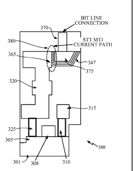
[0030] Referring to Fig. 3A, there is shown a cross-sectional view of a
memory cell
300. The memory cell 300 includes a substrate 301 formed in a first plane and
a metal
connection 320 (e.g., copper, tungsten, etc.) extending in a second plane. The
second
plane is substantially perpendicular to the first plane. The memory cell 300
further
includes a magnetic tunnel junction (MTJ) 365 having a first layer coupled to
the metal
connection 320 such that the first layer of the MTJ 365 is oriented along the
second
plane. As will be appreciated from the illustrated connection, the current
flowing
through the MTJ 365, passes through the interface indicated by 380. Details
regarding
the MTJ 365 will be further discussed in relation to Fig. 3B.
CA 02711305 2010-07-02
WO 2009/089360 PCT/US2009/030451
6
[0031] Referring to Fig. 3B, a more detailed illustration of the vertical
arrangement of
the MTJ 365 is illustrated. The MTJ 365 includes a plurality of layers, such
as a fixed
or pinned layer 362, a tunnel barrier layer 363, and a free layer 364. These
layers can be
formed from films or other methods as will be discussed in greater detail
below.
Further, it will be appreciated that each of these layers may contain one or
more layers
of materials to achieve the functionality of the layer, as discussed above.
For example,
one or more layers of material may be used to form pinned layer 362, however,
the
combination may be referred herein as a single functional layer for
convenience.
[0032] As can be seen from the detailed arrangement of Fig. 3B, each of
the functional
layer (362-364) of the MTJ are oriented along a sidewall of connector 320 in a
vertical
plane (in relation to the substrate). Although the layers (362-364) of the MTJ
365 also
extend horizontal, the current flow through the MTJ 365 is substantially
between
electrode 375 and connector 320 as highlighted by current path 380. The
additional
thickness of the horizontal portions of layers 362-364, particularly of tunnel
barrier
layer 363, aid in directing current flow through vertical interface as
highlighted by
current path 380. Additionally, the sloped portion 347 of the MTJ layers 362-
364 also
maintain the increased layer thickness which inhibits leakage through these
portions and
concentrates the current flow through 380. It will be appreciated that the
sloped profile
aids in establishing the increased layer thickness in the sloped portion 347
of the layers.
[0033] Referring back to Fig. 3A, the MTJ 365 is coupled to a bit line
(not shown) by
the conductor 370 and electrode 375. The metal connection 320 and conductor
325
couple the MTJ 365 to transistor 305. Transistor 305 is coupled to a word line
connection 308 and source line connection via conductors 310 and 315. The
configuration of the memory cell 300 is illustrated in relation to a schematic
diagram in
Fig. 4.
[0034] Fig. 4 illustrates a schematic diagram of the memory cell 300 and
the
relationship to the elements depicted in relation to Figs. 3A and 3B. To
facilitate an
understanding of this relationship, the reference numbers for like elements
have been
maintained. It should be noted that for convenience of illustration that the
physical
orientation of several of the elements, e.g., MTJ 365, transistor 305, etc.
are not
maintained in the schematic diagram. The bit line is couple to the MTJ 365 via
elements 370 and 375. The MTJ 365 is couple to the access / word line
transistor 305
via elements 320 and 325. The word line is coupled to transistor 305 via
element 308
and the source line is coupled to transistor 305 via elements 315 and 310. The
CA 02711305 2010-07-02
WO 2009/089360 PCT/US2009/030451
7
remaining functional aspects of the memory array (e.g., sense amplifier, etc.)
are not
detailed, but are illustrated in Fig. 1, for example, and are known in the
art.
[0035] Referring to Figs. 5-11, an exemplary method of fabricating a
magnetic tunnel
junction (MTJ) 365 in a memory cell 300 according to embodiments of the
invention
will now be described. In Figs. 5-11, the reference numbers for related
elements have
been maintained. Likewise, to avoid redundancy, not all elements will be
discussed in
the description of each figure.
[0036] As illustrated in Fig. 5, an embodiment of the invention can
include two memory
cells having a shared source line connection 310. The additional elements of
the second
cell such as word line connection 309, conductive elements 326 and 321 serve
similar
purposes and accordingly will not be discussed in detail. As discussed above,
the
substrate 301 can be formed in a first plane and a metal connection 320 can be
formed
to extend in a second plane that is substantially perpendicular (e.g.,
vertical) to the first
plane. The metal connection 320 is enveloped in a non-conducting layer 350
(e.g., an
oxide layer). The metal connection 320 and other conductive elements can be
made of a
suitable metal material having good electrical conductive properties such as
copper,
tungsten, aluminum, and the like, as is known in the art.
[0037] Referring to Figs. 6 and 7, once the partial cell structure 300 has
been provided,
a trench 340 can be etched in the oxide layer 350 to expose at least a first
portion of the
metal connection 320, wherein the first portion of the metal connection 320 is
oriented
along the second plane.
[0038] As illustrated in Fig. 6, a photoresist layer 330 having a pattern
of openings 331
may be provided on a top surface of the cells. The openings 331 can be
positioned such
that they overlay a portion 332 of metal connection 320 to ensure that the
first portion of
the metal connection 320 will be exposed. A chemical etchant may then be used
to etch
a trench or cavity 340 in portions of the oxide layer 350 exposed by the
pattern of
openings 331, as shown in Fig. 7. During this first etching step, the pattern
and/or
exposed portion of the metal connection 320 can be controlled in a number of
ways.
For example, process variables such as time the etchant is applied and/or
chemistry of
the etchant can be controlled. Additionally, different patterns can be used to
etch the
trench 340 in the portion of the oxide layer 350 that envelops the metal
connection 320.
[0039] Referring again to Figs. 6 and 7, the oxide layer 350 can be etched
to a desired
depth to expose at least a first portion 322 of the metal connection 320 that
is oriented
along the second plane. Further, the trench or cavity 340 may be formed such
that one
CA 02711305 2010-07-02
WO 2009/089360 PCT/US2009/030451
8
side of the trench 340 is sloped as evident by portion 345. This sloped
portion 345 of
the oxide layer 350, or "slope profile," can be controlled as a function of
any one or
more of the etchant process variables as is known in the art. In other
embodiments, the
parameters may be manipulated to achieve a thinner metal connection 320 in
comparison to the formed cavities 340, or a pattern where the metal connection
320 is
thicker or wider in comparison to the formed trench 340 in which the layers of
the MTJ
are be deposited. Further, the sloped portion 345 facilitates maintaining
thicker layers
in the sloped portion 345 of the MTJ as opposed to the vertical portion 322,
as discussed
above in relation to Fig. 3B.
[0040] Next, as shown in Fig. 8, thin film layers 360 (e.g., 362-364) of
the MTJ 365 can
be deposited in the trench 340 such that a portion of the first layer (e.g.,
362) of the MTJ
365 is oriented along the second plane and such that the first layer of the
MTJ 365 is
coupled to the first portion 322 of the metal connection 320. The thin film
layers 360
which are to form the MTJ 365 may be deposited on top of the cells and within
the
trench 340. These thin film layers 360 may be embodied as thin ferromagnetic
films
including, for example, a pinned layer 362 (e.g., Ta/PtMn/CoFe/Ru/CoFeB), a
tunnel
barrier layer 363 (e.g., AlOx or MgO), and a free layer 364 (e.g., CoFeB/Ta).
One or
more layers of the MTJ 365 may be thinner along the first portion of the metal
connection 320 (i.e., the exposed sidewall 322 of the metal connection 320)
than along
the portions of the trench 340 which are parallel to the substrate 301 or
sloped with
respect to the substrate 301. After deposition of each of the thin film layers
360, which
are to form the MTJ 365, a metal layer 375 may be formed over the thin film
layers 360.
[0041] Referring to Fig. 9, the extraneous thin film layers 360 of the MTJ
365 and the
metal layer 375 can be removed by polishing, such as chemical mechanical
polishing
(CMP), etching (e.g., plasma etching), or other known techniques. As shown in
Fig. 9,
the thin film layers 360 and the metal layer 375 are polished or etched to
substantially
correspond to the upper surface of metal connection 320. The upper surface of
metal
connection 320 can be parallel to the plane of the substrate 301. By removing
the thin
film layers 360 and metal layer 375 overlaying the top surface, the remaining
layers
form the MTJ 365 and electrode 375 and fill in trench 340.
[0042] Referring to Fig. 10, a bit line connection 370 can be formed by a
conductive
element (e.g., a via) on the electrode 375 to electrically couple the
electrode 375, and
hence the MTJ 365, to a bit line (not shown). The conductive element 370 can
be
CA 02711305 2010-07-02
WO 2009/089360 PCT/US2009/030451
9
embedded in a non-conducting layer, which may also overlaid on top of the
electrical
connector 320.
[0043] Referring to Fig. 11, an exemplary arrangement of magnetic tunnel
junctions
(MTJs) in a memory array according to another embodiment of the invention will
now
be described. As shown in Fig. 11, a pair of bit cells 300 and 400 can be
formed as
mirror images of each other. For example, trenches can be etched in the oxide
layer to
expose adjacent first portions of each of the plurality of metal connections
which are in
the second plane. The MTJ layers can be deposited in the trenches formed in
the area
between adjacent pairs of metal connections. It will be appreciated that the
process of
forming the cells 300 and 400 according to Fig. 11 are similar to the
processes
illustrated in Figs. 5-10, and therefore, a detailed explanation is not
provided herein.
Further, it will be appreciated that the process for the dual bit cells can be
applied to
individual bit cells, such as illustrated in Fig. 3A or may be applied to more
than two bit
cells at a time. Accordingly, embodiments of the invention are not limited to
the
illustrated examples provided herein.
[0044] The overall dimensions (e.g., width and/or length) of the junction
area of the
MTJ 365, can be adjusted depending on the desired application of the memory
cell 300.
In other words, the desired pattern can be formed depending on the specifics
of the
particular memory cell 300. In any case, the dimensions of the MTJ 365, and
hence the
memory cell 300, may be a function of the depth of the trench 340 that is
etched into the
oxide layer 350 of the memory cell 300 in order to form the MTJ 365, as well
as the
thickness of the thin film layers 360 to be applied in forming the MTJ 365
during the
above-described deposition process.
[0045] As set forth above, due in part to the physical deposition nature
of this process,
the tunnel barrier thickness in the MTJ 365 may be thinnest near the exposed
first
portion 322 of the metal connection 320 (e.g., as shown in Fig. 7) and thicker
elsewhere
in the trench 340. Accordingly, the tunnel current may primarily pass between
the
metal connection 320 (such as a copper or tungsten) and the electrode 375
through the
vertical portion of the MTJ 365 adjacent 322.
[0046] Accordingly, and unlike conventional processing techniques, only
one or two
photo masks may be used in order to form the STT MRAM cell 300 architecture,
as
exemplarily shown in Figs. 3-10. In the previous examples, a first etching
process is
used to form the trench or cavity 340, and then after the thin film layers 360
of the MTJ
365 and metal layer 375 are deposited, a second etching process, or
alternatively a
CA 02711305 2010-07-02
WO 2009/089360 PCT/US2009/030451
polishing step, is performed to form the MTJ 365 and electrode 375. Moreover,
the
MTJ 365 is formed in a vertical orientation (i.e., oriented in a second plane
that is
perpendicular to the substrate) and its size can be controlled by the hole
dimensions of
the photo mask, the etch depth of the trench 340 and/or the weight of the thin
film layers
360, rather than by use of more or tightly toleranced lithographic controls.
The
manufacturing processes used herein may be compatible to a damascene process
(single
or double) to reduce manufacturing costs. The vertical orientation may provide
improved electrical conduction between the bit line 140 (as shown in Fig. 1)
and the
STT MRAM cells 300 and may provide improved or better adhesion between the MTJ
365 and the metal connection 320, providing a metal-to-metal contact instead
of an
insulation to metal contact as in the conventional STT MRAM cell structure.
[0047] While the foregoing disclosure shows illustrative embodiments of
the invention,
it should be noted that various changes and modifications could be made herein
without
departing from the scope of embodiments of the invention as defined by the
appended
claims. For example, the functions, steps and/or actions of the methods in
accordance
with the embodiments of the invention described herein need not be performed
in any
particular order. Furthermore, although elements of the invention may be
described or
claimed in the singular, the plural is contemplated unless limitation to the
singular is
explicitly stated.