Note: Descriptions are shown in the official language in which they were submitted.
CA 02721674 2016-05-04
THICK FILM HIGH TEMPERATURE THERMOPLASTIC INSULATED
HEATING ELEMENT
FIELD OF THE INVENTION
The present invention relates to a thick film high temperature
thermoplastic insulated resistive heating element suitable for substrates
having a low melting point and/or high coefficient of thermal expansion (CTE)
and a method for producing same using composite coating synthesis
methods.
BACKGROUND OF THE INVENTION
Thick film heating elements have been long sought after because of
their ability to provide versatile designs, high power densities, uniform heat
and rapid heating and cooling. These types of element designs are very
efficient for direct heating either by placing the thick film element in
contact
with the component being heated or when they are required to radiate
directed heat to the surroundings.
A voltage is applied to the resistive thick film either via conductive
tracks or directly to the resistive thick film. This is a desirable element
design,
1
CA 02721674 2010-10-15
WO 2009/129615 PCT/CA2009/000525
as it is low-profile and lightweight, provides rapid heat up and cool down
times, provides very uniform heat, and delivers power at low temperatures
resulting in safer operation of the heating element.
Metal substrates such as aluminum and aluminum alloys and austenitic
grades of stainless steel, such as 300 series stainless (300SS), are desirable
for this application because of their excellent thermal performance
characteristics. Aluminum and aluminum alloys are particularly desirable for
this application because they have a thermal transfer 10 to 20 times that of
stainless steel making thick film heaters on these substrates thermally fast
acting and have a low density making for a very light, efficient heating
element.
Prior art shows an insulating layer (glass enamel) applied to the
substrate to electrically insulate the resistive thick film from the
substrate.
Glass based products produced by companies such as DuPont, Ferro and
(Electro-Science Laboratories, Inc. (ESL) use a combination of melt flowable
glass binder and insulative filler components. Various combinations of metal
oxides in the thick film glass frit lower the melting temperature of the glass
so
that it flows and produces a continuous glass matrix containing the filler
material at suitable firing temperatures.
Typical thick film glass frits are designed to fire at temperatures in
excess of 800 C and are typically used on substrates made of ferritic
stainless
steels, such as 400 series stainless (400SS). However, it is difficult to
produce viable electrically insulating layers on lower temperature metal
substrates such as aluminum and aluminum alloys, which have a low melting
temperature (less than 660 C) or other substrates which have a relatively high
2
CA 02721674 2010-10-15
WO 2009/129615
PCT/CA2009/000525
coefficient of thermal expansion (22-26 ppm/K). Enamel-based insulating
layers commonly used for ferritic stainless steel substrates cannot be used
for
aluminum or aluminum alloy substrates or austenitic stainless steels
substrates, as mismatched thermal expansion coefficients result in cracking of
the electrically insulating layer during initial processing or under thermal
cycling of the heater. Furthermore, these enamel coatings need to be applied
at temperatures typically greater than 600 C, which is too close to the
melting
temperature of the aluminum or aluminum alloy substrates to produce a stable
electrically insulating layer.
Melting temperatures below 600 C can be achieved but have several
limitations. Many of these insulators have lead or Cd in the thick film frits.
However, the thick film formulations used to produce this element must be
lead free in order to comply with the RoHS Directive adopted by Europe in
2006. In addition, these insulators do not have the required dielectric
strength
to meet regulatory safety standards.
Low to no melt flow polymer formulations such as polyimide may be
used to form an electrically insulating layer on low temperature substrate
materials. However, these polymer formulations have either (1) a low
temperature limitation, (2) are not able to transfer the wide range of power
densities required for consumer and industrial heating element applications
into heating the substrate, (3) do not provide the required electrical
insulation
performance, (4) cannot withstand the resistive thick film processing
conditions, or (5) compromise the integrity of the deposited resistive thick
film.
3
CA 02721674 2010-10-15
WO 2009/129615 PCT/CA2009/000525
The above problems with traditional insulating materials necessitate a
unique materials solution for substrates having a low melting point or high
coefficient of thermal expansion (CTE).
SUMMARY OF THE INVENTION
It is the object of the present invention to provide an integrated thick
film heating element on a substrate that may be processed below 600 C so
that it can be used with aluminum, aluminum alloys, low temperature and/or
high CTE substrate materials, has suitable electrical insulation properties
under temperature cycling of about 250 C (or higher) and is capable of
operating over a wide range of power densities for consumer and industrial
heating element applications.
To that end high temperature melt-flowable thermoplastic polymers
mixed with a particulate filler, along with an electrically resistive lead
free thick
film and an electrically conductive electrode track formulations are disclosed
herein that may be deposited and fired to form an integrated thick film
heating
element which may be processed at temperatures below 600 C. This thick
film heating element is capable of operating over a wide range of power
densities for consumer and industrial heating element applications, with
suitable electrical insulation properties under temperature cycling of about
250 C thus making it very useful for integration into a wide range of
commercially useful products.
Particularly, the present invention provides a thick film heating element
comprising a substrate, an electrically insulated dielectric layer comprising
a
high temperature melt flowable thermoplastic polymer/filler material
4
CA 02721674 2010-10-15
WO 2009/129615 PCT/CA2009/000525
composite-, an electrically resistive lead free thick film that can be
produced
by composite sol gel technology, optionally a conductive thick film which is
used to make electrical connection to the resistive element, and optionally a
topcoat which is used to provide further electrical insulation and / or
protection
against moisture and oxidation. This heating element provides efficient and
rapid heat up and cool down, can be designed to provide even temperature
distribution, and delivers power at lower operating temperatures resulting in
increased element safety.
The thick film heating element is cost effective and able to provide a
competitive solution in a wide range of applications. These include but are
not
limited to space heaters, room heaters, device heaters, refrigerator
defrosters,
heated signage, food and beverage warmers and oil warmers to mention just
a few.
In view of the fact that a great many commercial applications use
aluminum or aluminum alloys, composite sol gel conductive and resistive
formulations employed in certain embodiments of this invention have been
selected so that they can be processed at temperatures below 600 C on the
substrates. In addition, these materials do not require the addition of lead
or
any other hazardous material to process the heating element, in keeping with
the RoHS Directive adopted by Europe in 2006.
A dielectric coating comprising an electrically insulating high
temperature thermoplastic polymer/filler material composite layer is deposited
on the substrate and processed below 600 C to form the dielectric layer
coated substrate. The thermoplastic polymer powder is filled with a
particulate
lead-free material that does not exhibit significant melt flow up to the
5
CA 02721674 2010-10-15
WO 2009/129615 PCT/CA2009/000525
processing temperature of the polymer (which should not exceed about 600 C
when aluminum based substrates are used). The filler incorporated into the
thermoplastic layer provides improved thermal expansion coefficient matching
between the high temperature thermoplastic layer and the additionally
deposited electrically resistive lead free thick film and the electrically
conductive electrode track(s).
The filler material integrated into the thermoplastic layer increases the
thermal conductivity of the resulting thermoplastic/filler composite layer to
produce better heat transfer to the substrate and prevents generation of "hot
spots", and provides a bonding layer so that the electrically resistive lead
free
thick film and the electrically conductive electrode track reliably and
consistently do not sink into the insulating thermoplastic/filler composite
layer
when any of the additionally deposited resistive lead free thick films or
electrically conductive electrode tracks are processed to a temperature near
or above the melting temperature of the high temperature thermoplastic
matrix, to avoid compromising the integrity of the electrical insulation.
A composite sol gel resistive thick film is then deposited on the coated
substrate and processed to form a thick film heating element. The
constituents of the sol gel are selected so that they can be processed below
600 C in the case where the substrate is aluminum, aluminum alloys or the
like. Voltage can be applied directly to this resistor or through a conductive
track that connects to the resistive thick film and is also deposited onto the
insulated dielectric layer coated substrate at a temperature below 600 C. If
necessary, a topcoat layer may be deposited onto the electrically resistive
6
CA 02721674 2010-10-15
WO 2009/129615 PCT/CA2009/000525
heater layer to provide oxidation protection, moisture resistance and
electrical
insulation for the integrated heater element.
Thus, in one aspect of the invention there is provided a lead free thick
film heating element on a substrate, comprising:
a dielectric coating located on said surface, said dielectric coating
being made from an electrically insulating melt flowable high temperature
thermoplastic polymer mixed with a pre-selected amount of a filler material;
and
an electrically resistive lead free thick film located on said dielectric
coating having a resistance, such that when the voltage is applied to said
electrically resistive lead free thick film it responsively heats.
The present invention provides a process for producing a sealed,
electrically insulating thermoplastic based coating on a surface of a
substrate
comprising the steps of:
a) producing a dielectric coating on said surface of the substrate by
i) mixing a melt flowable high temperature thermoplastic polymer
powder and a pre-selected amount of powder filler material in a
solution to form a uniform stable dispersion;
ii) applying said uniform stable dispersion to a surface of the
substrate so as to provide a coating thereon;
iii) thermally processing said coated substrate at a temperature
sufficient to remove any volatile and/or organic components from said
uniform stable dispersion and melt flow the thermoplastic polymer
powder and produce at least one electrically insulating coating
containing the filler material on said substrate;
7
CA 02721674 2010-10-15
WO 2009/129615 PCT/CA2009/000525
b) depositing an electrically resistive lead free thick film formulation
onto a top surface of said at least one electrically insulating coating and
thermally processing said electrically resistive lead free thick film
formulation
to produce an electrically resistive lead free thick film; and
c) applying an electrical conductor in electrical contact with said
electrically resistive lead free thick film for applying electrical power to
said
electrically resistive lead free thick film to heat it.
The present invention also provides an article having a heated metal
component, comprising:
a) an article having a metal component configured to contact another
article, the metal component having a surface;
b) a lead free thick film heating element formed on the surface of the
metal component for heating said metal component, said lead free thick film
heating element including
i) a dielectric coating located on said surface, said dielectric
coating being an electrically insulating melt flowable high temperature
thermoplastic based thick film containing a pre-selected amount of a
filler material;
ii) an electrically resistive lead free thick film located on said
dielectric coating,
iii) an electrical conductor in electrical contact with said
electrically resistive lead free thick film; and
c) a battery connected to said electrical conductor and a switch for
electrically connecting said battery to said electrical conductor such that
when
8
CA 02721674 2010-10-15
WO 2009/129615 PCT/CA2009/000525
said switch is turned on a voltage is applied through said electrical
conductor
so that said electrically resistive lead free thick film is heated.
A further understanding of the functional and advantageous aspects of
the invention can be realized by reference to the following detailed
description
and drawings.
BRIEF DESCRIPTION OF THE DRAWINGS
The invention will be more fully understood from the following detailed
description thereof taken in connection with the accompanying drawings,
which form a part of this application, and in which:
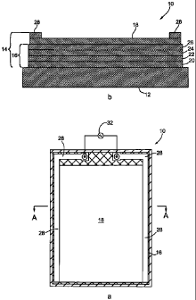
Figure la is a top view of an embodiment of a thick film high
temperature thermoplastic insulated heating element constructed in
accordance with the present invention;
Figure lb is a cross sectional view of heating element of Figure la
taken along the line A-A;
Figure 2a is a top view of another embodiment of a thick film high
temperature thermoplastic insulated heating element constructed in
accordance with the present invention; and
Figure 2b is a cross sectional view of heating element of Figure 2a
taken along the line B-B.
9
CA 02721674 2010-10-15
WO 2009/129615 PCT/CA2009/000525
DETAILED DESCRIPTION OF THE INVENTION
Generally speaking, the systems described herein are directed to a
thick film high temperature thermoplastic insulated substrate-based heating
element and a method for producing same using composite coating synthesis
methods. As required, embodiments of the present invention are disclosed
herein. However, the disclosed embodiments are merely exemplary, and it
should be understood that the invention may be embodied in many various
and alternative forms, including substitution of the metal substrate with
another material such as glass or ceramic that may require further electrical
insulation or leakage current reduction to satisfy operating requirements for
the integrated thick film heating element.
Therefore, specific structural and functional details disclosed herein are
not to be interpreted as limiting but merely as a basis for the claims and as
a
representative basis for teaching one skilled in the art to variously employ
the
present invention. The figures are not to scale. For purposes of teaching and
not limitation, the illustrated embodiments are directed to a thick film high
temperature thermoplastic insulated metal based heating element and a
method for producing same using composite coating synthesis methods.
As used herein, the term "about", when used in conjunction with ranges
of dimensions of particles or other physical properties or characteristics, is
meant to cover slight variations that may exist in the upper and lower limits
of
the ranges of dimensions so as to not exclude embodiments where on
average most of the dimensions are satisfied but where statistically
dimensions may exist outside this region. It is not the intention to exclude
embodiments such as these from the present invention.
CA 02721674 2010-10-15
WO 2009/129615 PCT/CA2009/000525
As used herein, the phrase "electrically insulating melt flowable high
temperature thermoplastic based thick film" means that a specified voltage
may be applied across the thickness dimension of the thick film and electrical
breakdown or unacceptable level of leakage current does not occur such that
the film is termed electrically insulating, that the film structure includes a
melt
flowable thermoplastic matrix formed from melt flowable thermoplastic
powders at a temperature typically above 250 C, and that the thick film
structure withstands high temperatures, maintaining a solid structure at
operating temperatures exceeding 180 C.
The term "thick film" as used herein is meant to refer to coatings that in
general are >1 urn in thickness. While the terms "thick films" and "thin
films"
are relative, in the coatings industry, "thin film" generally refers to
technologies
using nano or submicron thick coatings typically done for optical and
electronic applications using techniques such as sputtering, PVD, MBE etc.
which in some cases lay down atomic thick layers of the coating. On the other
hand, "thick film" generally refers to technologies used for coatings that are
>1 urn and may be produced by deposition of several successive layers using
techniques such as screen printing process. While "thick film" generally
refers
to films with a thickness in the range from about 1 to about 500 urn which
would cover the range for most commercial article heating applications, it
will
be appreciated that thicker films e.g about 1000 um or thicker are also
covered by the term "thick film".
It will be understood that when referring to a dielectric coating located
on the surface of a substrate which is made from an electrically insulating
melt
flowable high temperature thermoplastic polymer mixed with a pre-selected
11
CA 02721674 2010-10-15
WO 2009/129615 PCT/CA2009/000525
amount of a filler material, it will be understood that this "dielectric
coating"
may be a monolithic coating deposited in a single deposition process.
Alternatively, it can also be understood to mean that the "dielectric coating"
may comprise two or more coatings deposited and cured one on top of the
other so that the "dielectric coating" is in fact two or more coatings used to
build up the "dielectric coating". The amount of filler may be the same in
each
of the coatings or it may be varied for one or more of these multiple
coatings.
When referring to processing temperatures for both the dielectric
coating and the electrically resistive lead free thick film grown on top of
the
dielectric coating, it will be understood that the temperatures disclosed
herein
are exemplary only and not limited to those temperatures or temperature
ranges. The temperatures that can be used will depend on the melt flowable
high temperature thermoplastic polymer being used, the filler material being
mixed with the thermoplastic polymer, the particular materials used to produce
the electrically resistive lead free thick film, and the nature of the
substrate.
For example, when the substrates on which the heater elements are being
formed are made from aluminum or aluminum alloys then an upper limit of
around 600 C since the melting point of these materials is around 600 C.
Other the other hand, if stainless steels are the substrate material,
processing
temperatures higher than 600 C could be used but in this case the processing
temperatures would be dependent more so on the nature of the thermoplastic
polymer being used, the filler material and the materials used to make the
electrically resistive lead free thick film.
Figures la and lb illustrate an embodiment of the combined
heater/substrate device shown generally at 10. More particularly, Figure la
12
CA 02721674 2010-10-15
WO 2009/129615 PCT/CA2009/000525
shows a top view of the combined heater element 14/substrate 12 shown in
Figure lb and Figure 1b shows a cross section of the combination. The
substrate 12, which is preferably metal such as used in many commercial
products and may be made of aluminum, aluminum alloys, or stainless steels
of any grade or quality. However, it will be appreciated that the substrate 12
may be of any material so long as it has a melting point above the maximum
temperature that can be produced by the heater itself.
The heater element 14 is lead (and cadmium) free and may withstand
temperatures of e.g. 500 C. The surface of substrate 12 may be treated to
provide improved uniformity and adhesion of the coating layers from
deposition to thermal processing to heating element operation. Examples of
the surface treatment of the surface of the substrate include sanding, rubbing
and sandblasting.
Heater component 14 as shown in Figure lb includes an insulating
dielectric layer 16, and electrically resistive heater layer 18 on the
dielectric
layer 16, and two conductive strips/bus bars 28 located on the peripheral
edge of resistive heater layer 18. A preferred embodiment of insulating
dielectric layer 16 as shown in Figures lb and 2b comprises four (4) separate
insulating dielectric layers 20, 22, 24 and 26 with layer 20 located on the
surface of substrate 12, layer 22 on layer 20, layer 24 on layer 22 and layer
26 on layer 24.
Dielectric layer 16 is an electrically insulating melt flowable high
temperature thermoplastic based thick film. This electrically insulating
dielectric layer 16 is made from a formulation containing a combination of
high
temperature melt flowable thermoplastic powders and filler materials in a
13
CA 02721674 2010-10-15
WO 2009/129615 PCT/CA2009/000525
suitable vehicle which includes various volatile and/or organic constituents,
for
deposition, which may be deposited and thermally processed to a
temperature in the range of 300-450 C to melt flow the thermoplastic powder
and form a cohesive composite coating with the filler particles embedded in a
bonded thermoplastic matrix that is adhered to the substrate (which in many
commercial embodiments may be a metal substrate). In an embodiment of the
device, dielectric layers 20, 22 and 24 may be identical and layer 26 may be
of a different composition from the other three.
While there are four layers shown, there may be more or less layers
and the present device is not restricted to four layers. Depositing the
overall
dielectric layer 16 in four layers is to minimize the effect of pinholes on
the
overall electrical insulation properties of the coating and to ensure that the
various volatile organic constituents in the carrier are removed during
baking.
Each layer is deposited or coated by being printed (for example), then fired
to
form a rigid layer with all the volatile organic constituents removed except
of
course the melt flowable organic material itself, and then the next layer is
deposited until all four layers are laid down. This process has been found to
ensure good quality dielectric layers.
The four insulating dielectric layers 20, 22, 24 and 26 are produced
from a melt flowable high temperature thermoplastic polymer which comprises
at least one of polyphenylene sulfide (PPS), polyphthalamide (PPA),
polyarylamide (PARA), liquid crystal polymer, polysulfone (PS),
polyethersulfone (PES), polyphenylsulfone (PPSU, polyamide-imide (PAI),
polyetheretherketone (PEEK), polyetherketone (PEK),
14
CA 02721674 2010-10-15
WO 2009/129615 PCT/CA2009/000525
polyetherketoneetherketone (PEKEK) or self reinforced polyphenylene (SRP),
and any combination of these may be used.
Figures 2a and 2b show another embodiment of a heater element at
40 which is similar to element 10 of Figure la, lb with the exception that the
heater element 14' now includes a top coat 42 located on top of the
electrically resistive heater layer 18. In addition, the conductive
strips/buss
bars 28 are deposited directly onto the upper peripheral edge of dielectric
layer 26 and the electrically resistive heater layer 18 is coated on top of
layer
26/bus bars 28 as shown in Figure 2b. A topcoat 42, which is electrically
insulating and preferably contains ceramic, glass or low melt flow high
temperature polymer filler particles (fluoropolymers, siloxanes, silicones,
polyimides, etc.), may be optionally deposited onto the resistive and
conductive thick films to provide oxidation protection and/or to ensure that
the
element is not affected by water.
In both embodiments of the heater illustrated in Figures la to 2b, the
electrically resistive heater layer 18 is uniformly heated by application of a
voltage to layer 18 through the conductive tracks 28 using a power source 32
in Figures la and 2a, which typically is a small battery which is usually flat
or
has a low profile so that it can be hidden on the commercial product.
The insulating dielectric layer 16 is important for the development of a
functional heater for use on commercial products such as razor blades and
hair irons. The primary requirement for the insulating dielectric layer 16 is
high
electrical insulation strength and high thermal conductivity, while at the
same
time the dielectric layer 16 must be deposited in such a way as to avoid pin
CA 02721674 2010-10-15
WO 2009/129615 PCT/CA2009/000525
holes. This is achieved by development of both appropriate formulations and
proper processing parameters.
The melt flowable high temperature thermoplastic polymer layers are
formulated using thermoplastic polymer powder particles which have a
particle size in the range from about 1 to about 100 microns, and preferably
has a particle size of from about 1 to about 20 microns. The powder size plays
an important role in producing a uniform dispersion and even melt flow during
processing. Combinations of melt flowable thermoplastic polymer powders
were tested to improve dispersion and melt flow characteristics and wetting of
filler, e.g., addition of PAI to PEEK was found to improve dielectric
properties.
The filler material may include ceramics, glass or high temperature
polymer particles. The filler material may have a particle size in the range
from about 0.1 microns to about 100 microns, and preferably in a range from
about 1 to about 20 microns. In each of the base dielectric layers 20, 22 and
24, the filler is present in the polymer in a range from about 5-80 weight
percent and preferably in a range from about 20-60 weight percent, and most
preferably it is present in an amount of about 35-45 weight percent.
The powder filler material is added to the melt flowable high
temperature thermoplastic powder and has the following functions. First, it
provides improved thermal expansion coefficient matching between the high
temperature thermoplastic layer and the additionally deposited resistive and
conductive thick films both during initial processing and during electrical
cycling operation of the integrated heating element. Secondly, the filler
increases the thermal conductivity of the insulating layer to produce better
heat transfer to the metal substrate and prevent generation of "hot-spots" in
16
CA 02721674 2010-10-15
WO 2009/129615 PCT/CA2009/000525
the resistive layer during operation of the heater. Third, with the presence
of
the filler in the dielectric layer, additionally deposited resistive or
conductive
thick films on the top of layer 26 reliably and consistently do not sink into
the
insulating thermoplastic layer 16 when any of these additionally deposited
resistive or conductive thick films are processed to a temperature near or
above the melting temperature of the high temperature thermoplastic matrix,
compromising the integrity of electrical insulation.
Thus the filler particles serve to reinforce the layer 16. Examples of
suitable ceramic materials include alumina, zirconia, silica, (optionally
ceria
stabilized zirconia or yttria stabilized zirconia), titania, calcium
zirconate,
silicon carbide, titanium nitride, nickel zinc ferrite, calcium hydroxyapatite
and
any combinations thereof. Alumina has the highest thermal conductivity and
dielectric strength.
It has been observed that layering of base dielectric layer 16 such as
illustrated in Figures lb and 2b is preferred to achieve a minimum thickness
of 180pm to obtain 3000V hi-pot strength at 250 C as required by regulatory
standards such as IEC 60335 (International Electrotechnical Commission).
This can require up to 6 layers to achieve when spray or screen printing.
Each layer is processed below 600 C, typically to 400-450 C to cure the
coating the coating.
Alternatively, a thick film of the required thickness, required
composition and filler loading can be placed directly on the substrate prior
to
processing at temperatures in the range from about 400 to about 450 C.
Thermal processing is performed in air using conventional furnace or IR
heating may be used. An advantage of the present heater element over glass
17
CA 02721674 2010-10-15
WO 2009/129615
PCT/CA2009/000525
frit dielectric based heaters is that in the present device the processing
parameters to get melt flow are not critical and the furnace profile is not
critical, unlike the conditions required with glass frit dielectric based
heaters.
Top dielectric layer 26 is added to the base dielectric layers 20, 22 and
24 to provide a bonding layer which adheres to the electrically resistive
heater
layer 18 and conductive strips 28. Upper most layer 26, while made of the
same thermoplastic polymer as the based dielectric layers 20, 22 and 24, has
a higher filler loading than these base dielectric layers, up to 95% by
weight,
and can be applied and processed in the same was as the base dielectric
layers 20, 22 and 24.
In the top dielectric layer 26, the filler is present in the polymer in a
range from about 5-95 weight percent and preferably in a range from about
40-80 weight percent, and most preferably it is present in an amount of about
60-70 weight percent. The top dielectric layer 26 is also useful in that it
provides increased mechanical stability and improved coefficient of thermal
expansion (CTE) which facilitates a much better thermal matching to the
insulating dielectric layers 20, 22 and 24 and electrically resistive heater
layer
18 both during processing and subsequent operation under applied electrical
power at elevated temperatures.
A lead-free composite sol gel based electrically resistive heater layer
18 is deposited onto the thermoplastic composite coating and processed
(fired) to a temperature below 600 C, typically in the range from about 400 to
about 450 C (but not limited thereto) to cure the coating. The temperature is
selected to give a crack-free layer 18 free of volatile and/or organic
constituents. The composite sol gel resistive thick layer 18 may be made
18
CA 02721674 2010-10-15
WO 2009/129615 PCT/CA2009/000525
according to the teachings of United States Patent No. 6,736,997 issued on
May 18, 2004 and United States Patent No. 7,459,104 issued Dec. 2, 2008
both to aiding et al., (which are incorporated herein in their entirety by
reference) and the resistive powder can be one or graphite, silver, nickel,
doped tin oxide or any other suitable resistive material, as described in the
Olding patent publication.
The sol gel formulation is a solution containing reactive metal organic
or metal salt sol gel precursors that are thermally processed to form a
ceramic
material such as alumina, silica, zirconia, (optionally ceria stabilized
zirconia
or yttria stabilized zirconia), titania, calcium zirconate, silicon carbide,
titanium
nitride, nickel zinc ferrite, calcium hydroxyapatite and any combinations
thereof. or combinations thereof. The sol gel process involves the preparation
of a stable liquid solution or "sol" containing inorganic metal salts or metal
organic compounds such as metal alkoxides. The sol is then deposited on a
substrate material and undergoes a transition to form a solid gel phase. With
further drying and firing at elevated temperatures, the "gel" is converted
into a
ceramic coating.
The sol gel formulation may be an organometallic solution or a salt
solution. The sol gel formulation may be an aqueous solution, an organic
solution or mixtures thereof.
A lead-free conductive thick film can be used to make the conductive
strips/buss bars 28 for making an electrical connection to the resistive thick
film element 18. This conductive strips 28 are deposited either before (see
Figure 2b) or after deposition of the resistive coating (see Figure 1b). It
can
be processed using a separate processing step at a temperature of 450 C or
19
CA 02721674 2010-10-15
WO 2009/129615 PCT/CA2009/000525
less or alternatively it can be co-fired with the resistive thick film 18. The
lead-
free conductive thick film can be made from a composite sol gel formulation
that contains nickel, silver or any other suitable conductive powder or flake
material. The sol gel formulation may be prepared from, but is not limited to,
alumina, silica, zirconia, or titania metal organic precursors stabilized in
solution.
Alternately, the conductive track 28 may be produced from any
commercially available thick film product that is lead-free and can be
thermally
processed at a temperature of 450 C or less. One suitable thick film product
is Parmod VLT from Parelec, Inc. which contains a reactive silver metal
organic, and silver flake or powder dispersed in a vehicle and can be fired at
a
temperature typically between 200-450 C. While Parmod VLT is a preferred
commercially available conductive thick film product, it should be understood
that other suitable conductive thick film products may be used, and that the
present invention is not limited to these example products. Since the
conductive film may not be exposed to the heating temperatures in the
resistive thick film, some high temperature polyimide or polyamide-imide
based silver thick film products may also be suitable for use in producing the
conductive thick film track 28.
The present invention will now be illustrated with the following non-
limiting examples. It will be appreciated that these examples and the
processing conditions for making the heater elements are for purposes of
illustration only and not meant to limit the scope of the present invention.
For
example, the substrates used, the constituents used to make each of the
different layers will determine the processing temperatures but it will be
CA 02721674 2010-10-15
WO 2009/129615 PCT/CA2009/000525
appreciated that variations in substrate material, thermoplastic polymer,
filler
material, resistive heater layer composition may be accompanied by different
processing temperatures and other conditions.
EXAMPLE 1
A thick film thermoplastic insulated resistive heating element 40 as
shown in Figure 2b is fabricated on a 304 SS substrate material 12 by
depositing and processing the three dielectric layers 20, 22 and 24 of base
dielectric to 400 C, using a formulation comprising a ratio of 25 parts
Victrex
704 PEEK powder, 4 parts Solvay TorIon Al-50 PAI powder, and 15 parts
P662B alumina powder by weight in a uniform stable dispersion. While Victrex
704 PEEK and TorIon PAI are preferred powders, it should be understood that
other suitable commercially available powders may be used, and that the
present invention is not limited to these example products. A single layer top
dielectric 26 is deposited and processed to 400 C, using a formulation
comprising a ratio of 7 parts Vicote 704 PEEK powder to 13 parts of P662B
alumina powder by weight in a uniform stable dispersion. A lead free
conductive thick film track 28 is deposited and processed to 400 C using
Parmod VLT, a commercially available lead free thick film silver ink. A lead
free resistive thick film 18 is deposited and processed to 400 C, using a
formulation comprising graphite powder dispersed in an alumina-based sol-
gel solution. The electrically resistive thick film 18 is deposited on the
thermoplastic based dielectric insulated metal substrate 26/24/22/20 such that
it makes contact with the conductive track 28 to form the thick film heating
element 40.
21
CA 02721674 2010-10-15
WO 2009/129615
PCT/CA2009/000525
A topcoat formulation containing 35 parts Vicote 704 PEEK powder,
2.2 parts Solvay TorIon Al-50 PAI powder, and 15 parts P662B alumina
powder by weight in a uniform stable dispersion is deposited onto the heating
element to provide top coat 42 to give both moisture protection and oxidation
resistance. This topcoat 42 is processed to 400 C. Wire connectors are then
attached to the thick film heating element 40 which are connected to a power
source 32 as shown in Figure 2a. When a voltage V is applied to the heating
element 40, the element heats up according to input power V2/R, where R is
the resistance of the heating element. The heating element 40 passes a 3.5
kV AC room temperature hi-pot test for 60 seconds, and is capable of
continuous operation at about 250 C.
EXAMPLE 2
A thick film thermoplastic insulated resistive heating element is made
according to Example 1, but the conductive track 28 is deposited and
processed to 400 C using a lead free silver thick film formulation comprising
a
silver flake dispersed in a silica-based sol gel solution.
EXAMPLE 3
A thick film thermoplastic insulated resistive heating element is made
according to Example 1, but the substrate material 12 is aluminum instead of
304SS.
22
CA 02721674 2010-10-15
WO 2009/129615 PCT/CA2009/000525
EXAMPLE 4
A thick film thermoplastic insulated resistive heating element is made
according to Example 1, but the resistive thick film 18 is deposited before
the
conductive track 28 so that the track 28 is deposited on top of thick film 18
to
give the structure of Figure lb.
EXAMPLE 5
A thick film thermoplastic insulated resistive heating element is made
according to Example 1, but both the conductive track 28 and resistive thick
film 18 were deposited before processing to 400 C.
EXAMPLE 6
A thick film thermoplastic insulated resistive heating element is made
according to Example 1, but the conductive track 28 and resistive thick film
18 are processed to 450 C.
EXAMPLE 7
A thick film thermoplastic insulated resistive heating element is made
according to Example 1, except that a topcoat 42 is not included to give the
structure 10 of Figure lb but with the conductive track 28 as shown in Figure
2b.
EXAMPLE 8
A thick film thermoplastic insulated resistive heating element is made
according to Example 1, except that four layers of base dielectric having the
23
CA 02721674 2010-10-15
WO 2009/129615 PCT/CA2009/000525
same composition such as layers 24/22/20 are deposited and processed to
400 C and a top dielectric layer such as layer 26 is not included. The top
layer
of base dielectric in this example does not contain PAI, as it can react with
the
silver film track causing an electrical failure in the track during heating
element
operation.
EXAMPLE 9
A thick film thermoplastic insulated resistive heating element is made
by depositing and processing the base 24/22/20 and top 26 dielectric layers
as in Example 1. A resistive thick film track is then deposited and processed
to 400 C using a formulation comprising silver flake in an alumina sol-gel
solution. The length and width of the silver track are set to give the
required
resistance. In this example, the resistive track of silver (or it may be
graphite
based, replaces both the electrically resistive layer 18 and conductive track
28
as it's dimensions and resistivity are selected such that it acts as both and
it is
laid in an elongate track pattern across the surface so as to be able to heat
the surface up. Electrical contact is made to the two ends of this resistive
track.
EXAMPLE 10
A thick film thermoplastic insulated resistive heating element is made
according to Example 8, except that the formulation for the four deposited
base dielectric layers is comprising 40 parts RytonTM PPS powder, 40 parts
P662B alumina powder and 1 part fumed silica by weight in a uniform stable
dispersion. (four dielectric layers of same composition as 24, 22, 20. The
24
CA 02721674 2010-10-15
WO 2009/129615
PCT/CA2009/000525
heating element passes a 3.5 kV AC room temperature hi-pot test for 60
seconds.
As used herein, the terms "comprises", "comprising", "including" and
"includes" are to be construed as being inclusive and open ended, and not
exclusive. Specifically, when used in this specification including claims, the
terms "comprises" and "comprising" and variations thereof mean the specified
features, steps or components are included. These terms are not to be
interpreted to exclude the presence of other features, steps or components.
The foregoing description of the preferred embodiments of the
invention has been presented to illustrate the principles of the invention and
not to limit the invention to the particular embodiment illustrated. It is
intended
that the scope of the invention be defined by all of the embodiments
encompassed within the following claims and their equivalents.