Note: Descriptions are shown in the official language in which they were submitted.
CA 02726120 2010-11-26
WO 2009/154957 PCT/US2009/045186
FRONT LIGHT DEVICES AND METHODS OF FABRICATION THEREOF
REFERENCE TO RELATED APPLICATIONS
[0001] The present application claims priority to U.S. Provisional Application
No.
61/056,601, filed May 28, 2008.
BACKGROUND
Field of the Invention
[0002] The present invention relates to microelectromechanical systems (MEMS).
Description of the Related Art
[0003] Microelectromechanical systems (MEMS) include micro mechanical
elements, actuators, and electronics. Micromechanical elements may be created
using
deposition, etching, and/or other micromachining processes that etch away
parts of substrates
and/or deposited material layers or that add layers to form electrical and
electromechanical
devices. One type of MEMS device is called an interferometric modulator. As
used herein,
the term interferometric modulator or interferometric light modulator refers
to a device that
selectively absorbs and/or reflects light using the principles of optical
interference. In certain
embodiments, an interferometric modulator may comprise a pair of conductive
plates, one or
both of which may be transparent and/or reflective in whole or part and
capable of relative
motion upon application of an appropriate electrical signal. In a particular
embodiment, one
plate may comprise a stationary layer deposited on a substrate and the other
plate may
comprise a metallic membrane separated from the stationary layer by an air
gap. As
described herein in more detail, the position of one plate in relation to
another can change the
optical interference of light incident on the interferometric modulator. Such
devices have a
wide range of applications, and it would be beneficial in the art to utilize
and/or modify the
characteristics of these types of devices so that their features can be
exploited in improving
existing products and creating new products that have not yet been developed.
SUMMARY
[0004] In one embodiment, an illumination device comprises a light guide
having
a first end for receiving light and configured to support propagation of light
along the length
of the light guide. A turning microstructure is disposed on a first side of
the light guide
1
CA 02726120 2010-11-26
WO 2009/154957 PCT/US2009/045186
configured to turn light incident on the first side and to direct the light
out a second opposite
side of the light guide, wherein the turning microstructure comprises a
plurality of
indentations. A cover is physically coupled to the light guide and disposed
over the turning
microstructure. An interlayer is between the cover and the light guide,
wherein the interlayer
physically couples the cover to the light guide. A plurality of open regions
is between the
interlayer and the plurality of indentations, wherein the light guide has a
first index of
refraction and the interlayer has a second index of refraction and the second
index of
refraction is lower than the first index of refraction.
[0005] In another embodiment, an illumination device comprises a light guide
having a first end for receiving light and configured to support propagation
of light along the
length of the light guide. A turning microstructure is disposed on a first
side of the light
guide configured to turn light incident on the first side and to direct the
light out a second
opposite side of the light guide, wherein the turning microstructure comprises
a plurality of
indentations. A cover is physically coupled to the light guide and disposed
over the turning
microstructure. An interlayer is between the cover and the light guide,
wherein the interlayer
physically couples the cover to the light guide. A plurality of regions is
between the
interlayer and the plurality of indentations at least partially comprising a
material different
from the interlayer.
[00061 In another embodiment, an illumination device comprises a light guide
having a first end for receiving light and configured to support propagation
of light along the
length of the light guide. A turning microstructure is disposed on a first
side of the light
guide configured to turn light incident on the first side and to direct the
light out a second
opposite side of the light guide, wherein the turning microstructure comprises
a plurality of
indentations. A cover is physically coupled to the light guide and disposed
over the turning
microstructure. A plurality of open regions is between the cover and the
plurality of
indentations, wherein the light guide has a first index of refraction and the
cover has a second
index of refraction and the second index of refraction is lower than the first
index of
refraction.
[0007] In another embodiment, a method of manufacturing a illumination device
comprises providing a light guide having a first end for receiving light and
configured to
2
CA 02726120 2010-11-26
WO 2009/154957 PCT/US2009/045186
support propagation of light along the length of the light guide, said light
guide having
turning microstructure disposed on a first side thereof that is configured to
turn light incident
on the first side and to direct the light out a second opposite side of the
light guide, wherein
the turning microstructure comprises a plurality of indentations. The method
also comprises
providing a cover disposed over the turning microstructure. The method also
comprises
physically coupling the cover to the light guide by an interlayer such that a
plurality of open
regions are between the interlayer and the plurality of indentations, wherein
the light guide
has a first index of refraction and the interlayer has a second index of
refraction and the
second index of refraction is lower than the first index of refraction.
[0008] In another embodiment, a method of manufacturing a illumination device
comprises providing a light guide having a first end for receiving light and
configured to
support propagation of light along the length of the light guide, said light
guide having
turning microstructure disposed on a first side thereof that is configured to
turn light incident
on the first side and to direct the light out a second opposite side of the
light guide, wherein
the turning microstructure comprises a plurality of indentations. The method
also comprises
providing a cover disposed over the turning microstructure. The method also
comprises
physically coupling the cover to the light guide by an interlayer such that a
plurality of
regions between the interlayer and the plurality of indentations at least
partially comprises a
material different from the interlayer.
[0009] In another embodiment, a method of manufacturing a illumination device
comprises providing a light guide having a first end for receiving light and
configured to
support propagation of light along the length of the light guide, said light
guide having
turning microstructure disposed on a first side thereof that is configured to
turn light incident
on the first side and to direct the light out a second opposite side of the
light guide, wherein
the turning microstructure comprises a plurality of indentations. The method
also comprises
physically coupling a cover to the light guide, wherein the cover is disposed
over the turning
microstructure, and wherein the light guide has a first index of refraction
and the cover has a
second index of refraction and the second index of refraction is lower than
the first index of
refraction.
3
CA 02726120 2010-11-26
WO 2009/154957 PCT/US2009/045186
[0010] In another embodiment, an illumination device comprises a means for
turning light having a first end for receiving light and configured to support
propagation of
light along the length of the light guiding means. A means for turning light
is disposed on a
first side of the light guiding means configured to turn light incident on the
first side and to
direct the light out a second opposite side of the light guiding means,
wherein the turning
means comprises a plurality of means for reflecting light. A means for
covering is physically
coupled to the light guiding means and disposed over the turning means. The
device
comprises a means for physically coupling the covering means to the light
guiding means. A
plurality of open regions are between the covering means and the plurality of
reflecting
means, wherein the light guiding means has a first index of refraction and the
coupling means
has a second index of refraction and the second index of refraction is lower
than the first
index of refraction.
[0011] In another embodiment, an illumination device comprises a means for
turning light having a first end for receiving light and configured to support
propagation of
light along the length of the light guiding means. A means for turning light
is disposed on a
first side of the light guiding means configured to turn light incident on the
first side and to
direct the light out a second opposite side of the light guiding means,
wherein the turning
means comprises a plurality of means for reflecting light. A means for
covering is physically
coupled to the light guiding means and disposed over the turning means. The
device
comprises a means for physically coupling the covering means to the light
guiding means. A
plurality of regions are between the covering means and the plurality of
reflecting means at
least partially comprising a material different from the coupling means.
[0012] In another embodiment, an illumination device comprises a means for
turning light having a first end for receiving light and configured to support
propagation of
light along the length of the light guiding means. A means for turning light
is disposed on a
first side of the light guiding means configured to turn light incident on the
first side and to
direct the light out a second opposite side of the light guiding means,
wherein the turning
means comprises a plurality of means for reflecting light. A means for
covering is physically
coupled to the light guiding means and disposed over the turning means. A
plurality of open
regions are between the covering means and the plurality of reflecting means,
wherein the
4
CA 02726120 2010-11-26
WO 2009/154957 PCT/US2009/045186
light guiding means has a first index of refraction and the covering means has
a second index
of refraction and the second index of refraction is lower than the first index
of refraction.
BRIEF DESCRIPTION OF THE DRAWINGS
[0013] FIG. 1 is an isometric view depicting a portion of one embodiment of an
interferometric modulator display in which a movable reflective layer of a
first
interferometric modulator is in a relaxed position and a movable reflective
layer of a second
interferometric modulator is in an actuated position.
[0014] FIG. 2 is a system block diagram illustrating one embodiment of an
electronic device incorporating a 3x3 interferometric modulator display.
[0015] FIG. 3 is a diagram of movable mirror position versus applied voltage
for
one exemplary embodiment of an interferometric modulator of FIG. 1.
[0016] FIG. 4 is an illustration of a set of row and column voltages that may
be
used to drive an interferometric modulator display.
[0017] FIG. 5A illustrates one exemplary frame of display data in the 3x3
interferometric modulator display of FIG. 2.
[0018] FIG. 5B illustrates one exemplary timing diagram for row and column
signals that may be used to write the frame of FIG. 5A.
[0019] FIGS. 6A and 6B are system block diagrams illustrating an embodiment of
a visual display device comprising a plurality of interferometric modulators.
[0020] FIG. 7A is a cross section of the device of FIG. 1.
[0021] FIG. 7B is a cross section of an alternative embodiment of an
interferometric modulator.
[0022] FIG. 7C is a cross section of another alternative embodiment of an
interferometric modulator.
[0023] FIG. 7D is a cross section of yet another alternative embodiment of an
interferometric modulator.
[0024] FIG. 7E is a cross section of an additional alternative embodiment of
an
interferometric modulator.
CA 02726120 2010-11-26
WO 2009/154957 PCT/US2009/045186
[0025] FIG. 8A is a cross section of an embodiment of a display device
comprising a prismatic turning microstructure, a light guide panel and a
display panel.
[0026] FIG. 8B is a cross section of a portion of another embodiment of a
display
device comprising a diffractive turning microstructure, a light guide panel
and a display
panel.
[0027] FIG. 9A is a cross section of an embodiment of a display device
comprising a cover layer, a turning microstructure, a light guide panel and a
display panel.
[0028] FIG. 9B is a cross section of another embodiment of a display device
comprising a cover layer, an adhesive layer, a turning microstructure, a light
guide panel and
a display panel.
[0029] FIG. 9C is a cross section of another embodiment of a display device
comprising a cover layer, an adhesive layer, a turning microstructure, a
plurality of diffractive
regions, a light guide panel and a display panel.
[0030] FIG. 10A is a cross section of an embodiment of a display device
comprising a cover layer, an adhesive layer, a turning microstructure, a
plurality of filled
regions, a light guide panel and a display panel.
[0031] FIG. 10B is a cross section of another embodiment of a display device
comprising a cover layer, an adhesive layer, a turning microstructure, a
plurality of open
regions, a light guide panel and a display panel.
[0032] FIG. IOC is a cross section of another embodiment of a display device
comprising a cover layer, an adhesive layer, a turning microstructure, a
plurality of open
regions, a light guide panel and a display panel.
[0033] FIG. 11 is a schematic of cross sectional views of a method of forming
a
turning microstructure of a display device according to various embodiments.
DETAILED DESCRIPTION OF THE CERTAIN PREFERRED EMBODIMENTS
[0034] The following detailed description is directed to certain specific
embodiments of the invention. However, the invention can be embodied in a
multitude of
different ways. In this description, reference is made to the drawings wherein
like parts are
designated with like numerals throughout. As will be apparent from the
following
description, the embodiments may be implemented in any device that is
configured to display
6
CA 02726120 2010-11-26
WO 2009/154957 PCT/US2009/045186
an image, whether in motion (e.g., video) or stationary (e.g., still image),
and whether textual
or pictorial. More particularly, it is contemplated that the embodiments may
be implemented
in or associated with a variety of electronic devices such as, but not limited
to, mobile
telephones, wireless devices, personal data assistants (PDAs), hand-held or
portable
computers, GPS receivers/navigators, cameras, MP3 players, camcorders, game
consoles,
wrist watches, clocks, calculators, television monitors, flat panel displays,
computer
monitors, auto displays (e.g., odometer display, etc.), cockpit controls
and/or displays, display
of camera views (e.g., display of a rear view camera in a vehicle), electronic
photographs,
electronic billboards or signs, projectors, architectural structures,
packaging, and aesthetic
structures (e.g., display of images on a piece of jewelry). MEMS devices of
similar structure
to those described herein can also be used in non-display applications such as
in electronic
switching devices.
[0035] Certain embodiments included herein comprise illumination apparatus for
displays. An illumination device may comprise a light guide having a first end
for receiving
light and configured to support propagation of light along the length of the
light guide. A
turning microstructure is disposed on a first side of the light guide
configured to turn light
incident on the first side and to direct the light out a second opposite side
of the light guide,
wherein the turning microstructure comprises a plurality of indentations. A
cover is
physically coupled to the light guide and disposed over the turning
microstructure. A
plurality of open regions is between the cover and the plurality of
indentations. Various
embodiments include methods of bonding the cover to the light guide while not
filling the
open regions between the cover and plurality of indentations (e.g., with
adhesive).
[0036] One interferometric modulator display embodiment comprising an
interferometric MEMS display element is illustrated in Figure 1. In these
devices, the pixels
are in either a bright or dark state. In the bright ("on" or "open") state,
the display element
reflects a large portion of incident visible light to a user. When in the dark
("off' or
"closed") state, the display element reflects little incident visible light to
the user. Depending
on the embodiment, the light reflectance properties of the "on" and "off'
states may be
reversed. MEMS pixels can be configured to reflect predominantly at selected
colors,
allowing for a color display in addition to black and white.
7
CA 02726120 2010-11-26
WO 2009/154957 PCT/US2009/045186
[00371 Figure 1 is an isometric view depicting two adjacent pixels in a series
of
pixels of a visual display, wherein each pixel comprises a MEMS
interferometric modulator.
In some embodiments, an interferometric modulator display comprises a
row/column array of
these interferometric modulators. Each interferometric modulator includes a
pair of
reflective layers positioned at a variable and controllable distance from each
other to form a
resonant optical gap with at least one variable dimension. In one embodiment,
one of the
reflective layers may be moved between two positions. In the first position,
referred to herein
as the relaxed position, the movable reflective layer is positioned at a
relatively large distance
from a fixed partially reflective layer. In the second position, referred to
herein as the
actuated position, the movable reflective layer is positioned more closely
adjacent to the
partially reflective layer. Incident light that reflects from the two layers
interferes
constructively or destructively depending on the position of the movable
reflective layer,
producing either an overall reflective or non-reflective state for each pixel.
[00381 The depicted portion of the pixel array in Figure 1 includes two
adjacent
interferometric modulators 12a and l2b. In the interferometric modulator 12a
on the left, a
movable reflective layer 14a is illustrated in a relaxed position at a
predetermined distance
from an optical stack 16a, which includes a partially reflective layer. In the
interferometric
modulator 12b on the right, the movable reflective layer l4b is illustrated in
an actuated
position adjacent to the optical stack 16b.
[00391 The optical stacks 16a and I6b (collectively referred to as optical
stack
16), as referenced herein, typically comprise several fused layers, which can
include an
electrode layer, such as indium tin oxide (ITO), a partially reflective layer,
such as chromium,
and a transparent dielectric. The optical stack 16 is thus electrically
conductive, partially
transparent, and partially reflective, and may be fabricated, for example, by
depositing one or
more of the above layers onto a transparent substrate 20. The partially
reflective layer can be
formed from a variety of materials that are partially reflective such as
various metals,
semiconductors, and dielectrics. The partially reflective layer can be formed
of one or more
layers of materials, and each of the layers can be formed of a single material
or a combination
of materials.
8
CA 02726120 2010-11-26
WO 2009/154957 PCT/US2009/045186
[0040] In some embodiments, the layers of the optical stack 16 are patterned
into
parallel strips, and may form row electrodes in a display device as described
further below.
The movable reflective layers 14a, 14b may be formed as a series of parallel
strips of a
deposited metal layer or layers (orthogonal to the row electrodes of 16a, 16b)
deposited on
top of posts 18 and an intervening sacrificial material deposited between the
posts 18. When
the sacrificial material is etched away, the movable reflective layers 14a,
14b are separated
from the optical stacks 16a, 16b by a defined gap 19. A highly conductive and
reflective
material such as aluminum may be used for the reflective layers 14, and these
strips may form
column electrodes in a display device.
[0041] With no applied voltage, the gap 19 remains between the movable
reflective layer 14a and optical stack 16a, with the movable reflective layer
14a in a
mechanically relaxed state, as illustrated by the pixel 12a in Figure 1.
However, when a
potential difference is applied to a selected row and column, the capacitor
formed at the
intersection of the row and column electrodes at the corresponding pixel
becomes charged,
and electrostatic forces pull the electrodes together. If the voltage is high
enough, the
movable reflective layer 14 is deformed and is forced against the optical
stack 16. A
dielectric layer (not illustrated in this Figure) within the optical stack 16
may prevent shorting
and control the separation distance between layers 14 and 16, as illustrated
by pixel 12b on
the right in Figure 1. The behavior is the same regardless of the polarity of
the applied
potential difference. In this way, row/column actuation that can control the
reflective vs.
non-reflective pixel states is analogous in many ways to that used in
conventional LCD and
other display technologies.
[0042] Figures 2 through 5B illustrate one exemplary process and system for
using an array of interferometric modulators in a display application.
[0043] Figure 2 is a system block diagram illustrating one embodiment of an
electronic device that may incorporate aspects of the invention. In the
exemplary
embodiment, the electronic device includes a processor 21 which may be any
general purpose
single- or multi-chip microprocessor such as an ARM, Pentium , Pentium II ,
Pentium
III , Pentium IV , Pentium Pro, an 8051, a MIPS , a Power PC , an ALPHA , or
any
special purpose microprocessor such as a digital signal processor,
microcontroller, or a
9
CA 02726120 2010-11-26
WO 2009/154957 PCT/US2009/045186
programmable gate array. As is conventional in the art, the processor 21 may
be configured
to execute one or more software modules. In addition to executing an operating
system, the
processor may be configured to execute one or more software applications,
including a web
browser, a telephone application, an email program, or any other software
application.
100441 In one embodiment, the processor 21 is also configured to communicate
with an array driver 22. In one embodiment, the array driver 22 includes a row
driver circuit
24 and a column driver circuit 26 that provide signals to a display array or
panel 30. The
cross section of the array illustrated in Figure 1 is shown by the lines 1-1
in Figure 2. For
MEMS interferometric modulators, the row/column actuation protocol may take
advantage of
a hysteresis property of these devices illustrated in Figure 3. It may
require, for example, a
volt potential difference to cause a movable layer to deform from the relaxed
state to the
actuated state. However, when the voltage is reduced from that value, the
movable layer
maintains its state as the voltage drops back below 10 volts. In the exemplary
embodiment of
Figure 3, the movable layer does not relax completely until the voltage drops
below 2 volts.
Thus, there exists a window of applied voltage, about 3 to 7 V in the example
illustrated in
Figure 3, within which the device is stable in either the relaxed or actuated
state. This is
referred to herein as the "hysteresis window" or "stability window." For a
display array
having the hysteresis characteristics of Figure 3, the row/column actuation
protocol can be
designed such that during row strobing, pixels in the strobed row that are to
be actuated are
exposed to a voltage difference of about 10 volts, and pixels that are to be
relaxed are
exposed to a voltage difference of close to zero volts. After the strobe, the
pixels are exposed
to a steady state voltage difference of about 5 volts such that they remain in
whatever state
the row strobe put them in. After being written, each pixel sees a potential
difference within
the "stability window" of 3-7 volts in this example. This feature makes the
pixel design
illustrated in Figure 1 stable under the same applied voltage conditions in
either an actuated
or relaxed pre-existing state. Since each pixel of the interferometric
modulator, whether in
the actuated or relaxed state, is essentially a capacitor formed by the fixed
and moving
reflective layers, this stable state can be held at a voltage within the
hysteresis window with
almost no power dissipation. Essentially no current flows into the pixel if
the applied
potential is fixed.
CA 02726120 2010-11-26
WO 2009/154957 PCT/US2009/045186
[0045] In typical applications, a display frame may be created by asserting
the set
of column electrodes in accordance with the desired set of actuated pixels in
the first row. A
row pulse is then applied to the row I electrode, actuating the pixels
corresponding to the
asserted column lines. The asserted set of column electrodes is then changed
to correspond
to the desired set of actuated pixels in the second row. A pulse is then
applied to the row 2
electrode, actuating the appropriate pixels in row 2 in accordance with the
asserted column
electrodes. The row I pixels are unaffected by the row 2 pulse, and remain in
the state they
were set to during the row I pulse. This may be repeated for the entire series
of rows in a
sequential fashion to produce the frame. Generally, the frames are refreshed
and/or updated
with new display data by continually repeating this process at some desired
number of frames
per second. A wide variety of protocols for driving row and column electrodes
of pixel
arrays to produce display frames are also well known and may be used in
conjunction with
the present invention.
[0046] Figures 4, 5A, and 5B illustrate one possible actuation protocol for
creating a display frame on the 3x3 array of Figure 2. Figure 4 illustrates a
possible set of
column and row voltage levels that may be used for pixels exhibiting the
hysteresis curves of
Figure 3. In the Figure 4 embodiment, actuating a pixel involves setting the
appropriate
column to -Vbias, and the appropriate row to +AV, which may correspond to -5
volts and +5
volts, respectively Relaxing the pixel is accomplished by setting the
appropriate column to
+Vbias, and the appropriate row to the same +AV, producing a zero volt
potential difference
across the pixel. In those rows where the row voltage is held at zero volts,
the pixels are
stable in whatever state they were originally in, regardless of whether the
column is at +Vbias,
or -Vbias. As is also illustrated in Figure 4, it will be appreciated that
voltages of opposite
polarity than those described above can be used, e.g., actuating a pixel can
involve setting the
appropriate column to +Vbias, and the appropriate row to -AV. In this
embodiment, releasing
the pixel is accomplished by setting the appropriate column to -Vbias, and the
appropriate row
to the same -AV, producing a zero volt potential difference across the pixel.
[0047] Figure 5B is a timing diagram showing a series of row and column
signals
applied to the 3x3 array of Figure 2 which will result in the display
arrangement illustrated in
Figure 5A, where actuated pixels are non-reflective. Prior to writing the
frame illustrated in
11
CA 02726120 2010-11-26
WO 2009/154957 PCT/US2009/045186
Figure 5A, the pixels can be in any state, and in this example, all the rows
are at 0 volts, and
all the columns are at +5 volts. With these applied voltages, all pixels are
stable in their
existing actuated or relaxed states.
[00481 In the Figure 5A frame, pixels (1,1), (1,2), (2,2), (3,2) and (3,3) are
actuated. To accomplish this, during a "line time" for row 1, columns I and 2
are set to -5
volts, and column 3 is set to +5 volts. This does not change the state of any
pixels, because
all the pixels remain in the 3-7 volt stability window. Row I is then strobed
with a pulse that
goes from 0, up to 5 volts, and back to zero. This actuates the (1,1) and
(1,2) pixels and
relaxes the (1,3) pixel. No other pixels in the array are affected. To set row
2 as desired,
column 2 is set to -5 volts, and columns 1 and 3 are set to +5 volts. The same
strobe applied
to row 2 will then actuate pixel (2,2) and relax pixels (2,1) and (2,3).
Again, no other pixels
of the array are affected. Row 3 is similarly set by setting columns 2 and 3
to -5 volts, and
column 1 to +5 volts. The row 3 strobe sets the row 3 pixels as shown in
Figure 5A. After
writing the frame, the row potentials are zero, and the column potentials can
remain at either
+5 or -5 volts, and the display is then stable in the arrangement of Figure
5A. It will be
appreciated that the same procedure can be employed for arrays of dozens or
hundreds of
rows and columns. It will also be appreciated that the timing, sequence, and
levels of
voltages used to perform row and column actuation can be varied widely within
the general
principles outlined above, and the above example is exemplary only, and any
actuation
voltage method can be used with the systems and methods described herein.
[00491 Figures 6A and 6B are system block diagrams illustrating an embodiment
of a display device 40. The display device 40 can be, for example, a cellular
or mobile
telephone. However, the same components of display device 40 or slight
variations thereof
are also illustrative of various types of display devices such as televisions
and portable media
players.
[00501 The display device 40 includes a housing 41, a display 30, an antenna
43, a
speaker 45, an input device 48, and a microphone 46. The housing 41 is
generally formed
from any of a variety of manufacturing processes as are well known to those of
skill in the
art, including injection molding and vacuum forming. In addition, the housing
41 may be
made from any of a variety of materials, including, but not limited to,
plastic, metal, glass,
12
CA 02726120 2010-11-26
WO 2009/154957 PCT/US2009/045186
rubber, and ceramic, or a combination thereof. In one embodiment, the housing
41 includes
removable portions (not shown) that may be interchanged with other removable
portions of
different color, or containing different logos, pictures, or symbols.
100511 The display 30 of exemplary display device 40 may be any of a variety
of
displays, including a bi-stable display, as described herein. In other
embodiments, the display
30 includes a flat-panel display, such as plasma, EL, OLED, STN LCD, or TFT
LCD as
described above, or a non-flat-panel display, such as a CRT or other tube
device, as is well
known to those of skill in the art. However, for purposes of describing the
present
embodiment, the display 30 includes an interferometric modulator display, as
described
herein.
[0052] The components of one embodiment of exemplary display device 40 are
schematically illustrated in Figure 6B. The illustrated exemplary display
device 40 includes a
housing 41 and can include additional components at least partially enclosed
therein. For
example, in one embodiment, the exemplary display device 40 includes a network
interface
27 that includes an antenna 43, which is coupled to a transceiver 47. The
transceiver 47 is
connected to a processor 21, which is connected to conditioning hardware 52.
The
conditioning hardware 52 may be configured to condition a signal (e.g., filter
a signal). The
conditioning hardware 52 is connected to a speaker 45 and a microphone 46. The
processor
21 is also connected to an input device 48 and a driver controller 29. The
driver controller 29
is coupled to a frame buffer 28 and to an array driver 22, which in turn is
coupled to a display
array 30. A power supply 50 provides power to all components as required by
the particular
exemplary display device 40 design.
[0053] The network interface 27 includes the antenna 43 and the transceiver 47
so
that the exemplary display device 40 can communicate with one or more devices
over a
network. In one embodiment, the network interface 27 may also have some
processing
capabilities to relieve requirements of the processor 21. The antenna 43 is
any antenna
known to those of skill in the art for transmitting and receiving signals. In
one embodiment,
the antenna transmits and receives RF signals according to the IEEE 802.11
standard,
including IEEE 802.11(a), (b), or (g). In another embodiment, the antenna
transmits and
receives RF signals according to the BLUETOOTH standard. In the case of a
cellular
13
CA 02726120 2010-11-26
WO 2009/154957 PCT/US2009/045186
telephone, the antenna is designed to receive CDMA, GSM, AMPS, or other known
signals
that are used to communicate within a wireless cell phone network. The
transceiver 47 pre-
processes the signals received from the antenna 43 so that they may be
received by and
further manipulated by the processor 21. The transceiver 47 also processes
signals received
from the processor 21 so that they may be transmitted from the exemplary
display device 40
via the antenna 43.
[0054] In an alternative embodiment, the transceiver 47 can be replaced by a
receiver. In yet another alternative embodiment, network interface 27 can be
replaced by an
image source, which can store or generate image data to be sent to the
processor 21. For
example, the image source can be a digital video disc (DVD) or a hard-disc
drive that
contains image data, or a software module that generates image data.
[0055] Processor 21 generally controls the overall operation of the exemplary
display device 40. The processor 21 receives data, such as compressed image
data from the
network interface 27 or an image source, and processes the data into raw image
data or into a
format that is readily processed into raw image data. The processor 21 then
sends the
processed data to the driver controller 29 or to frame buffer 28 for storage.
Raw data
typically refers to the information that identifies the image characteristics
at each location
within an image. For example, such image characteristics can include color,
saturation, and
gray-scale level.
[0056] In one embodiment, the processor 21 includes a microcontroller, CPU, or
logic unit to control operation of the exemplary display device 40.
Conditioning hardware 52
generally includes amplifiers and filters for transmitting signals to the
speaker 45, and for
receiving signals from the microphone 46. Conditioning hardware 52 may be
discrete
components within the exemplary display device 40, or may be incorporated
within the
processor 21 or other components.
[0057] The driver controller 29 takes the raw image data generated by the
processor 21 either directly from the processor 21 or from the frame buffer 28
and reformats
the raw image data appropriately for high speed transmission to the array
driver 22.
Specifically, the driver controller 29 reformats the raw image data into a
data flow having a
raster-like format, such that it has a time order suitable for scanning across
the display array
14
CA 02726120 2010-11-26
WO 2009/154957 PCT/US2009/045186
30. Then the driver controller 29 sends the formatted information to the array
driver 22.
Although a driver controller 29, such as a LCD controller, is often associated
with the system
processor 21 as a stand-alone Integrated Circuit (IC), such controllers may be
implemented in
many ways. They may be embedded in the processor 21 as hardware, embedded in
the
processor 21 as software, or fully integrated in hardware with the array
driver 22.
[00581 Typically, the array driver 22 receives the formatted information from
the
driver controller 29 and reformats the video data into a parallel set of
waveforms that are
applied many times per second to the hundreds and sometimes thousands of leads
coming
from the display's x-y matrix of pixels.
[00591 In one embodiment, the driver controller 29, array driver 22, and
display
array 30 are appropriate for any of the types of displays described herein.
For example, in
one embodiment, driver controller 29 is a conventional display controller or a
bi-stable
display controller (e.g., an interferometric modulator controller). In another
embodiment,
array driver 22 is a conventional driver or a bi-stable display driver (e.g.,
an interferometric
modulator display). In one embodiment, a driver controller 29 is integrated
with the array
driver 22. Such an embodiment is common in highly integrated systems such as
cellular
phones, watches, and other small area displays. In yet another embodiment,
display array 30
is a typical display array or a bi-stable display array (e.g., a display
including an array of
interferometric modulators).
[00601 The input device 48 allows a user to control the operation of the
exemplary display device 40. In one embodiment, input device 48 includes a
keypad, such as
a QWERTY keyboard or a telephone keypad, a button, a switch, a touch-sensitive
screen, or a
pressure- or heat-sensitive membrane. In one embodiment, the microphone 46 is
an input
device for the exemplary display device 40. When the microphone 46 is used to
input data to
the device, voice commands may be provided by a user for controlling
operations of the
exemplary display device 40.
100611 Power supply 50 can include a variety of energy storage devices as are
well known in the art. For example, in one embodiment, power supply 50 is a
rechargeable
battery, such as a nickel-cadmium battery or a lithium ion battery. In another
embodiment,
power supply 50 is a renewable energy source, a capacitor, or a solar cell
including a plastic
CA 02726120 2010-11-26
WO 2009/154957 PCT/US2009/045186
solar cell, and solar-cell paint. In another embodiment, power supply 50 is
configured to
receive power from a wall outlet.
[0062] In some embodiments, control programmability resides, as described
above, in a driver controller which can be located in several places in the
electronic display
system. In some embodiments, control programmability resides in the array
driver 22. Those
of skill in the art will recognize that the above-described optimizations may
be implemented
in any number of hardware and/or software components and in various
configurations.
[0063] The details of the structure of interferometric modulators that operate
in
accordance with the principles set forth above may vary widely. For example,
Figures 7A-7E
illustrate five different embodiments of the movable reflective layer 14 and
its supporting
structures. Figure 7A is a cross section of the embodiment of Figure 1, where
a strip of metal
material 14 is deposited on orthogonally extending supports 18. In Figure 7B,
the moveable
reflective layer 14 is attached to supports at the corners only, on tethers
32. In Figure 7C, the
moveable reflective layer 14 is suspended from a deformable layer 34, which
may comprise a
flexible metal. The deformable layer 34 connects, directly or indirectly, to
the substrate 20
around the perimeter of the deformable layer 34. These connections are herein
referred to as
support posts. The embodiment illustrated in Figure 7D has support post plugs
42 upon
which the deformable layer 34 rests. The movable reflective layer 14 remains
suspended
over the gap, as in Figures 7A-7C, but the deformable layer 34 does not form
the support
posts by filling holes between the deformable layer 34 and the optical stack
16. Rather, the
support posts are formed of a planarization material, which is used to form
support post plugs
42. The embodiment illustrated in Figure 7E is based on the embodiment shown
in Figure
7D, but may also be adapted to work with any of the embodiments illustrated in
Figures 7A-
7C, as well as additional embodiments not shown. In the embodiment shown in
Figure 7E,
an extra layer of metal or other conductive material has been used to form a
bus structure 44.
This allows signal routing along the back of the interferometric modulators,
eliminating a
number of electrodes that may otherwise have had to be formed on the substrate
20.
[0064] In embodiments such as those shown in Figure 7, the interferometric
modulators function as direct-view devices, in which images are viewed from
the front side
of the transparent substrate 20, the side opposite to that upon which the
modulator is
16
CA 02726120 2010-11-26
WO 2009/154957 PCT/US2009/045186
arranged. In these embodiments, the reflective layer 14 optically shields the
portions of the
interferometric modulator on the side of the reflective layer opposite the
substrate 20,
including the deformable layer 34. This allows the shielded areas to be
configured and
operated upon without negatively affecting the image quality. Such shielding
allows the bus
structure 44 in Figure 7E, which provides the ability to separate the optical
properties of the
modulator from the electromechanical properties of the modulator, such as
addressing and the
movements that result from that addressing. This separable modulator
architecture allows the
structural design and materials used for the electromechanical aspects and the
optical aspects
of the modulator to be selected and to function independently of each other.
Moreover, the
embodiments shown in Figures 7C-7E have additional benefits deriving from the
decoupling
of the optical properties of the reflective layer 14 from its mechanical
properties, which are
carried out by the deformable layer 34. This allows the structural design and
materials used
for the reflective layer 14 to be optimized with respect to the optical
properties, and the
structural design and materials used for the deformable layer 34 to be
optimized with respect
to desired mechanical properties.
[0065] As described above, light incident on an interferometric modulator is
either reflected or absorbed via constructive or destructive interference
according to an
actuation state of one of the reflective surfaces. An illumination apparatus
may provide
artificial lighting to a display device comprising an interferometric
modulator or array
thereof.
[0066] In some embodiments, an illumination system comprises a light source, a
light injection system, and a light guide panel that includes a light
"turning" film. The light
injection system transforms light from a point source (e.g., a light emitting
diode (LED)) into
a line source. A light bar having turning features may be used for this
purpose. Light
injected into the light bar propagates along the length of the bar and is
ejected out of the bar
over the length of the bar. This light is then spread across a wide area and
directed onto an
array of display elements. A light guide panel also having turning features
thereon may be
used for this purpose. The light ejected from the light bar is coupled into an
edge of the light
guide panel and propagated within the light guide panel. Turning features
eject the light from
the panel over an area corresponding the plurality of display elements.
17
CA 02726120 2010-11-26
WO 2009/154957 PCT/US2009/045186
[0067] Figure 8A is a cross-sectional view of a display device comprising a
light
guide panel 80 disposed with respect to a display 81. Display 81 may comprise
a plurality of
display elements, such as interferometric modulators. The light guide 80 may
include a
turning microstructure 82 on a first side 80a, as shown in FIG. 8A. The
turning
microstructure 82 is configured to turn a portion of the light incident on the
first side 80a of
the light guide 80 and to direct that portion of light out of the light guide
80 (e.g., out of a
second side 80b) into the plurality of display elements 81. According to some
embodiments,
some or all of the features of the turning microstructure 82 could be formed
in a turning film
that forms part of the light guide 80. This turning film may be disposed on a
substrate that
also forms part of the light guide 80. In these embodiments, the turning film
would have the
same index of refraction as the substrate. Alternatively, the light guide 80
may be formed by
molding or etching the surface of a substrate directly with turning features.
[0068] The turning microstructure 82 of the light guide 80 comprises a
plurality
of turning features or indentations 82a having facets or sloping surfaces
configured to direct
light out the second side 80b of the light guide 80. In certain embodiments,
the turning
features may comprise a plurality of surface features or volume features. In
some
embodiments, the turning microstructure 82a comprises a diffractive optical
element. The
diffractive optical element may comprise volume or surface features extending
across the
length of the turning microstructure 82. In certain embodiments, the turning
microstructure
82 comprises a hologram and the turning features comprise holographic
features. The
hologram may comprise holographic volume or surface features, extending across
the length
of the turning microstructure 82. The size, shape, and separation of the
turning features may
vary. A wide variety of other types of turning features, diffractive,
holographic, prismatic, or
otherwise are possible. Accordingly, different sizes, shapes, configuration,
and arrangements
may be employed.
[0069] The features 82a shown in Figure 8A are schematic and exaggerated in
size and spacing therebetween. Light may, for example, reflect by total
internal reflection
from a portion 82b of the light guide 80 parallel to the length of the light
guide 80 to one of
the sloping surfaces 82a. The sloping surfaces 82a turn light such that it is
redirected towards
the second side 80b of light guide 80 and towards the display 81 and such that
the
18
CA 02726120 2010-11-26
WO 2009/154957 PCT/US2009/045186
propagation direction of the turned light forms an angle smaller than 45
degrees from the
normal to the surface of the display elements. Accordingly, after being turned
by the turning
features, the light 100 is redirected through the thickness of the light guide
80 in a direction
substantially normal to the light guide 80 and the display 81, and is
transmitted to the
interferometric modulators possibly at normal incidence or substantially close
thereto. At the
interferometric modulators, the light may be modulated and reflected back
through the light
guiding portion 80 towards a viewer disposed in front of the display device to
provide an
image on the display device.
[0070] In the embodiment illustrated in Figure 8A, the turning microstructure
82
comprises a plurality of grooves, specifically, a plurality of triangular
grooves having
substantially triangular cross-sections. The grooves illustrated in Figure 8A
have cross-
sections with the shape of an isosceles triangle, although grooves with other
angles and other
shapes are also possible. Specific examples include grooves with a cross-
section profile
composed of more than 2 sides, such as symmetric or asymmetric trapezoidal
shape. The
orientation and shape of the sides 82a may, for example, affect the
distribution of light
exiting out side 80b of the light guide 80 and entering the display 81.
[0071] Figure 8B illustrates another embodiment with a turning microstructure
83, wherein the turning features comprise diffractive features 83a rather than
prismatic
features (such as shown in Figure 8A). In various preferred embodiments, the
diffractive
features 83a are configured to redirect light incident thereon at an angle
through which light
propagates within the light guide 80 out the second side 80b of the light
guide 80 and into the
display 81. Light may propagate along the length of the light guide 80, for
example, via total
internal reflection at grazing angles, e.g., of about 40 or more (as measured
from the normal
to sidewalls of the light guide 80). In some embodiments, this angle may be at
or above the
critical angle established by Snell's law. The diffracted ray 100 is
redirected near normal to
the length of the light guide 80. The diffractive features 83a may comprise
surface or volume
diffractive features. The diffractive features 83a may be included on a
diffractive turning
film on the first side 80a of the light guide 80. The diffractive features may
comprise
holographic features, and likewise, comprise a hologram or holographic film in
some
19
CA 02726120 2010-11-26
WO 2009/154957 PCT/US2009/045186
embodiments. Additionally, the diffractive features may extend continuously
along the
length of the light guide 80.
[0072] A light source 84 comprising, for example, one or more light emitting
diodes (LEDs) is disposed with respect to the light guide 80 to inject light
therein. In the
embodiment shown in Figure 8A, for example, the light from the light source 84
is injected
into an edge of the light guide 80. In some embodiments, a light injection
system transforms
light from a point source emitter (e.g., a light emitting diode) into a line
source. This light
injection system may, for example, comprise a light bar. Other types of light
sources may
also be used.
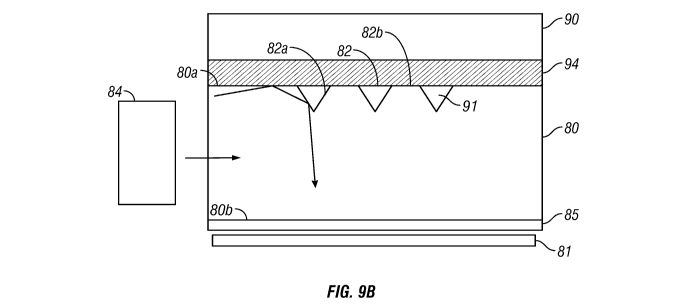
[0073] The turning microstructure 82 and/or light guide region 80 typically
comprises a material such as glass, polycarbonate, acrylic such as
polymethymethacrylate
(PMMA), acrylate copolymers such as poly(styrene-methylmethacrylate) polymers
(PS-
PMMA, sold under the name of Zylar), UV-curable resins, or other optically
transparent
materials. The index of refraction of polycarbonate is approximately 1.59 and
for Zylar is
approximately 1.54 for wavelengths in the visible spectrum. According to some
embodiments, the light guide 80 may be a single layer, such as a plastic or
glass, with facets
formed on the top surface. The facets can be formed, for example, by embossing
or etching
directly onto the plastic or glass substrate. According to other embodiments,
the light guide
80 may include a plurality of layers over a substrate that is glass or
plastic, such as
polycarbonate, PET, etc. In these embodiments, the turning microstructure may
be formed on
a turning film over the substrate, such a UV-embossed resin, or an inorganic
coating etched
to various shapes. The turning film could be chosen to have the same index of
refraction as
the substrate to form one optical body for the light guide 80.
[0074] In other embodiments, one or more additional optical layers, such as an
optical isolation layer may be disposed on the substrate of the display panel
81, or display
elements or interferometric modulators, to otherwise improve the optical
performance of the
display. For example, an optical isolation layer 85 may be provided between
the light
guiding portion 80 of the display and the interferometric modulators 81 to
prevent the
interferometric modulators from absorbing light propagating through the light
guiding
portion.
CA 02726120 2010-11-26
WO 2009/154957 PCT/US2009/045186
[0075] For example, the interferometric modulators are typically absorptive
structures for light rays guided at an angle of 45-90 degrees measured from
the normal to the
display elements. Thus, some of the light propagating through the light guide
80 and incident
on the interferometric modulators 81 at an oblique angle may be substantially
absorbed by the
interferometric modulators 81 after a sufficient number of reflections. In
order to reduce,
minimize, or prevent this loss of light due to absorption, the optical
isolation layer 85 may be
disposed between the light guide region 80 and the interferometric modulators.
According to
some embodiments, the optical isolation layer 85 advantageously has an index
of refraction
substantially lower than the light guide region 80, such that light traveling
through the light
guide 80 and striking the optical isolation film interface at an oblique or
grazing angle, for
example, greater than the critical angle (e.g., greater than 500 or 60 ), will
be totally internally
reflected back into the light guiding region 80. In various embodiments, the
optical isolation
layer 85 comprises silicon dioxide, or fluorinated silicon dioxide. Other
materials may be
employed as well. As described herein, the geometric arrangement of the
turning
microstructure 82, and additional optical films on the substrate relative to
the interferometric
modulators may be selected to enhance the efficiency of the light guiding
portion of the
display, to further enhance the optical performance of the overall display, or
provide other
advantages.
100761 The plurality of display elements 81 may be formed using any of a
variety
of manufacturing processes known to those skilled in the art to adhere one or
more of the
optical layers described herein on the glass or plastic substrate supporting
the array of display
elements. The glass or plastic substrate comprises a support layer upon which
the display
elements, such as an array of interferometric modulators, are fabricated. As
disclosed herein,
the substrate may be further used to support one or more optical layers of the
display device.
[0077] In certain embodiments, the light guide 80 may comprise more than one
layer. For such embodiments, the indices of refraction of the multiple optical
layers
comprising the light guiding portion 80 may in some embodiments advantageously
be close
such that light may be transmitted through the multiple optical layers without
being
substantially reflected or refracted. The light guide 80 may for example have
an index of
21
CA 02726120 2010-11-26
WO 2009/154957 PCT/US2009/045186
refraction of 1.52. As described above, the light guide 80 may comprise glass
or polymeric
material in certain embodiments.
[00781 Figure 9A is a cross-sectional view of a display device as shown in
Figure
8A, but with a cover layer 90 disposed over and attached to the light guide
80, such that the
turning microstructure 82 is under the cover layer 90. The cover layer 90
comprises an
optically transmissive material and is adhered to the light guide 80 such that
a plurality of
regions 91 is preserved between the cover and the plurality of indentations
from turning
features 82a. According to the embodiment shown in Figure 9A, the regions 91
are open
regions, or substantially filled with air. The cover layer 90 protects the
turning
microstructure 82 from the ambient and increases the life of the device by
reducing wear. In
certain embodiments, cover layer 90 may comprise a film stack including other
functionalities, for example, additional layers for anti-glare, anti-
reflection, anti-scratch, anti-
smudge, diffusing, color filtering, or for introducing surface reflections
(e.g., Fresnel
reflections) of ambient light to reduce the display contrast ratio. Cover
layer 90 also makes
possible the easy deposition of the additional layers, since conventional
adhesives used to
laminate the above layers typically contaminate the turning microstructure 82
to the detriment
of optimal performance.
100791 The material of the cover layer 90 facilitates guiding of light within
the
light guide region 80 via total internal reflection. In particular, in various
embodiments the
portion of the cover layer 90 immediately adjacent to the lightguide 80 has an
index of
refraction smaller than that of the light guide 80. Since the index of
refraction of the light
guide 80 is greater than that of cover layer 90, light incident on the
interface of the light guide
80 and the cover layer 90 at an angle greater than the critical angle will be
reflected back into
the light guiding region 80 and will continue to propagate along the light
guiding region 80.
Thus, light that is injected into the edge of light guide 80 is propagated
along its length at
least in part through total internal reflection due to the difference in index
of refraction
between the light guide 80 and the cover layer 90.
100801 In various embodiments, the cover layer 90 is adhered to the light
guide 80
such that the turning microstructure 82 is between the cover layer 90 and the
light guide 80.
The cover layer 90 may be adhered, laminated, pressed, fused etc., onto the
light guide 80, or
22
CA 02726120 2010-11-26
WO 2009/154957 PCT/US2009/045186
another layer between the cover layer 90 and the light guide 80, in a variety
of ways. In
certain embodiments of the invention, cover layer 90 is adhered to light guide
80 such that
the plurality of open regions 91 is preserved. According to some embodiments,
the open
regions 91 are substantially filled with air and provide a difference in
refractive index from
the light guide 80 such that much of the light incident on the turning
features 82a is turned
and redirected towards the plurality of display elements 85. The interface
between the light
guide material and air provides total internal reflection for light incident
on the interface at
angles greater than the critical angle.
[0081] In some embodiments, the cover layer 90 may make direct contact with
the
light guide 80, and in particular embodiments, the cover layer 90 may make
contact for over
about 90% or more of the surface area of the first side 80a of the light guide
80, for example,
on the elevated surfaces 82b of the light guide 80 between the facets 82a. In
other
embodiments, the cover layer 90 does not directly contact the light guide 80
but is attached
by an intervening adhesive layer.
[0082] In some embodiments in which the cover layer 90 directly contacts the
light guide 80, adhesion can be performed by ultrasonic or thermal bonding
between the
surface of cover layer 90 and the elevated surfaces 82b of light guide 80. In
the case of
thermal bonding, which involves the use of heat to bond two surfaces together,
the surface of
the light guide 80 and/or turning microstructure 82 can comprise cross-linked
polymers and
can initially be cured with UV light. The turning microstructure 82 may first
be formed by
UV-embossing, which typically involves replicating from a mold UV-curable
epoxy on a
substrate. This process of UV-embossing the turning microstructure 82 prior to
adhering a
cover film 90 to the elevated surfaces 82b of the microstructure 82 can
prevent or reduce the
likelihood that the surfaces of the light guide 80 and/or turning
microstructure 82 melts
during thermal bonding, and can thus help maintain their shape and light
turning optical
function.
[0083] According to another embodiment, the cover layer 90 may be directly
adhered to light guide 80 by a preparation process that includes activating
either the surface
of cover film 90 or the surfaces of light guide 80 (e.g. turning
microstructure 82), or both,
with a plasma to improve adhesion, and subsequent UV radiation. For example,
an oxygen
23
CA 02726120 2010-11-26
WO 2009/154957 PCT/US2009/045186
plasma can be used to prepare the polymer surface, by first removing weak
surface layers
with the lowest molecular weight, while oxidizing the uppermost atomic layers
of the
polymer. UV radiation can be applied to promote formation of oxygen radicals,
which can
help break bonds and promote the cross linking of surface molecules. The
consequent
oxidation of the polymer causes an increase in polar groups, which enhances
adhesion
properties of the two polymer surfaces during the actual bonding step.
[0084] Figure 9B shows an embodiment of a display device that includes a cover
layer 90 attached to light guide 80 by an adhesive or interlayer 94 between
the cover layer 90
and the turning microstructure 82. According to some embodiments, the
interlayer 94 has an
index of refraction that is smaller than that of the light guide 80 and can
accordingly provide
for total internal reflection of light within the light guide 80. Thus, use of
such an interlayer
94 can advantageously increase material choices by eliminating restrictions on
the index of
refraction for the cover layer 90. Accordingly, the layer directly over
interlayer 94 can be
flexibly chosen for a desired functionality, e.g., for anti-glare, anti-
reflection, color filtering,
etc., regardless of its index of refraction. In some embodiments, the
interlayer is very thin,
e.g., less than 1/10 the size of the depth of feature or indentation of
turning microstructure 82.
Values outside these ranges are also possible. Figure 9C shows an embodiment
of a display
device that includes a cover layer 90 attached to light guide 80 by an
interlayer 94, except that
turning microstructure 83 comprises binary gratings 92. The binary gratings 92
typically
cover large areas so that they can diffract guided light outside the light
guide 80. In some
embodiments, the binary gratings provide open regions.
[0085] According to certain embodiments, the interlayer 94 has very low
surface
energy. For example, interlayer 94 can be a self-wetting adhesive. According
to some
embodiments, the interlayer 94 can have a surface tension of less than 35
dynes/cm.
According to other embodiments, the interlayer 94 can have a surface tension
of less than 25
dynes/cm. A self-wetting interlayer 94 can be applied or coated over a surface
of the cover
layer 90, and the cover layer 90 with the self-wetting interlayer 94 can be
placed over the
light guide 80 and turning microstructure 82. Simple pressure can be applied
over the cover
layer 90 to bond the surface of the interlayer 94 and surface of the light
guide 80, due to the
low surface energy of the interlayer. In some cases, a support frame placed
over the cover
24
CA 02726120 2010-11-26
WO 2009/154957 PCT/US2009/045186
layer 90 and the light guide 80 may be useful to provide the pressure for self-
wetting to
occur.
[0086] According to certain embodiments, the interlayer 94 is a polymer
material
with a low glass transition point (Tg) that is elastically deformable, such as
a rubber or
elastomeric gel-like material. The elastomeric properties can preserve the
regions within the
grooves 82a of the turning microstructure 82 by providing for reversal of any
material ingress
into the grooves 82a when the external force causing initial deformation is
removed. In other
words, the interlayer 94 is sufficiently elastically deformable as to avoid
plastic flow into the
grooves 82a upon external pressure, e.g., from accidental impact during device
operation, that
would prevent total internal reflection. The amount of cross linking could be
increased to
strengthen or rigidify the polymer, where desired, and render it less
sensitive to temperature
changes. According to certain embodiments, the polymer material comprises an
elastomer
material, such as silicone, polypropylene, or poly-isobutylene. According to
certain
embodiments, the interlayer comprises a siloxane backbone, including but not
limited to
polydimethyl siloxane, polydiethyl siloxane, polymethylphenyl siloxane, etc.
According to
some embodiments, the interlayer comprises a silicone elastomer. According to
some
embodiments, the interlayer comprises fluoropolymers, polypropylene and other
amorphous
hydrocarbon polymers with low surface energy to provide an optical bond with
the light
guide, and a refractive index lower than that of the rest of the light guide.
[0087] According to certain embodiments, the interlayer can comprises a
polymer
material with a Tg that is lower than most operating temperatures and
maintains its adhesive
or elastomeric properties under most environmental conditions. For example,
the low Tg
material can have a Tg that is lower than 25 C, 0 C, 20 C,-40 C, etc.
According to certain
embodiments, the polymer material has a glass transition temperature below
about 300 C.
According to other embodiments, the polymer material has a glass transition
temperature
below about 200 C. According to other embodiments, the polymer material has a
glass
transition temperature below about 0 C.
[0088] According to some embodiments, the interlayer has an index of
refraction
that is sufficiently lower than that of the light guide to provide for total
internal reflection.
According to some embodiments, the interlayer has a sufficiently low surface
energy to
CA 02726120 2010-11-26
WO 2009/154957 PCT/US2009/045186
physically couple the cover to areas of the turning microstructure between the
grooves.
According to some embodiments, the interlayer has sufficiently elastomeric
properties to
preserve open regions in the turning microstructure and preserve total
internal reflection. In
some embodiments, the interlayer does not fill at least 50%, 60%, 70%, 80%, or
90% of the
grooves, indentations or turning microstructure disposed across the light
guide. Additionally,
according to some embodiments, the interlayer does not fill substantially all
of the region
within the groove of the turning microstructure. For example, according to
some
embodiments, on average, the interlayer does not fill at least 50%, 60%, 70%,
80%, or 90%
of the region within the grooves or turning microstructure. According to some
embodiments,
the interlayer has an index of refraction that is sufficiently lower than that
of the light guide
to provide for total internal reflection, a sufficiently low surface energy to
physically couple
the cover to areas of the turning microstructure between the grooves, and
sufficiently
elastomeric properties to preserve open regions in the turning microstructure
and preserve
total internal reflection.
[0089] According to certain embodiments, the thickness of the interlayer 94 is
less than the height of the indentation of the turning microstructure.
According to certain
embodiments, the thickness of the interlayer 94 is less than 1/2, 1/4, 1/8,
1/10, etc., the height
of the indentations. For example, if an indentation of the turning
microstructure is about 2
microns tall, the interlayer thickness can be about 200 nm thick. According to
some
embodiments, the thickness of the interlayer 94 can be 10 microns or more, 20
microns or
more, 50 microns or more, or 100 microns or more.
[0090] Such an adhesive layer can be formed by conventional wet coating
processes, such as spin, spray, dip, roll, inkjet, etc., which can typically
form very thin films
by employing dilute solutions of the coating material. After a very thin
adhesive layer is
formed on cover layer 90, the cover layer 90 with the thin adhesive can be
placed over the
light guide 80 with the application of pressure and temperature to provide
contact with
surfaces 82b of turning microstructure 82. The thin adhesive can then be cured
with UV light
or heat to bond the surface of cover layer 90 with surfaces of the turning
microstructure 82.
[0091] In various embodiments, the films are made to be very thin to reduce or
minimize the risk of excess adhesive material filling the grooves of the
turning
26
CA 02726120 2010-11-26
WO 2009/154957 PCT/US2009/045186
microstructure 82 after lamination of the adhesive material on the cover layer
90. Reducing
or minimizing thickness of the adhesive material would keep the regions 91
within the
grooves or indentations 82a open, and the optical performance of the display
device
optimized. Light over a wider range of angle total internally reflects if air
having an index of
1.0 is within the indentation. Moreover, even if the filling of some adhesive
material in the
grooves 82a of the turning microstructure 82 occurs, the size of the grooves
and amount of
adhesive material can be configured such that the amount of adhesive material
that falls into
the grooves 82a may reduce the size of the open regions 91, without entirely
filling the
regions. Partial filling of the grooves 82a may decrease the likelihood that
the grooves are
visible to a viewer and/or may be factored into the design of the illumination
system (e.g., in
the selection of groove width).
[00921 For the embodiment of a very thin adhesive film, it can be advantageous
that the adhesive material shows sufficient mechanical compliance so that
optical contact can
be increased or maximized. According to some embodiments, the adhesive
material
comprises a polymer material having a low glass transition point and is thus
gel-like and
deformable, but also having a high viscosity, or highly cross-linked networks.
Preferably, the
adhesive material comprises a soft polymer material that can conform easily to
another
surface, particularly a surface that has been UV-cured and is less compliant,
and thus the
adhesive material has a low molecular weight in various embodiments. Examples
include
acrylic pre-polymer mixtures, which have high viscosities, including for
example
polymethymethacrylate (PMMA), and poly(styrene-methylmethacrylate) (PS-PMMA),
and
other acrylic polymers. Other examples include polymer formulations typically
used as
pressure sensitive adhesives.
100931 According to some embodiments, the index of refraction of the adhesive
layer 94, which directly overlies the turning microstructure 83, has a lower
index of refraction
than that of the light guide 80 so that total internal reflection can occur
within the light guide
80.
[00941 According to certain embodiments of a thicker adhesive, the thickness
can
be equal to or larger than the size of a feature 82a in the turning
microstructure 82, and can
range for example, from about .5 micron to about 50 microns in thickness.
Since there is
27
CA 02726120 2010-11-26
WO 2009/154957 PCT/US2009/045186
enough adhesive material to fill the grooves of the turning microstructure in
this case, the
adhesive material may be cured such that it does not flow or plastically
deform when
attaching the cover 90 to the light guide 80, in order to avoid the filling of
grooves 82a with
adhesive material during lamination. The process of forming a thicker adhesive
is similar to
the process of forming a thin adhesive as set forth above. However, the
adhesive mixture in
the embodiment of the thicker adhesive can be additionally cured to further
reduce or
minimize the flowability of the thick adhesive material. According to some
embodiments, a
thick adhesive material, such as a polymer material, is first coated onto or
deposited over a
cover layer 90. The thick adhesive material can be pre-cured to partially
cross-link the
polymer chains, and stop the flow of the adhesive. The cover layer with the
thick adhesive
can then be placed over the light guide panel 80 with the application of
pressure and
temperature to provide optical contact. The thick adhesive can then be cured a
second time
with UV light or heat to complete partial cross-linking and seal the surface
of cover layer 90
with surfaces of the light guide 80. The pre-curing step helps avoid the
filling or partial
filling of grooves 82a of the turning microstructrure 82 with the thick
adhesive material.
[0095] According to some embodiments, the adhesive materials comprise
polymer materials with low glass transition points, highly cross-linked
networked materials,
or gel-like structures. According to some embodiments, the adhesive materials
comprise
silicones such as polydimethyl siloxanes, polydiethyl siloxanes,
polymethylphenyl siloxanes,
or acrylates with hydrocarbon side chains, such as t-butyl acrylate, or
polyester materials,
such as polytetramethylene ether glycol. Some embodiments provide the
opportunity to
further cross-link and fortify the adhesive, such as by including additional
cross-linking
density. As discussed above, the index of refraction of the thicker adhesive
layer is lower
than that of the light guide 80 in some embodiments. Moreover, the thicker
adhesive can
provide additional functionalities, such as optical diffusion, color
filtering, mechanical shock
absorption, etc.
[0096] According to another embodiment, the cover layer 90 can be solvent-
welded, which includes exposing a surface of a cover layer 90 to a solvent
that is chemically
soluble with the surfaces of the cover layer 90 and of the light guide 80. The
cover layer 90
with the solvent applied over a surface may be placed over the light guide 80.
In some
28
CA 02726120 2010-11-26
WO 2009/154957 PCT/US2009/045186
embodiments, application of pressure and temperature can increase optical
contact and
provides for inter-diffusion between the surface of the cover layer 90 and
surfaces in areas
82b between the grooves. In certain embodiments, the light guide 80 can
comprise a material
that is cross-linked and UV-cured so that the solvent does not dissolve the
features 82a of the
turning microstructure 82.
[0097] According to various embodiments, the solvent comprises a liquid
solvent.
According to certain embodiments, the solvent comprises a polymerizable
mixture. The
polymerizable mixture may comprise a monomer and an initiator, unless the
monomer itself
can self-initiate. According to some embodiments, a solvent may further
comprise molecular
coupling agents, including tri-functional amino silanes (e.g., amino propyl
tri-ethoxy silane),
which activates the surfaces for bonding during lamination of the cover layer
90 to the light
guide 80 and improves the seal between surfaces. An advantage of adding a
molecular
coupling agent, such as certain amino silanes, to a solvent applied to a cover
layer 90 is that
the amino groups of the molecular coupling agent, such as NH2 groups, can more
easily react
with the material of the light guide 80. For example, a silane-based coupling
agent may bond
readily with surface hydroxyl groups of the light guide 80, and render the
surface of the light
guide 80 more active towards bonding with cover layer 90. Other coupling
agents as known
in the art, including various silicates and titanates, can accordingly be used
to increase the
interfacial bonds between the surfaces of the cover and the light guide 80.
[0098] According to certain embodiments, the open regions 82a can be filled
with
air. However, according to other embodiments as shown in Figure 1 OA, the
regions 82a may
be filled with a material to form filled regions 95. In some embodiments, the
material may
comprise a substantially porous material, or may comprise a material with an
index of
refraction that is substantially close to that of air so that light would be
similarly directed by
total internal reflection. According to another embodiment, the material may
comprise a
metallic material which acts as a mirror reflector and reduces or minimizes
the need to trap
air pockets between the light guide 80 and cover layer 90. Suitable deposition
methods for
the metallic material include direct vacuum coating followed by patterning
using techniques
known in the microfabrication field (e.g., photolithography followed by
etching of excess
metal layer, or lift-off techniques), or localized deposition such as by
inkjet printing. While
29
CA 02726120 2010-11-26
WO 2009/154957 PCT/US2009/045186
inkjet printing provides the advantage of achieving a line width as small as
about 15 microns,
other printing or deposition technologies may be used.
[0099] According to some embodiments, as shown in Figure 10B, the grooves
82a are not filled with a material, and the adhesive layer 94 is coated to
produce a particular
desired spatial arrangement, for example by inkjet printing, such that after
the cover layer 90
and the lightguide 80 are bonded, the adhesive 94 will not flow into the
grooves and thus
preserve open regions 91. According to another embodiment shown in Figure IOC,
protruding structures 98 may be UV-embossed areas immediately adjacent to and
separating
the grooves 82a, to prevent adhesive material from entering the grooves during
the
lamination process and help preserve open regions 91. According to certain
embodiments as
shown in Figures I OB and IOC, the open regions 91 extend from the grooves 82a
to the lower
surface of cover layer 90.
[0100] According to another embodiment (not shown), the turning microstructure
can comprise binary gratings as shown in FIG. 9C, but that are also filled. By
inkjet printing
a low refractive index material such as fluoroplastic, aerogel, sol-gel, etc.,
in the diffractive
regions, and by maintaining the difference in refractive index constant
between the light
guide and the low index coating material, diffraction efficiency can be
increased or
optimized.
[0101] The turning microstructures according to some embodiments can be
formed by the process shown in Figure 11. First, a dissolvable layer 97, such
as photoresist,
can be formed over the first side of the light guide 80. A plurality of
grooves or indentations
82a can then be formed through the dissolvable layer 97 and into the first
side of the light
guide 80. A reflective material 99 can then be formed over the dissolvable
layer 97 and light
guide 80 so that the material fills the indentations 82a and lies over the
dissolvable layer 97
in areas 82b between grooves 82a. According to some embodiments, reflective
material 99
can be a layer of aluminum, silver, or other metals. According to some
embodiments, the
thickness of reflective material 99 is at least 50 nm. According to other
embodiments, the
thickness of reflective material 99 is at least 100 nm. Next, the dissolvable
layer 97 is
removed so that the overlying metal is also lifted off in areas 82b between
the grooves 82a.
According to some embodiments, the groove 82a can be lined or only partially
filled with
CA 02726120 2010-11-26
WO 2009/154957 PCT/US2009/045186
reflective material 99. That is, the reflective material 99 need not
completely fill the groove
82a to provide reflection. Consequently, an overlying adhesive material need
not be an
elastomeric or elastically deformable material. As shown in the last block of
Figure 11, the
space within the groove over the lining of reflective material 99 may be
filled with material
from an overlying interlayer 94. According to the illustrated embodiment, the
space above
the reflective material 99 need not be kept open because reflection would be
preserved from
the reflective material lining of the grooves. For this reason, the space
within the grooves can
also be completely filled with reflective material 99 according to other
embodiments.
According to other embodiments, groove 82a can first be lined or partially
filled with
reflective material 99, and additional planarizing steps can be subsequently
taken to form a
microstructure such that the grooves 82a are completely filled with the
reflective material 99
(not shown).
[01021 A wide variety of variations are possible. Films, layers, components,
and/or elements may be added, removed, or rearranged. Additionally, processing
steps may
be added, removed, or reordered. Also, although the terms "film" and "layer"
have been used
herein, such terms as used herein may include film stacks and multilayers.
Such film stacks
and multilayers may be adhered to other structures using adhesive or may be
formed on other
structures using deposition or in other manners.
[01031 Moreover, although this invention has been disclosed in the context of
certain preferred embodiments and examples, it will be understood by those
skilled in the art
that the present invention extends beyond the specifically disclosed
embodiments to other
alternative embodiments and/or uses of the invention and obvious modifications
and
equivalents thereof. In addition, while several variations of the invention
have been shown
and described in detail, other modifications, which are within the scope of
this invention, will
be readily apparent to those of skill in the art based upon this disclosure.
It is also
contemplated that various combinations or sub-combinations of the specific
features and
aspects of the embodiments may be made and still fall within the scope of the
invention. It
should be understood that various features and aspects of the disclosed
embodiments can be
combined with, or substituted for, one another in order to form varying modes
of the
disclosed invention. Thus, it is intended that the scope of the present
invention herein
31
CA 02726120 2010-11-26
WO 2009/154957 PCT/US2009/045186
disclosed should not be limited by the particular disclosed embodiments
described above, but
should be determined only by a fair reading of the claims that follow.
32