Note: Descriptions are shown in the official language in which they were submitted.
CA 02737251 2011-03-14
WO 2010/028490 PCT/CA2009/001261
TOUCH INPUT WITH IMAGE SENSOR AND SIGNAL PROCESSOR
Cross-Reference To Related Applications
[0001] This application is a continuation-in-part of U.S. Patent Application
No. 12/118,545 to Hansen et al. filed on May 9, 2008 and entitled "Interactive
Input
System and Bezel Therefor", the content of which is incorporated herein by
reference.
This application also claims the benefit of U.S. Provisional Application No.
61/097,206 to McGibney et al. filed on September 15, 2008 entitled
"Interactive Input
System", the content of which is incorporated herein by reference.
Field Of The Invention
[0002] The present invention relates to an interactive input system.
Background Of The Invention
[0003] Interactive input systems that allow users to inject input (eg. digital
ink, mouse events etc.) into an application program using an active pointer
(eg. a
pointer that emits light, sound or other signal), a passive pointer (eg. a
finger, cylinder
or other object) or other suitable input device such as for example, a mouse
or
trackball, are well known. These interactive input systems include but are not
limited
to: touch systems comprising touch panels employing analog resistive or
machine
vision technology to register pointer input such as those disclosed in U.S.
Patent Nos.
5,448,263; 6,141,000; 6,337,681; 6,747,636; 6,803,906; 7,232,986; 7,236,162;
and
7,274,356 assigned to SMART Technologies ULC of Calgary, Alberta, Canada,
assignee of the subject application, the contents of which are incorporated by
reference; touch systems comprising touch panels employing electromagnetic,
capacitive, acoustic or other technologies to register pointer input; tablet
personal
computers (PCs); laptop PCs; personal digital assistants (PDAs); and other
similar
devices.
[0004] Above-incorporated U.S. Patent No. 6,803,906 to Morrison et al.
discloses a touch system that employs machine vision to detect pointer
interaction
with a touch surface on which a computer-generated image is presented. A
rectangular bezel or frame surrounds the touch surface and supports digital
cameras at
SUBSTITUTE SHEET (RULE 26)
CA 02737251 2011-03-14
WO 2010/028490 PCT/CA2009/001261
-2-
its corners. The digital cameras have overlapping fields of view that
encompass and
look generally across the touch surface. The digital cameras acquire images
looking
across the touch surface from different vantages and generate image data.
Image data
acquired by the digital cameras is processed by on-board digital signal
processors to
determine if a pointer exists in the captured image data. When it is
determined that a
pointer exists in the captured image data, the digital signal processors
convey pointer
characteristic data to a master controller, which in turn processes the
pointer
characteristic data to determine the location of the pointer in (x,y)
coordinates relative
to the touch surface using triangulation. The pointer coordinates are conveyed
to a
computer executing one or more application programs. The computer uses the
pointer
coordinates to update the computer-generated image that is presented on the
touch
surface. Pointer contacts on the touch surface can therefore be recorded as
writing or
drawing or used to control execution of application programs executed by the
computer.
[00051 U.S. Patent Application Publication No. 2004/0179001 to Morrison et
al. discloses a touch system and method that differentiates between passive
pointers
used to contact a touch surface so that pointer position data generated in
response to a
pointer contact with the touch surface can be processed in accordance with the
type of
pointer used to contact the touch surface. The touch system comprises a touch
surface
to be contacted by a passive pointer and at least one imaging device having a
field of
view looking generally along the touch surface. At least one processor
communicates
with the at least one imaging device and analyzes images acquired by the at
least one
imaging device to determine the type of pointer used to contact the touch
surface and
the location on the touch surface where pointer contact is made. The
determined type
of pointer and the location on the touch surface where the pointer contact is
made are
used by a computer to control execution of an application program executed by
the
computer.
[00061 Although many different types of interactive input systems exist,
improvements to such interactive input systems are continually being sought.
It is
therefore an object of the present invention to provide a novel interactive
input
system.
SUBSTITUTE SHEET (RULE 26)
CA 02737251 2011-03-14
WO 2010/028490 PCT/CA2009/001261
-3-
Summary Of The Invention
[0007] Accordingly, in one aspect there is provided an interactive input
system comprising at least two imaging assemblies capturing image frames of a
region of interest from different vantages; and processing structure
processing image
frames captured by said imaging assemblies to determine the location of a
pointer
within the region of interest, wherein each imaging assembly comprises an
image
sensor and integrated signal processing circuitry.
[0008] According to another aspect there is provided an interactive input
system comprising at least one imaging device having a field of view looking
into a
region of interest; and at least one radiation source emitting radiation into
said region
of interest, wherein during image frame capture by said at least one imaging
device,
the operation of the at least one radiation source is synchronized with the
exposure
time of said at least one imaging device
Brief Description Of The Drawings
[0009] Embodiments will now be described more fully with reference to the
accompanying drawings in which:
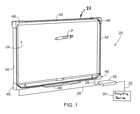
[0010] Figure 1 is a perspective view of an interactive input system;
[0011] Figure 2 is a block diagram view of the interactive input system of
Figure 1;
[0012] Figure 3 is a perspective conceptual view of a portion of the
interactive
input system of Figure 1;
[0013] Figure 4A is a block diagram of an image sensor and associated signal
processing circuitry forming part of the interactive input system of Figure 1;
[0014] Figure 4B is a block diagram of another embodiment of the image
sensor and associated signal processing circuitry for the interactive input
system of
Figure 1;
[0015] Figure 5 is another schematic diagram block diagram of the image
sensor and associated signal processing circuitry of Figure 4A;
SUBSTITUTE SHEET (RULE 26)
CA 02737251 2011-03-14
WO 2010/028490 PCT/CA2009/001261
-4-
[0016] Figures 6A and 6B are block diagrams of further alternative image
sensors and associated signal processing circuitry for the interactive input
system of
Figure 1; and
[0017] Figures 7A and 7B are block diagrams of still further alternative image
sensors and associated signal processing circuitry for the interactive input
system of
Figure 1.
Detailed Description Of The Embodiments
[0018] Turning now to Figures 1 to 3, an interactive input system that allows
a
user to inject input (eg. digital ink, mouse events etc.) into an application
program is
shown and is generally identified by reference numeral 20. In this embodiment,
interactive input system 20 comprises an assembly 22 that engages a display
unit (not
shown) such as for example, a plasma television, a liquid crystal display
(LCD)
device, a flat panel display device, a cathode ray tube etc. and surrounds the
display
surface 24 of the display unit. The assembly 22 employs machine vision to
detect
pointers brought into a region of interest in proximity with the display
surface 24 and
communicates with a central hub 26 via communication lines 28. The
communication
lines 28 in this embodiment are embodied in a serial bus.
[0019] The central hub 26 also communicates with a general purpose
computing device 30 executing one or more application programs via a USB cable
32.
Computing device 30 comprises for example a processing unit, system memory
(volatile and/or non-volatile), other non-removable or removable memory (a
hard disk
drive, RAM, ROM, EEPROM, CD-ROM, DVD, flash memory etc.) and a system bus
coupling the various computing device components to the processing unit. The
computing device 30 processes the image data output of the assembly 22
received via
the central hub 26 and adjusts image data that is output to the display unit
so that the
image presented on the display surface 24 reflects pointer activity. In this
manner, the
assembly 22, central hub 26 and computing device 30 allow pointer activity
proximate to the display surface 24 and within the region of interest to be
recorded as
writing or drawing or used to control execution of one or more application
programs
executed by the computing device 30.
SUBSTITUTE SHEET (RULE 26)
CA 02737251 2011-03-14
WO 2010/028490 PCT/CA2009/001261
-5-
[0020] Assembly 22 comprises a frame assembly that is mechanically
attached to the display unit and surrounds the display surface 24. Frame
assembly
comprises a bezel having three bezel segments 40, 42 and 44, four corner
pieces 46
and a tool tray segment 48. Bezel segments 40 and 42 extend along opposite
side
edges of the display surface 24 while bezel segment 44 extends along the top
edge of
the display surface 24. The tool tray segment 48 extends along the bottom edge
of the
display surface 24 and supports one or more pen tools P. The corner pieces 46
adjacent the top left and top right corners of the display surface 24 couple
the bezel
segments 40 and 42 to the bezel segment 44. The corner pieces 46 adjacent the
bottom left and bottom right corners of the display surface 24 couple the
bezel
segments 40 and 42 to the tool tray segment 48. In this embodiment, the corner
pieces 46 adjacent the bottom left and bottom right corners of the display
surface 24
also accommodate imaging assemblies 60 that look generally across the entire
display
surface 24 from different vantages. The bezel segments 40, 42 and 44 are
oriented so
that their inwardly facing surfaces are seen by the imaging assemblies 60.
[0021] In this embodiment, the inwardly facing surface of each bezel segment
40, 42, 44 comprises a single strip or band of retro-reflective material. To
take best
advantage of the properties of the retro-reflective material, the bezel
segments 40, 42
and 44 are oriented so that their inwardly facing surfaces lie in planes that
are
generally normal to the plane of the display surface 24. Alternatively, the
bezel
segments 40, 42 and 44 may be of the type disclosed in above-incorporated U.S.
Patent Application Serial No. 12/118,545 to Hansen et al.
[0022] Turning now to Figures 4A and 5, one of the imaging assemblies 60 is
better illustrated. As can be seen, each imaging assembly 60 comprises an
image
sensor 70 that communicates with signal processing circuitry 72. In this
embodiment,
the image sensor 70 of each imaging assembly 60 is of the type manufactured by
Micron under model No. MT9V023 and is fitted with an 880nm lens of the type
manufactured by Boowon under model No. BW25B giving the image sensor 70 a
field of view greater than ninety (90) degrees. Of course, those of skill in
the art will
appreciate that other commercial or custom image sensors may be employed.
[0023] In this embodiment, the signal processing circuitry 72 is implemented
on an integrated circuit such as for example a field programmable gate array
(FPGA)
SUBSTITUTE SHEET (RULE 26)
CA 02737251 2011-03-14
WO 2010/028490 PCT/CA2009/001261
-6-
chip and is assembled on a printed circuit board with the image sensor 70 as
shown in
Figure 4A. Alternatively, the image sensor 70 and the signal processing
circuitry 72
may be fabricated on a single integrated circuit die 102 as shown in Figure
4B. The
signal processing circuitry 72 comprises a sensor interface 80 that provides
image
data to a bezel processor 82, and to a spotlight processor 84. The sensor
interface 80
also provides synchronization information to a lighting controller 88 and to
an output
buffer 90. The output buffer 90 is coupled to a serial interface 92 which
itself is
coupled to the clock and data lines 92a and 92b, respectively, of the serial
bus 28.
The sensor interface 80 includes an 12 C bus interface 80a that controls the
transmission of data between the image sensor 70 and the signal processing
circuitry
72. All input/output and clock lines of the image sensor 70 are wired directly
to the
signal processing circuitry 72 so that no support hardware is required. Data
coming
through the serial interface 92 that is addressed to the image sensor 70 is
reformatted
by the I2C bus interface 80a and sent directly to the image sensor 70.
[0024] The signal processing circuitry 72 also comprises 4 Mbits of flash
memory 94, a bezel file 96 and control registers 98. The flash memory 94
contains
sufficient space for two FPGA chip configuration files and about 1 Mbit for
user
information. One configuration file is used to reprogram the FPGA chip for a
fail safe
or factory diagnostics mode. The user information memory is used to store
image
sensor parameters, serial numbers and other information relevant to the image
sensor.
[0025] The lighting controller 88 is connected to a radiation source such as
an
infrared (IR) light source 100 comprising a plurality of IR light emitting
diodes
(LEDs) and associated lens assemblies. The total power for the IR light source
100 in
this embodiment is 300mW. The IR light source 100 is only turned on during the
exposure times of the image sensor 70, resulting in a duty cycle of
approximately 8%
and an average power draw of approximately 25mW. The control signals for the
IR
light source 100 are supplied by the lighting controller 88 in response to
synchronization signal output from the image sensor 70 that is received by the
lighting controller 88 via the sensor interface 80.
[0026] The FPGA chip in this embodiment comprises a security system that
includes a unique identifier for the FPGA chip (64 bytes) and a one-time
programmable security register (64 bytes). The security register can be
programmed
SUBSTITUTE SHEET (RULE 26)
CA 02737251 2011-03-14
WO 2010/028490 PCT/CA2009/001261
-7-
in the factory with a unique code that unlocks the FPGA chip. Any attempt to
copy a
configuration file from one FPGA chip to another FPGA chip causes the FPGA
chip
to shut down. The FPGA chip also includes multiple on-chip or internal clocks.
The
clock of the image sensor 70 and all FPGA internal clocks are synthesized from
clock
input received by the serial interface 92 via the clock line 92a of the serial
bus 28
without an external crystal. Generating the high-frequency clocks locally on
the
imaging assembly 60 helps to reduce electromagnetic interference (EMI). The
FPGA
chip in this embodiment also comprises approximately 200,000 gates, 288Kbits
of on
chip static memory, and 195 1/O pins. For example, the Xilinx XC3S200AN FPGA
chip could be used. The static memory is allocated as follows. The bezel file
96 uses
16 kbit of static memory, the internal register of the bezel processor 92 uses
16 kbit of
static memory, the internal register of the spotlight processor 84 uses 16
kbit of static
memory, and the output buffer 90, which is double buffered, uses 32kbit of
static
memory.
[0027] The signal processing circuitry 72 serves multiple purposes. The
primary function of the signal processing circuitry 72 is to perform pre-
processing on
the image data generated by the image sensor 70 and stream the results to the
central
hub 26. The signal processing circuitry 72 also performs other functions
including
control of the IR light source 100, lens assembly parameter storage, anti-copy
security
protection, clock generation, serial interface, and image sensor
synchronization and
control.
[0028] The central hub 26 comprises a universal serial bus (USB) micro-
controller that is used to maintain the serial links to the imaging assemblies
60,
package the image information received from the imaging assemblies 60 into USB
packets, and send the USB packets over the USB cable 32 to the computing
device 30
for further processing.
[0029] Communications between the central hub 26 and the imaging
assemblies 60 over the serial bus 28 is bidirectional and is carried out
synchronously
at a rate of 2 Mbit/s in each direction. The communication rate may be
increased to
reduce latency if desired. The clock and data lines 92a and 92b, respectively,
of the
serial bus 28 carry a differential pair of clock and data signals. The clock
line 92a is
driven from the central hub 26 and serves the dual purpose of serially
clocking image
SUBSTITUTE SHEET (RULE 26)
CA 02737251 2011-03-14
WO 2010/028490 PCT/CA2009/001261
-8-
data and providing a reference clock for the imaging assemblies 60. When data
is on
the data line 92b of the serial bus 28, the clock and data lines 92a and 92b
are driven
by the central hub 26 in opposite polarity. When the serial bus 28 is
released, pull-up
resistors (not shown) pull both the clock and data lines high. The central hub
26 pulls
both the clock and data lines low simultaneously to reset the imaging
assemblies 60.
The central hub 26 is therefore able to reset and release all the printed
circuit boards
together to synchronize the imaging assemblies 60. The serial bus 28 is in the
form of
a ribbon cable for short distances and a cat-5 cable for longer distances.
100301 The central hub 26 also comprises a switching voltage regulator to
provide an input 3.3V logic supply voltage to each imaging assembly 60 that is
used
to power the image sensors 70. A 1.2V logic supply voltage for the FPGA chip
is
generated from the 3.3V logic supply voltage in each imaging assembly 60 by a
single
linear voltage regulator (not shown). External current regulators, storage
capacitors,
and switching capacitors for running the IR light sources 100 are also
contained in the
central hub 26. The switching voltage regulator to run the IR light sources
100 is
approximately 0.5V above the LED forward bias voltage.
[00311 The interactive input system 20 is designed to detect a passive pointer
such as for example, a user's finger F, a cylinder or other suitable object
that is
brought into proximity with the display surface 24 and within the fields of
view of the
imaging assemblies 60.
[00321 The general operation of the interactive input system 20 will now be
described. Each imaging assembly 60 acquires image frames looking generally
across
the display surface 24 within the field of view of its image sensor 60 at the
frame rate
established by the signal processing circuitry clock signals. When the IR
light sources
100 are on, the LEDs of the IR light sources flood the region of interest over
the
display surface 24 with infrared illumination. Infrared illumination that
impinges on
the retro-reflective bands of the bezel segments 40, 42 and 44 is returned to
the
imaging assemblies 60. As a result, in the absence of a pointer, each imaging
assembly 60 sees a bright band having a substantially even intensity over its
length.
When a pointer is brought into proximity with the display surface 24, the
pointer
occludes infrared illumination reflected by the retro-reflective bands of the
bezel
segments 40, 42 and 44. As a result, the pointer appears as a dark region that
SUBSTITUTE SHEET (RULE 26)
CA 02737251 2011-03-14
WO 2010/028490 PCT/CA2009/001261
-9-
interrupts the bright band in captured image frames. The signal processing
circuitry
72 processes the image frames to determine if one or more pointers are
captured in the
image frames and if so, to generate pointer data.
[0033] The central hub 26 polls the imaging assemblies 60 at a set frequency
(in this embodiment 120 times per second for an image capture frequency of 960
frames per second (fps)) for pointer data and performs triangulation on the
pointer
data to determine pointer position data. The central hub 26 in turn transmits
pointer
position data and/or image assembly status information to the computing device
30.
In this manner, pointer position data transmitted to the computing device 30
can be
recorded as writing or drawing or can be used to control execution of
application
programs executed by the computing device 30. The computing device 30 also
updates the display output conveyed to the display unit so that the presented
image
reflects the pointer activity. The central hub 26 also receives commands from
the
computing device 30 and responds accordingly as well as generates and conveys
diagnostic information to the imaging assemblies 60.
[0034] Initially, an alignment routine is performed to align the image sensors
70. During the alignment routine, a pointer is held in the approximate center
of the
display surface 24. Following image frame capture, subsets of the pixels of
the image
sensors 70 are then selected until a subset of pixels for each image sensor 70
is found
that captures the pointer and the pointer tip on the display surface 24. This
alignment
routine allows for a relaxation in mechanical mounting of the image sensors
70. The
identification of the pointer tip on the display surface 24 also gives
calibration
information for determining the row of pixels of each image sensor 70 that
corresponds to actual pointer contacts made with the display surface 24.
Knowing
these pixel rows allows the difference between pointer hover and pointer
contact to be
readily determined.
[0035] In this embodiment, since a computing device display is projected onto
the display surface 24, during the alignment routine several known coordinate
locations are also displayed on the display surface 24 and the user is
prompted to
touch these coordinate locations in sequence using the pointer so that the
subset of
pixels for each of image sensor 70 includes all of these touch coordinate
locations as
SUBSTITUTE SHEET (RULE 26)
CA 02737251 2011-03-14
WO 2010/028490 PCT/CA2009/001261
-10-
well. Calibration data is then stored for reference so that pointer contacts
on the
display surface 24 can be mapped to corresponding areas on the computer
display.
[0036] As mentioned above, each imaging assembly 60 acquires image frames
looking generally across the display surface 24 within its field of view. The
image
frames are acquired by the image sensors 70 at intervals in response to the
clock
signals received from the signal processing circuitry 72. The signal
processing
circuitry 72 in turn reads each image frame from the image sensor 70 and
processes
the image frame to determine if a pointer is located in the image frame and if
so,
extracts pointer and related pointer statistical information from the image
frame. To
avoid processing significant numbers of pixels containing no useful
information,
several components of the signal processing circuitry 72 pre-process the image
frame
data as will be described.
[0037] The pointer data generated by the signal processing circuitry 72 of
each imaging assembly 60 is only sent to the central hub 26 when the imaging
assembly 60 is polled by the central hub 26. The signal processing circuitries
72
create pointer data faster than the central hub 26 polls the imaging
assemblies 60.
However, the central hub 26 may poll the imaging assemblies 60 at a rate
synchronous with the creation of the processed image data. Processed image
data that
is not sent to the central hub 26 is overwritten.
[0038] When the central hub 26 polls the imaging assemblies 60, frame sync
pulses are sent to the imaging assemblies 60 to initiate transmission of the
pointer data
created by the signal processing circuitries 72. Upon receipt of a frame sync
pulse,
each signal processing circuitry 72 transmits pointer data to the central hub
26 over
the data lines 92b of the serial bus 28. The pointer data that is received by
the central
hub 26 is auto-buffered into the central hub processor.
[0039] After the central hub processor has received pointer data from each of
the imaging assemblies 60, the central hub processor processes the received
pointer
data to calculate the position of the pointer in (x,y) coordinates relative to
the display
surface 24 using triangulation in a well known manner such as that described
in
above-incorporated U.S. Patent No. 6,803,906 to Morrison et al. The calculated
pointer coordinate is then conveyed to the computing device 30. The computing
device 30 in turn processes the received pointer coordinate and updates the
image
SUBSTITUTE SHEET (RULE 26)
CA 02737251 2011-03-14
WO 2010/028490 PCT/CA2009/001261
-11-
output provided to the display unit, if required, so that the image presented
on the
display surface 24 reflects the pointer activity. In this manner, pointer
interaction
with the display surface 24 can be recorded as writing or drawing or used to
control
execution of one or more application programs running on the computing device
26.
[0040] As mentioned above, several components of the signal processing
circuitry 72 pre-process the image data to create the pointer data. The bezel
processor
82 performs pre-processing steps to improve the efficiency of the interactive
input
system signal processing operations. One of these pre-processing steps is
ambient
light reduction. The image sensors 70 are run at a much higher frame rate than
is
required and the IR light sources 100 are turned on during alternate image
frames.
The bezel processor 82 subtracts image frames captured while the IR light
sources
100 are on from image frames captured while the IR light sources 100 are off.
Ambient light is relatively constant across image frames so the ambient light
is
canceled during this process and does not appear in the difference image
frames. In
this embodiment, the image sensors 70 run at a frame rate 8 times the desired
output
rate. For every eight image frames captured, four image fames are captured
while the
IR light sources 100 are on and four frames are captured while the IR light
sources
100 are off. The four frames captured while the IR light sources 100 are off
are then
subtracted from the four frames captured while the IR light sources 100 are on
and the
resultant difference frames are added to produce one image.
[0041] The bezel processor 82 also performs signal processing operations to
capture and track one or more pointers on the display surface 24. The output
of the
bezel processor 82 is a single number for each column of the image data that
indicates
the presence of a pointer. In this embodiment, the bezel processor 82 performs
continuity calculations to identify the pointer in the image data. The bezel
processor
82 adds a number of pixels in a column in the image data corresponding to a
bright
part of the bezel and then subtracts the same number of pixels from the image
data
corresponding to a dark part just above the bezel. If no pointer is present
then this
will show very high contrast. If a pointer is present, whether bright or dark,
the
lighting will be approximately equal in both regions and the contrast will be
low. The
location of the bezel and the number of points to add/subtract are stored in
the bezel
file 96.
SUBSTITUTE SHEET (RULE 26)
CA 02737251 2011-03-14
WO 2010/028490 PCT/CA2009/001261
-12-
[0042] Error checking is done by the bezel processor 82 regardless of the type
of bezel and pointer used. The bezel processor monitors the image sensor 70 to
determine if a very strong light source has saturated the image sensor. If the
image
sensor is saturated, a flag is set. The flag triggers a warning message to be
displayed
so that a user can take steps to remove or attenuate the very strong light
source.
[0043] While the bezel processor 82 is the main means of capturing and
tracking objects on the display surface 24, the spotlight processor 84 is a
secondary
mechanism that allows regions in the image data that may contain a pointer to
be
extracted. Unlike the bezel processor, the spotlight processor 84 employs
feedback
from the central hub 26. If the feedback is delayed or incorrect, then a
pointer can
still be detected with reduced functionality/accuracy. The spotlight processor
84
employs a movable window, preferably 32x32 pixels or 64x16 pixels that is
extracted
from the image data and sent back to the central hub 26 after light processing
and
zooming. The central hub 26 can select several lighting modes for the
spotlight that
are independent of the bezel processor 82. These lighting modes include
ambient
light rejection, bezel light rejection, and normal exposure (ambient and bezel
light).
The central hub 26 can also specify that the spotlight be zoomed out to view
larger
targets. For example, to capture a target that is 150 pixels wide the central
hub
specifies that the image be zoomed out by a factor of 4 in the horizontal
direction in
order to fit into a 64x16 pixel window. Zooming is achieved by binning a
number of
pixels together.
[0044] To track moving pointers, the central hub 26 specifies the estimated
position and velocity of the pointer in its current image frame and reports
that back to
the spotlight processor 84. The spotlight processor 84 observes the frame
number of
the image frame just acquired by the image sensor 70 and adjusts the spotlight
position accordingly to account for any latency from the central hub 26. The
spotlight
can be scanned over the full image data if necessary to get a full-frame view
at a very
slow rate. This slow scan is done when the interactive input system 20 is
initialized to
determine the location of the bezel. The output format for the spotlight is 8-
bit block
floating point (one exponent for the whole image) to allow for the large
dynamic
range..
SUBSTITUTE SHEET (RULE 26)
CA 02737251 2011-03-14
WO 2010/028490 PCT/CA2009/001261
-13-
[0045] Rather then being fabricated as a FPGA chip, the signal processing
circuitry may take other forms. For example, in the embodiments shown in
Figures
6A and 6B, the signal processing circuitry is in the form of a digital signal
processor
(DSP). The DSP may be assembled on a printed circuit board with the image
sensor
as shown in Figure 6A or alternatively, the digital signal processor may be
fabricated
on a single integrated circuit die with the image sensor as shown in Figure
6B. In the
embodiments of Figures 7A and 7B, the signal processing circuitry may be in
the
form of a combination of custom circuitry on an application specific
integrated circuit
(ASIC) and a micro-DSP. The custom circuitry and micro-DSP may be assembled on
a printed circuit board with the image sensor as shown in Figure 7A or
alternatively,
the custom circuitry and micro-DSP may be fabricated on a single integrated
circuit
die with the image sensor as shown in Figure 7B. The micro-DSP may also be
embodied in the ASIC. In the embodiments of Figures 6A to 7B, in addition to
the
functionality described above, the signal processing circuitry performs
additional
functions, including generating pointer data from image data generated by the
image
sensor, and determining pointer .hover and contact status. These additional
functions
are described in above-incorporated U.S. Patent No. 6,803,906 to Morrison et
al.
[0046] Although the image sensors 70 are shown as being positioned adjacent
the bottom corners of the display surface 24, those of skill in the art will
appreciate
that the image sensors may be located at different positions relative to the
display
surface. Also, although the illumination sources 52 are described as IR light
sources,
those of skill in the art will appreciate that other suitable radiation
sources may be
employed.
[0047] The interactive input system may of course take other forms. For
example, the retro-reflective bezel segments may be replaced with illuminated
bezel
segments. The illuminated bezel segments may be as described in U.S. Patent
No.
6,972,401 to Akitt et al. and assigned to SMART Technologies ULC assignee of
the
subject application, the content of which is incorporated herein by reference.
The
radiation modulating technique as described in U.S. Patent Application Serial
No.
12/118,521 to McGibney et al., the content of which is incorporated by
reference may
also be employed to reduce interference and allow information associated with
various IR light sources to be separated. If desired, the on-time of the IR
light sources
SUBSTITUTE SHEET (RULE 26)
CA 02737251 2011-03-14
WO 2010/028490 PCT/CA2009/001261
-14-
100 may be controlled independently of the exposure time of the image sensors
70 in
order to create a balance of ambient and active lighting. For example, the
image
sensor exposure times may be increased while keeping the time that the IR
light
sources 100 are on the same to let in more ambient light. The on-time of each
IR light
source can also be controlled independently. This allows the output power of
the IR
light sources to be dynamically equalized to get consistent lighting
[00481 Although the interactive input system 20 is described above as
detecting a passive pen tool such as a finger, those of skill in the art will
appreciate
that the interactive input system can also detect active pointers that emit
light or other
signals when in the proximity of the display surface 24, or a stylus perhaps
having a
retro-reflective or highly reflective tip in combination with a light-
absorbing bezel.
[0049] When an active pointer is used without an illuminated bezel, or when a
reflective passive pointer is used with a light absorbing bezel, during signal
processing operations to capture and track one or more pointers on the display
surface, the bezel processor 82 performs vertical intensity profile
calculations to
identify the pointer in the image data. The vertical intensity profile is the
sum of a
number of pixels in a vertical column in the image data corresponding to the
bezel.
The location of the bezel at each column and the number of points to sum is
determined in advance by the central hub 26 and is loaded into a bezel file 96
onboard
the FPGA chip.
[0050] One of ordinary skill in the art will appreciate that the functionality
of
central hub 26 could be incorporated into the circuitry of one or more of the
imaging
assemblies 60, one benefit being a reduction in overall cost. In such a
configuration,
the imaging assembly with central hub functionality would be treated as the
primary
assembly. Alternatively, each imaging assembly could have such hub
functionality,
and a voting protocol employed to determine which of the imaging assemblies
would
operate as the central or primary hub. Alternatively, the imaging assembly
connected
to the PC would default as the primary assembly.
[0051] One of ordinary skill in the art will appreciate that the assembly,
central hub 26 and computing device 30 could be incorporated into a single
device,
and that the signal processing circuitry could be implemented on a graphics
processing unit (GPU) or comprise a cell-based processor.
SUBSTITUTE SHEET (RULE 26)
CA 02737251 2011-03-14
WO 2010/028490 PCT/CA2009/001261
-15-
[00521 It will be understood that, while the central hub 26 is described above
as polling the imaging assemblies 60 at 120 times per second for an image
capture
frequency of 960 fps, other image capture rates may be employed depending upon
the
requirements and/or limitations for implementation. Also, although the
communication lines 28 are described as being embodied as a serial bus, those
of skill
in the are will appreciate that the communications lines may also be embodied
as a
parallel bus, a universal serial bus (USB), an Ethernet connection or other
suitable
wired connection. Alternatively, the assembly 22 may communicate with the
central
hub 26 over a wireless connection using a suitable wireless protocol such as
for
example Bluetooth, WiFi, ZigBee, ANT, IEEE 802.15.4, Z-Wave etc. In addition,
although the central hub 26 is described as communicating with the computing
device
30 via a USB cable 32, alternatively, the central hub 26 may communicate with
the
computing device 30 over another wired connection such as for example, a
parallel
bus, an RS-232 connection, an Ethernet connection etc. or may communicate with
the
computing device 30 over a wireless connection using a suitable wireless
protocol
such as for example Bluetooth, WiFi, ZigBee, ANT, IEEE 802.15.4, Z-Wave etc.
[00531 While an alignment routine to align the image sensors has been set out
above, alternative alignments routines may be employed. For example, in some
embodiments, markers may be positioned on the bezel(s) or at other positions
and
detected in order to enable the interactive input system to self-calibrate
without
significant user interaction. Alternatively, the retro-reflective bezels
themselves may
be detected and the captured pixels containing the retro-reflective bezels
employed to
determine the rows of pixels for each image sensor 70. In general, as the
number of
rows can be reduced, the frame rate of image processing can be increased.
[00541 Although embodiments have been described with reference to the
drawings, those of skill in the art will appreciate that variations and
modifications
may be made without departing from the spirit and scope thereof as defined by
the
appended claims.
SUBSTITUTE SHEET (RULE 26)