Note: Descriptions are shown in the official language in which they were submitted.
CA 02740363 2011-04-12
WO 2010/090740 PCT/US2010/000310
Method of Forming an Indium-Containing Transparent
Conductive Oxide Film, Metal Targets Used in the Method and Photovoltaic
Devices Utilizing Said Films.
Related Application
This application claims priority of U.S. Provisional Patent Application No.
61/206,877 filed February 4, 2009.
Field of the Invention
The present invention relates generally to the field of forming transparent
=conductive=oxide fiIms=and=particularly to the=formation of
transparent=conductive=
oxide films by reactive sputtering of a metal target containing indium.
Background of the Invention
Transparent conductive oxides (TCO) in the form of thin films are useful as an
electrical contact in a variety of applications including photovoltaics (e.g.
the
fabrication of solar electric panels) and in flat-panel displays.
It is known in the art to form TCOs by sputtering aluminum-doped zinc oxide
or indium zinc oxides from a ceramic (non-metal) target. Ceramic targets are
desirable because they achieve relatively high performance and are generally
reliable. Despite these advantages, ceramic targets suffer from a number of
disadvantages. The deposition rates of the TCO from a ceramic target are lower
than desired, which adds to the time and cost of depositing the TCO and
forming
solar panels. In addition, the thickness of the TCO formed from conventional
aluminum-doped zinc oxide ceramic target, s what is necessary to obtain a
1
CA 02740363 2011-04-12
WO 2010/090740 PCT/US2010/000310
desired conductivity. Still further sputtering of aluminum-doped zinc oxide
ceramic
,targets requires relatively high temperatures adding to the cost of the
process.
It is therefore desirable to provide a method of producing transparent
conductive oxide films in a manner which is cost effective and yet achieves
desired
high performance and high reliability.
Summary of the Invention
The present invention is generally directed to a method of forming a
transparent conductive oxide film useful for the production of solar cells,
flat panel
displays and the like. The method employs reactive sputtering from a metal
target.
Reactive sputtering requires bombarding a metal target in an oxygen containing
atmosphere so that the metal atoms react with oxygen to form the corresponding
oxide which is deposited on a suitable substrate. In the present invention,
the metal
target at least includes indium. Thus, the reactive sputtering process of the
present
invention leads to the formation of an indium-containing transparent
conductive
oxide. The present method is a departure from conventional methods which
utilize
ceramic targets containing oxides such as aluminum-doped zinc oxides and
indium
zinc oxides.
In one embodiment of the present invention, there is provided:
A method of forming an indium-containing transparent conductive oxide film
comprising:
2
CA 02740363 2011-04-12
WO 2010/090740 PCT/US2010/000310
a) reactive sputtering from a metal target comprising indium in an
oxygen-containing atmosphere to form an indium-containing oxide; and
b) depositing the indium-containing oxide on a substrate to form said
transparent conductive oxide film.
In a further embodiment of the invention, the method is conducted with a
rotatable cylindrical target which provides a more uniform magnetic field
distribution
and thus obtains more efficient use of the target material.
In a further embodiment of the invention, there is provided a metal target
comprising indium and zinc which can be sputtered in the presence of oxygen to
form an indium-zinc transparent conductive oxide.
In a still further embodiment of the invention, there is provided a
photovoltaic
device, as for example a solar cell, employing an indium-containing
transparent
conductive oxide film formed by the method described above.
Detailed Description of the Drawings
The following drawings in which like reference characters indicate like parts
are illustrative of embodiments of the invention and are not intended to limit
the
invention as encompassed by the claims forming part of the application.
3
CA 02740363 2011-04-12
WO 2010/090740 PCT/US2010/000310
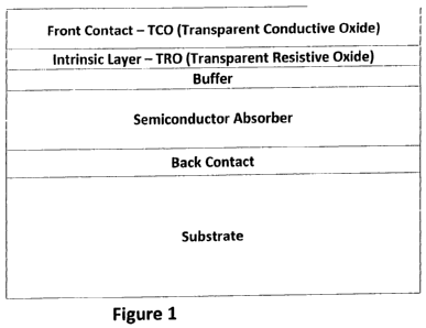
Figure 1 is a schematic view of a solar cell showing the relative positioning
of
the principal layers of the solar cell including a transparent conductive
oxide film
formed in accordance with the present invention;
Figures 2A-2C are graphic views showing an embodiment of a planar metal
target of indium-zinc used in a reactive sputtering process to form the
transparent
conductive oxide layer;
Figures 3A-3C are graphic views showing an embodiment of a rotatable metal
target of indium-zinc in the form of a rotatable cylinder used in a reactive
sputtering
process to form the transparent conductive layer; and
Figure 4 is a schematic view of a closed-loop feedback control system for
controlling the oxygen flow in the reactive sputtering process of the present
invention.
Detailed Description of the Invention
The present invention is generally directed to a method of forming a
transparent conductive oxide film (TCO) on a substrate which can be used as a
front
contact in the formation of articles such as solar cells and flat display
panels. As
shown in Figure 1, a typical solar cell known in the art is identified by
reference
number 1. The solar cell has a substrate 2 made of a supporting material such
as
glass covered by a back contact 3 composed of, for example, molybdenum. An
absorber layer 4 in the form of a thin film is spaced between the back contact
and a
front contact 5 comprised of the transparent conductive oxide. The prior art
TCO's
have been made from indium-tin oxides or aluminum-doped zinc oxides sputtered
4
CA 02740363 2011-04-12
WO 2010/090740 PCT/US2010/000310
from ceramic targets. The absorber layer 4 is typically a layer comprised of
copper-
indium selenide (CIS), copper-gallium selenide (CGS), copper-indium-gallium-
selenide (CIGS and CIGSS).
A buffer layer 6, typically made of gallium and/or indium oxide is positioned
above the absorber layer 4. Optionally a transparent resistive oxide (TRO)
layer 7 is
provided between the front contact 5 and the buffer 6. The TRO, also referred
to as
an intrinsic layer, is often made from zinc oxide obtained from sputtering of
a ceramic
target comprised of zinc oxides or reactive sputtering from a metal zinc
target. The
TRO is a low carrier density material which prevents the flow of electrons
between
the front contact 5 and the absorber layer 4.
In accordance with the present invention, there is provided a method of
forming the transparent conductive oxide by sputtering a metal target,
preferably
comprised of indium and zinc, in a controlled oxygen atmosphere as hereinafter
described, to produce a thin film comprised of indium and zinc oxide having
properties particularly suited for use as a front contact of a solar cell.
As compared with conventional TCO films made of aluminum-zinc oxide, the
TCO films of the present invention are thinner while exhibiting greater light
transmission and lower sheet resistance (ohm/square). In particular, to
achieve
similar sheet resistance, the TCO of the present invention is thinner,
typically only
5
CA 02740363 2011-04-12
WO 2010/090740 PCT/US2010/000310
about half as thick as needed for aluminum-zinc oxide films and exhibits light
transmission gains of 3-4%.
The method of the present invention is carried out by sputtering an indium-
zinc target with a gas mixture that consists of inert gas and reactive gas
(e.g.
oxygen). The principles of reactive sputtering are described in Reactive
Sputter
Deposition, Springer Series in Materials Science, Volume 109. Eds. Diederik
Depla
and Stijn Mahieu (2008). Inert gases such as argon are preferred gases for
sputtering the metal target. The shape of the metal target can affect the cost
of
producing the TCO. In one embodiment of the invention, the target is a planar
target
in the shape of a rectangular solid. A more preferred metal target is in the
form of a
rotatable cylinder.
As shown in Figure 2A, a planar target 10 made of indium-zinc (In-Zn) is
comprised of an In-Zn layer 11 situated on a backing plate 12. The layer 11 is
bombarded with an inert gas in an oxygen controlled environment to deposit
indium-
zinc oxide as the TCO thin film. The indium zinc layer 11 is comprised of
InxZn1_x
wherein x is from about 0.01 to 0.95, preferably from about 0.6 to 0.9.
During the sputtering process, a magnetic field 14 (shown in Figure 2B) is
established proximate the planar target. The intensity of the magnetic field
over the
length of the target (i.e. magnetic field distribution) is greatest at
locations (a) and
(b), respectively and decreases toward the center (c) and endpoints (d) and
(e).
6
CA 02740363 2011-04-12
WO 2010/090740 PCT/US2010/000310
Accordingly, the pattern of release of indium and zinc from the target is
greatest at
locations (a) and (b) where the intensity of the magnetic field is the
greatest. As can
be observed from Figure 2C, the useful life of the planar target is limited to
the extent
that the quantity of indium-zinc is exhausted at locations (a) and (b).
Conversely, the
metal remaining at locations (d), (c), and (e) is unused, which makes the
planar
target use somewhat inefficient.
As shown in Figures 2A-2C, the pattern of usage of the target metal for
reactive sputtering in the presence of oxygen is non-uniform and correlates to
the
magnetic field distribution. Target utilization may typically be in the range
of 25-30%.
A more uniform magnetic field distribution is shown in the embodiment of
Figures 3A-3C.
In accordance with a preferred embodiment of the invention, the metal target
is in the form of a rotatable cylinder which during the sputtering process
provides a
relatively uniform magnetic field distribution. Referring to Figure 3A, there
is shown
an indium-zinc target in the form of a rotatable cylinder (i.e. a rotary
target). The
rotary target 20 has a hollow core 22 and a shell 24 comprised of the target
metal
(e.g. indium-zinc) which is secured to a support or backing tube 26. The
target is
rotated during the sputtering process to generate a relatively uniform
magnetic field
28 as shown in Figure 3B. The magnetic field distribution is slightly higher
than
average at the respective ends (f) and (g) of the target, but is relatively
continuous
7
CA 02740363 2011-04-12
WO 2010/090740 PCT/US2010/000310
over much of the length (h) of the target. Because the magnetic field is
relatively
uniform over much of the length of the target, utilization of the target
material is more
uniform, often achieving 70-80% utilization.
Referring to Figure 3C, there is shown a representation of a pattern of target
erosion typically obtained for a rotary target. Much of the target metal has
been
released for forming the transparent conductive oxide. Only a relatively small
amount of the target material 30 remains on the backing tube 26. Utilization
of the
target material is terminated at locations (f) and (g) because the slightly
higher than
average magnetic field distribution at the respective ends (f) and (g) of the
rotary
target (see Figure 3B) fully erodes the target metal at these locations.
The indium-zinc metal target in either the planar or rotary form can be
sputtered under moderate pressure of about 3 to 10 mTorr, preferably about 7m
Torr
at a moderate power level of about 3 to 15 kW, preferably at about 10 kW. The
TCO
film produced in this manner provides a film with a sheet resistance of from
about 10
to 90 ohm/square, preferably about 20 ohm/square and a light transmission rate
of at
least 85% at a thickness of only about 200 to 250 nm, which is up to half the
thickness of a transparent conductive film made of aluminum doped zinc oxide
from
a ceramic target.
The benefits of using metal targets to produce the transparent conductive
oxide are realized in part by controlling the oxygen atmosphere during the
sputtering
8
CA 02740363 2011-04-12
WO 2010/090740 PCT/US2010/000310
process. If the oxygen content exceeds a desirable level, then the TCO film
will be
less conductive because of low carrier concentration due to lack of oxygen
vacancies. If the oxygen content falls below a desirable level, then the TCO
film will
exhibit light transmission and be more metal-like due to loss of mobility.
Accordingly, in a further embodiment of the invention, means are provided to
control the oxygen atmosphere during the sputtering process. In a preferred
embodiment, a feedback control system is used to monitor and control oxygen
levels
by associating the oxygen level with a monitorable variable of the system.
Such
monitorable variables include voltage, 02 partial pressure and plasma
emission.
Referring to Figure 4, there is shown a schematic view of a feedback control
system in which a select variable as mentioned above is associated with oxygen
levels. The variable is monitored and compared to a standard which correlates
with
adjustments that may be necessary to the oxygen levels. The feedback control
system of Figure 4 will be explained below in which voltage is employed as the
select variable.
The feedback control system 30 is comprised of a reference 32 which stores a
target voltage set point. The target voltage is a voltage level that
correlates with a
desirable oxygen level. The desirable oxygen level is that flow of oxygen into
the
system which produces a desirable transparent conductive oxide by the reaction
of
oxygen with metal from the metal target (e.g. InZn).
9
CA 02740363 2011-04-12
WO 2010/090740 PCT/US2010/000310
A sensor 34 continuously measures the actual voltage in the system and
generates a signal (measured output) corresponding to the measured voltage
which
is sent continuously or intermittently to the reference 32. When a deviation
between
the target voltage and the actual voltage is detected, a signal is sent to a
controller
36 which monitors the mass flow of oxygen to the system. The controller
adjusts the
flow of oxygen (system input) until the actual voltage and target voltage are
sufficiently similar so that the deviation between the target and actual
voltage is
either eliminated or sufficiently small that the flow of oxygen to the system
is
acceptable. For example, if the actual voltage exceeds the target voltage by
an
amount sufficient to cause a positive deviation (i.e. +deviation), oxygen flow
will be
increased. Conversely, if the actual voltage is less than the target voltage
by an
amount sufficient to cause a negative deviation (i.e. -deviation), oxygen flow
will be
decreased.
The feedback control system described in connection with Figure 4 can be
modified to employ 02 partial pressure as the monitorable variable. In this
embodiment, the reference is configured to establish an 02 partial pressure
set point.
The sensor detects the actual 02 pressure while the controller adjusts the
oxygen
flow to compensate for changes in the 02 partial pressure. The system output
monitors the actual 02 partial pressure as detected by the sensor. The system
input
corresponds to a signal corresponding to the flow of oxygen from the
controller to
provide a desirable flow of oxygen to the reactive sputtering process.
CA 02740363 2011-04-12
WO 2010/090740 PCT/US2010/000310
Another use of the feedback control system employs 02 plasma emission as
the monitorable variable. In this embodiment, the reference is configured to
establish an 02 plasma emission set point. The sensor detects the actual 02
plasma
emission while the controller adjusts the oxygen flow to compensate for
changes in
the 02 plasma emission. The system output monitors the actual 02 plasma
emission
as detected by the sensor. The system input corresponds to the flow of oxygen
from
the controller to provide a desirable amount of oxygen for the reactive
sputtering
process.
The present invention may also provide for a transparent resistive oxide
(TRO) layer to protect the photovoltaic device from an undesirable flow of
electrons.
As indicated in connection with Figure 1, solar panels employing a TCO in
accordance with the present invention may also include a transparent resistive
oxide
layer between the TCO and the buffer. It is preferred in the present invention
to
employ a TRO comprised of indium-gallium-zinc oxide (IGZO) and/or indium-
aluminum-zinc oxide (IAZO).
The TRO can be produced using metal targets having a desired metal
composition (e.g. indium, gallium and zinc) in a manner similar to the method
for
producing the TCO. For example, a metal target comprised of indium, gallium
and
zinc is sputtered in a controlled oxygen atmosphere. The target may be planar
or
11
CA 02740363 2011-04-12
WO 2010/090740 PCT/US2010/000310
preferable a rotary target and the system may control the oxygen levels by
employing a feedback control system as described in connection with Figure 4.
Example 1:
An InZn target was sputtered by argon for twenty-four hours in a continuous
operation at a constant power mode at a pressure of about 7mTorr to produce a
TCO on a glass substrate. The resulting indium-zinc oxide (IZO) film had a
thickness of from 243-244 nm, a sheet resistance of from 21.4-21.6 ohm/square
and
a light transmission rate of from 87%-88%. The process was conducted with the
benefit of a closed-loop feedback control of the cathode voltage as described
in
connection with Figure 4.
As a comparison, a conventional TCO film utilizing a metal target made of
AZO (AI:ZnO) with similar electrical properties as the IZO film had a
thickness of
500-550 nm thickness, a sheet resistance of 23-24 ohm/square and a light
transmission rate of 84-85%. Therefore, to achieve similar sheet resistance,
only
about half of the required AZO film thickness is needed with IZO films
prepared in
accordance with the present invention with an absolute light transmission gain
of 3-
4%.
Example 2:
The deposition rate from an InZn target was computed based on typical
production runs of solar panels. At a power level of 10 kW, films having a
thickness
12
CA 02740363 2011-04-12
WO 2010/090740 PCT/US2010/000310
of about 243 nm were produced at a line speed of 40 cm/min. The dynamic
deposition rate (DDR) was calculated to be 960 nm.cm/min/kW. Converted to
effective deposition rate in nm/min, the deposition rate in this example is
756 nm/min
at 10 kW. This deposition rate can be increased relatively easily to over 1
pm/min
provided a higher power is used during the sputtering process.
20
13