Note: Descriptions are shown in the official language in which they were submitted.
CA 02747294 2011-06-16
WO 2010/041067 PCT/GB2009/051334
1
Improvements relating to Power Adaptors
This invention relates to power adaptors, and in particular power adaptors
suitable
for providing a change in effective voltage between the input and the output
of the
power adaptor.
In domestic applications, the voltage available from the mains supply is
typically
120V-240V AC, at frequencies of 50 or 60 Hz. Where a power adaptor is adapted
to drive a low voltage load, such as a 10V load, the ratio between the voltage
available at the supply and the voltage required to drive the load is between
10
and 20. With such a large ratio, conventional switched-mode power adaptors
used to drive low voltage loads become very inefficient because the switching
operates at small duty ratios with very short conduction times and current
waveforms having high peak to average ratios.
It is common therefore in prior art power adaptors to include a magnetic
transformer with a turns ratio suitable to create a step down in voltage and a
corresponding step up in current. In some conventional power supplies, this
magnetic transformer is provided at the input to the power adaptor, such that
the
entire power adaptor operates at lower voltage. In such cases, the magnetic
transformer operates at a supply frequency (50 or 60 Hz) and is relatively
bulky
and expensive. In other cases, the magnetic transformer is integrated as part
of
the switching circuit, allowing it to operate at the switching frequency of
the
electronic components in the power adaptor. Such circuits therefore have the
advantage that the magnetic transformer can be made smaller.
Nevertheless, all of these prior art arrangements require a magnetic
transformer,
which is rather bulky and inefficient.
There has now been devised an improved power adaptor which overcomes or
substantially mitigates the above-mentioned and/or other disadvantages
associated with the prior art.
CA 02747294 2011-06-16
WO 2010/041067 PCT/GB2009/051334
2
According to the invention, there is provided a power adaptor comprising an
input
for connection to an AC power supply, and a resonant circuit coupled to the
input
that provides an output suitable for driving a load, wherein the capacitance
and
inductance of the resonant circuit are selected to provide a pre-determined
change
in effective voltage, and a corresponding pre-determined change in effective
current, between the input and the output of the power adaptor.
The power supply according to the invention is advantageous principally
because
the power adaptor provides a pre-determined change in effective voltage, and a
corresponding pre-determined change in effective current, between the input
and
the output of the power adaptor, without any need for a magnetic transformer.
The
power adaptor may therefore be adapted to drive a low voltage load from a
higher
mains AC supply, without the need for a magnetic transformer, and without the
need for an electronic switching circuit operating at small duty ratios (short
on-
times relative to switching periods) and having current waveforms with high
peak
to average ratios. In particular, the power adaptor may be adapted to connect
to a
high voltage AC mains supply (eg 110V or 230V AC, at frequencies of 50Hz or
60Hz), and provide an output suitable for driving a low voltage solid state
light
source (eg 10-20V).
The capacitance and inductance of the resonant circuit may be selected to
provide
a pre-determined decrease in effective voltage, and a corresponding pre-
determined increase in effective current, between the input and the output of
the
power adaptor. Alternatively, the capacitance and inductance of the resonant
circuit are selected to provide a pre-determined increase in effective
voltage, and a
corresponding pre-determined decrease in effective current, between the input
and the output of the power adaptor.
In presently preferred embodiments, the capacitance and inductance of the
resonant circuit are selected to provide a pre-determined ratio between the
effective voltage at the input of the power adaptor and the effective voltage
at the
output of the power adaptor, and a pre-determined ratio between the effective
current at the input of the power adaptor and the effective current at the
output of
the power adaptor.
CA 02747294 2011-06-16
WO 2010/041067 PCT/GB2009/051334
3
The resonant circuit is preferably configured to provide an output having an
increased or decreased effective current relative to the effective current
through a
resonant inductor, such that the output has a correspondingly decreased or
increased effective voltage relative to the effective voltage of the power
supply.
The output preferably has an effective current that is increased or decreased
relative to the current through the resonant inductor by a factor of at least
two, and
most preferably by a factor of at least five. In addition, the effective
voltage
decrease or increase of the output relative to the AC power supply is
preferably by
a factor of at least two, and most preferably by a factor of at least five.
The pre-determined changes in effective voltage and effective current between
the
input and the output of the power adaptor are preferably achieved with no
assistance from a magnetic transformer. Indeed, the power adaptor may be
devoid of any magnetic transformers, other than signal or power supply
transformers, which may be present in the power adaptor.
The pre-determined changes in effective voltage and effective current between
the
input and the output of the power adaptor may be achieved with no assistance
from a transformer. However, the power adaptor may be provided with a
piezoelectric transformer that isolates the output from the input of the power
adaptor. In this arrangement, the piezoelectric transformer may provide a
further
pre-determined change in effective voltage, and a further pre-determined
change
in effective current, between the input and the output of the power adaptor.
Where the power adaptor is provided with a piezoelectric transformer, the
piezoelectric transformer may be arranged to provide at least some of the
capacitance of the resonant circuit. In one embodiment, the piezoelectric
transformer provides all of the capacitance of the resonant circuit. The
inclusion of
a piezoelectric transformer therefore offers several advantages when
incorporated
into a power adaptor having a resonant circuit. Hence, according to a further
aspect of the invention, there is provided a power adaptor comprising an input
for
connection to an AC power supply, a resonant circuit coupled to the input that
CA 02747294 2011-06-16
WO 2010/041067 PCT/GB2009/051334
4
provides an output suitable for driving a load, and a piezoelectric
transformer that
isolates the output from the input of the power adaptor.
The output is preferably suitable for driving a constant current load, such as
a solid
state light source. The resonant circuit is preferably therefore configured to
provide an output having a substantially constant voltage, which is pre-
determined
for a particular effective voltage of the AC power supply. In particular, the
resonant circuit is preferably configured to either boost (ie raise) or buck
(ie lower)
the actual voltage received at the input of the power adaptor, in order to
provide a
substantially constant voltage, which is pre-determined for a particular
effective
voltage of the AC power supply, for the majority of the input AC cycle.
This arrangement of the present invention therefore enables the output to have
a
substantially constant voltage, which is pre-determined for a particular
effective
voltage of the AC power supply, for a greater proportion of the input AC cycle
than
that provided by a magnetic transformer. This arrangement therefore enables
the
power adaptor to have a lower bulk storage capacitance than power adaptors
that
utilise magnetic transformers to provide a pre-determined change in effective
voltage.
This arrangement of the present invention is suitable for driving fixed loads.
However, the power adaptor may also be adapted to drive variable loads. In
particular, the power adaptor may be adapted to turn off the output, when the
load
is insufficient to be driven by the output provided by the power adaptor, and
then
turn on the output when the load is sufficient to be driven by the output
provided by
the power adaptor.
In a particularly preferred arrangement for providing an output that is
suitable for
driving a constant current load, the resonant circuit is an LCL series-
parallel
resonant circuit.
By "LCL series-parallel resonant circuit" is meant a resonant circuit
comprising a
first inductor and a first capacitor in series, and a parallel load leg
including a
second inductor. The first inductor and first capacitor are preferably
connected in
CA 02747294 2011-06-16
WO 2010/041067 PCT/GB2009/051334
series between two input terminals of the resonant circuit, and the resonant
circuit
preferably comprises a load leg connected in parallel across the first
capacitor,
wherein the load leg comprises the second inductor and an output for driving
the
load, which are connected in series. In particular, the LCL resonant circuit
5 preferably has input terminals and output terminals with a first inductor
L1,
connected from a first input terminal through a common point with second
inductor
L2, to a first output terminal, the second input terminal being directly
connected to
the second output terminal, and a capacitor C1, connected between the common
point between the two inductors and the direct connections between second
terminals of input and output. The input terminals are preferably adapted to
be
driven from a high frequency inverter. Any of the first inductor, the first
capacitor
and the second inductor may comprise a single inductive or capacitive
component
or a combination of such components.
The resonant circuit is preferably adapted such that at one of its resonant
frequencies, the power adaptor provides a constant current output, at a given
effective input voltage, and the resonant circuit is preferably driven at that
resonant
frequency or a sub-harmonic thereof, or sufficiently near to that resonant
frequency or a sub-harmonic thereof for the power adaptor to be suitable for
use
with a constant current load, such as a solid state light source. In
particular, the
first and second inductors are preferably selected such that the reactance XL1
of
the first inductor and the reactance XL2 of the second inductor are
substantially
equal in magnitude, and are substantially equal in magnitude to the reactance
Xci
of the first capacitor. In particular, XL1 x XL2 -Xci in presently preferred
embodiments.
When the chosen components satisfy these conditions, at a given input voltage,
the current delivered to a load will be constant, independent of the load
connected
to the power adapter. Furthermore, variation of the input voltage would
directly
control the magnitude of the constant current delivered to the load. When
driving
a constant voltage load, such as LEDs, the power delivered to the load would
therefore be directly proportional to the input voltage, without requiring any
feedforward or feedback control.
CA 02747294 2011-06-16
WO 2010/041067 PCT/GB2009/051334
6
Where the LCL series-parallel resonant circuit is adapted to provide a
constant
current output, the capacitance of the LCL series-parallel resonant circuit is
preferably selected with a reactance Xc1 to match a required load resistance
RL
and a required, relatively higher, input resistance R;nfor the resonant
circuit. The
first capacitor is preferably selected using the following equation:
X CI = Rin RL (1
where Xc, is the reactance of the first capacitor. The reactance of the first
capacitor is preferably therefore equal to the square-root of the product of
the
required load resistance RL and the required input resistance R;n for the
resonant
circuit.
The output of the power adaptor is preferably therefore adapted to be
connected
to a load of apparent impedance RL, the value of the first and second
inductors,
and the first capacitor, L1, L2 and C1, being chosen such that at least one
frequency, the reactances of L1, L2 and C1 are approximately similar in
magnitude
and that at least one frequency the apparent impedance seen at the input
terminals R;n is transformed by the LCL resonant circuit to be approximately
equal
to the square of the reactance of the capacitor Xcl divided by the apparent
impedance of the load, RL.
This selection of the inductance and capacitance of the resonant circuit
therefore
provides a pre-determined change in effective voltage between the input and
the
output of the power adaptor.
In presently preferred embodiments, the power adaptor according to the
invention
comprises an input for connection to a mains AC power supply, and the resonant
circuit provides an output suitable for driving a solid state light source. As
discussed above, the resonant circuit is preferably an LCL series-parallel
resonant
circuit.
CA 02747294 2011-06-16
WO 2010/041067 PCT/GB2009/051334
7
The use of an LCL series-parallel resonant circuit is particularly
advantageous
when the power adaptor is adapted to provide an output suitable for driving a
solid
state light source. In particular, the LCL series-parallel resonant circuit
may be
adapted to provide a constant current output suitable for driving a solid
state light
source, which is not dependent upon the load, and does not require any form of
feedback or complex control. A power adaptor including an LCL series-parallel
resonant circuit may therefore provide a much more efficient transfer of power
from the mains power supply to the solid state light source, in comparison to
prior
art power adaptors, and the power adaptor may be more compact and have a
lower manufacturing cost than prior art adaptors. In addition, the power at
the
output of the power adaptor would typically reduce as the input power reduces,
and hence a power adaptor including an LCL series-parallel resonant circuit is
suitable for use with conventional power reducing devices associated with the
mains power supply. Hence, according to a further aspect of the invention,
there
is provided a power adaptor for a solid state light source, the power adaptor
comprising an input for connection to a mains power supply, and an LCL series-
parallel resonant circuit coupled to the input that provides an output
suitable for
driving the solid state light source.
The resonant circuit is preferably adapted to provide, at a given input
voltage, a
constant current output. The power delivered to the output preferably
therefore
varies with variation of the voltage at the input, with no need for any
control. In
particular, the magnitude of the constant current is preferably proportional
to the
input voltage. Furthermore, the resonant circuit is preferably adapted to
provide,
at a given input voltage, a constant current output that is independent of the
load.
In order to achieve these characteristics, the resonant circuit is preferably
adapted
such that one of its resonant frequencies provides these properties, and the
resonant circuit is preferably driven at that resonant frequency, or
sufficiently near
to that resonant frequency for the power adaptor to be suitable for use with a
solid
state light source.
Nevertheless, it has been found that by driving the resonant circuit at a sub-
harmonic of the resonant frequency, the power factor and/or efficiency of the
CA 02747294 2011-06-16
WO 2010/041067 PCT/GB2009/051334
8
power adaptor may be improved. Most preferably, the resonant circuit is driven
at
a sub-harmonic of 1/x, where x is an odd number, for example, 1/3, 1/5 or 1/7.
Driving the resonant circuit at a sub-harmonic of the resonant frequency has
the
advantage that the switching frequency and switching losses of the resonance
drive circuit may be reduced, thereby improving the efficiency of the power
adaptor. In most prior art resonant circuits, driving the circuit at a sub-
harmonic
would reduce the power. However, the LCL series-parallel resonant circuit may
be
adapted to have one of its resonant frequencies at 0 Hz, as discussed in more
detail below, which allows low frequency currents to pass through to the load.
Hence, the current passing through the resonant circuit and the power
delivered to
the load does not change substantially if the circuit is driven at a sub-
harmonic of
the resonant frequency.
The LCL series-parallel circuit maybe adapted to have three resonant
frequencies,
a first resonant frequency at OHz, ie DC current, a second resonant frequency
that
provides, at a given input voltage, a constant current output that is
independent of
the load, and a third resonant frequency that provides, at a given input
voltage, a
current that varies with load. These resonant frequencies are preferably
achieved
by selecting the first inductor, the second inductor and the first capacitor,
such that
the reactances of those components are substantially equal. The third resonant
frequency may be adapted to provide a significantly greater power at the
output,
relative to the second resonant frequency. A controller of the power adaptor
may
therefore be adapted to switch between the different resonant frequencies in
order
to utilise their different characteristics. For example, a controller of the
power
adaptor may be adapted to switch between the second and third resonant
frequencies to compensate for a change of input voltage, eg between 230V and
110V AC. Further examples of such control include loading a TRIAC in the
lighting system at critical points, and altering the power factor and/or
regulation of
the power adaptor.
As the voltage at the input varies sinusoidally, the current drawn from the
input by
an LCL series-parallel resonant circuit, configured as described above, will
inherently follow a square shape. However, the waveform of the current drawn
CA 02747294 2011-06-16
WO 2010/041067 PCT/GB2009/051334
9
from the input by the resonant circuit may be modified by a controller of the
power
adaptor. The power adaptor may therefore include a controller adapted to
determine the waveform of the current drawn from the input by the resonant
circuit. In particular, the controller may be adapted to modify the waveform
of the
current that would inherently be drawn by the resonant circuit, such that the
waveform of the current drawn from the input is more similar in shape to the
waveform of the voltage at the input. In particular, the current drawn by the
resonant circuit may have a waveform that is generally sinusoidal, but with
flattened peaks.
The resonant circuit is preferably driven by a resonance drive circuit, which
provides a resonance drive signal to the resonant circuit. The resonance drive
signal is preferably an alternating signal, and is preferably provided by an
oscillator
that may control two or four electronic switches, eg FETs. The resonance drive
signal typically has the form of a square wave. The purpose of the drive
circuit is
to excite the resonant circuit with an alternating voltage, the alternating
voltage
typically consisting of blocks of positive and negative voltage. The
electronic
switches are typically connected together in the form of a full bridge
inverter
(4 switches) or a half bridge inverter (2 switches).
As discussed above, the power adaptor may be adapted to modify the waveform
of the current that would inherently be drawn by the resonant circuit, and in
particular modify the shape and/or size of that waveform. In particular, a
resonance drive signal may be provided to the resonant circuit, wherein the
resonance drive signal is adapted to determine the desired input current
waveform. For instance, the resonance drive signal may be adapted in a variety
of
ways including, but not limited to, any of the following including
combinations
thereof: (i) introducing a dead-band between half-cycles or full cycles of the
alternating drive signal, (ii) varying the frequency of the drive signal, and
(iii)
missing cycles of the alternating drive signal.
Where the resonance drive signal is adapted by missing cycles of the
alternating
drive signal, these missing cycles may be arranged in a discontinuous
arrangement, in a single continuous group, or in a plurality of continuous
groups,
CA 02747294 2011-06-16
WO 2010/041067 PCT/GB2009/051334
for each mains supply cycle. Where the missing cycles are arranged in a
plurality
of continuous groups, the number of continuous groups for each mains supply
cycle is preferably selected to be appropriate for the output power, and hence
may
be variable with the output power.
5
As discussed below, the power adaptor may be adapted to control the light
output
from the solid state light source. In this embodiment, the resonance drive
signal is
preferably variable, for example by a controller, in order to determine the
light
output from the solid state light source. The resonance drive signal is
preferably
10 also adapted to optimise the power factor and/or efficiency of the power
adaptor.
Alternatively, where the power adaptor is configured such that the light
output from
the solid state light source is only controllable by varying the power
available at the
input of the power adaptor, the resonance drive signal may be predetermined,
preferably to optimise the power factor and/or efficiency of the power
adaptor.
Any controller of the power adaptor, as discussed above, is preferably adapted
to
control the resonant drive signal provided to the resonant circuit, in order
to
determine the waveform of the current drawn from the input by the resonant
circuit. This controller of the power adaptor may be provided by an integrated
circuit, such as a microprocessor, an analogue electronic circuit, or any
combination of analogue and digital electronics. Indeed, the controller of the
power adaptor may be an application specific, integrated circuit, which may be
manufactured at very low cost. In this configuration, the oscillator of the
drive
circuit may also form part of the integrated circuit, or may be a separate
circuit.
The determination of the frequency at which the resonant circuit is driven may
be
used to calibrate the power adaptor for improved efficiency. Alternatively,
the
frequency at which the resonant circuit is driven may be varied during use, in
order
to vary the power being supplied to the solid state light source.
The output for driving the solid state light source may be isolated from the
resonant circuit, particularly for applications in which users would have
access to
CA 02747294 2011-06-16
WO 2010/041067 PCT/GB2009/051334
11
the solid state light source and/or associated circuitry. In this case, the
power
adaptor preferably comprises a piezoelectric transformer to provide this
isolation.
The resonant circuit may also include a pair of potential dividing capacitors,
to
which the first capacitor is connected. Alternatively, where the resonance
drive
circuit contains four electronic switches (eg FETs) arranged to create two
switching legs (eg a "H-bridge"), as a single phase inverter, the pair of
capacitors
could be replaced by a single capacitor. These capacitors are preferably Y
capacitors.
In another embodiment, the resonance drive circuit comprises two electronic
switches (eg FETs) connected between the LCL series-parallel resonant circuit
and ground, ie two "low-side" switches. These two low-side switches preferably
each alternate between ON and OFF, which a first switch being ON whilst a
second switch is OFF, and vice versa. This arrangement is particularly
advantageous where the switches are driven by a low voltage controller, such
as
an integrated circuit.
In this embodiment, the first resonant inductor of the LCL series-parallel
resonant
circuit preferably comprises two inductors, one connected to one end of the
first
capacitor, and the other connected to the other end of the first capacitor. In
this
arrangement, one of these two inductors will be active in the positive half
cycle of
the supply, and the other of these two inductors will be active in the
negative half
cycle of the supply. In one embodiment, these two inductors are wound about a
common core, such that the first resonant inductor of the LCL series-parallel
resonant circuit is a three terminal inductor.
The power adaptor may draw current from the input as a function of the voltage
at
the input in order that the power adaptor appears as a resistive load to the
mains
supply. This is preferably achieved by: (i) minimising the capacitance at the
input
of the power adaptor, (ii) drawing a current waveform from the input that is
substantially in phase with the voltage waveform at the input, and/or (iii)
drawing
current that is substantially proportional to the voltage. These features
reduce
current distortion and harmonic currents drawn from the mains supply, and
CA 02747294 2011-06-16
WO 2010/041067 PCT/GB2009/051334
12
increase the efficiency and power factor of the power adaptor by removing the
capacitive load presented to the mains supply. Indeed, these features enable
the
power adaptor and connected solid state light source to be presented to the
mains
supply as a conventional filament light source.
Alternatively, the power adaptor may draw power from the input as a function
of
the voltage at the input, such that the power adaptor does not appear as a
resistive load to the mains supply.
The solid state light source is preferably a Light Emitting Diode (LED), or a
series
of two or more LEDs. The power adaptor preferably includes one or more diodes
at its output, eg a diode bridge, to ensure that no reverse currents are
present that
could damage the solid state light source.
Any control circuitry of the power adaptor may be powered by an integrated
power
supply. Alternatively, the control circuitry of the power adaptor may be
powered by
a connection to one of the inductors of the resonant circuit, for instance a
connection to a winding coupled to that inductor.
Where the power adaptor includes an integrated power supply, the integrated
power supply preferably draws power directly from the mains power supply, most
preferably via the input of the power adaptor. In particular, the integrated
power
supply is preferably a constant current power supply, such as a switch mode
constant current regulator, which preferably does not cause excessive inrush
and
is low in cost. The control circuitry is preferably adapted to shut itself
down during
the off periods of a mains cycle, for example when the power adaptor is
connected
to a TRIAC or similar device, so that the constant current device can be low
in
power and hence the efficiency high.
The power adaptor preferably also includes a fault detection circuit that
disables
the resonant circuit, preferably by removing the oscillating drive signal, in
the event
that the load is removed, which may be caused by failure or disconnection of
the
light source, for example. The fault detection circuit preferably connects an
output
of the resonant circuit with the controller. This fault detection circuit is a
feedback
CA 02747294 2011-06-16
WO 2010/041067 PCT/GB2009/051334
13
circuit, but it preferably draws minimal power from the output of the resonant
circuit
during normal operation, and hence should not be confused with an active
feedback circuit that regulates the power output. The fault detection circuit
would
be active during a fault condition only, and is not essential for controlling
the output
power during normal use.
The power adaptor may include a filter at its input for reducing harmonic
currents
drawn from the mains supply. The filter may comprise a small non-electrolytic
capacitor-inductor network. The power adaptor preferably also includes a
rectifier
at its input that converts the input waveform to one of constant polarity.
Most
preferably, the rectifier is a full wave rectifier that reverses the negative
(or
positive) portions of the alternating current waveform. Nevertheless, there is
no
need for the power adaptor to provide a steady DC signal at the input of the
LCL
series-parallel resonant circuit, and hence a bulk storage capacitor (also
known as
a reservoir capacitor or smoothing capacitor) is preferably not provided
between
the input of the power adaptor and the LCL series-parallel resonant circuit.
Hence,
the power adaptor is preferably substantially free of bulk storage capacitance
between the input of the power adaptor and the resonant circuit. Indeed, the
power adaptor is preferably substantially free of electrolytic capacitors.
This
enables the supply to be designed with minimal reactance, minimal inrush
current,
and long life with reduced size and cost relative to prior art power adaptors
for
solid state lighting systems. A bulk storage capacitor may be provided at the
output of the power adaptor, but this is not essential for the functioning of
the
power adaptor with a conventional solid state light source.
The power adaptor according to the invention is preferably suitable for use in
a
lighting system that utilises any power reducing device for determining the
power
available at the input of the power adaptor. In particular, the power reducing
device may be a variable resistor, such as a Variac, or a rheostat. The power
adaptor may also be adapted to function in lighting systems that include a
dimmer
control utilising SCR phase control or a triac in order to reduce the power
available
at the input of the power adaptor. In this case, however, the power adaptor
may
be adapted to draw a minimum current from the mains supply to keep the SCR
CA 02747294 2011-06-16
WO 2010/041067 PCT/GB2009/051334
14
stable during the full mains cycle, unless the lighting unit is switched off,
to ensure
the continued functioning of the dimmer control.
A further advantage of the power adaptor according to the invention is that no
monitoring of the voltage at the input, for example by a controller of the
power
adaptor, is necessary. Hence, the power adaptor according the invention may be
devoid of any means for monitoring the voltage at the input, and in particular
the
power adaptor may be adapted such that the controller does not receive a
signal
from the input.
The power adapter may include a controller able to deliver a control signal to
the
resonant circuit for reducing power drawn from the input. However, in other
embodiments, the power adaptor does not include a controller having such a
feature. In particular, the power adaptor may be adapted so that the light
output
from the solid state light source is only controllable by varying the power
available
at the input of the power adaptor. In particular, the power available at the
input of
the power adaptor may be varied using an external device, such as an external
power reducing device, associated with the mains supply. This embodiment is
particularly suitable for use with a lighting unit including an integral power
adaptor,
which would be suitable for incorporation into a conventional lighting
circuit. In
order to maximise the efficiency of the power adaptor, the power adaptor is
preferably adapted to transfer all power available at the input, save for
unavoidable losses, to the output of the power adaptor.
According to a further aspect of the invention, there is provided a lighting
system
comprising a power adaptor as described above and a lighting unit including at
least one solid state light source.
The lighting unit will typically be provided with a plurality of solid state
light
sources. In order to achieve different colours of light output, the lighting
unit may
include solid state light sources that emit light of different colours, for
example
LEDs that emit light of red, green and blue colour. Furthermore, the lighting
unit
may also include LEDs of amber, cyan and white colour in order to raise the
colour
rendering index.
CA 02747294 2011-06-16
WO 2010/041067 PCT/GB2009/051334
The power adaptor and the lighting unit may have a common housing, or may be
housed separately. Indeed, the power adaptor may be adapted to provide power
to a plurality of lighting units, each lighting unit including a plurality of
solid state
5 light sources. Furthermore, the lighting system may include a plurality of
such
power adaptors. The lighting system may also include a power reducing device,
such as a variable resistor, a rheostat or a dimmer control that utilises SCR
phase
control.
10 The power adaptor according to the invention is particularly suitable for
use with a
lighting unit including an integral power adaptor, which would be suitable for
incorporation into a conventional lighting circuit. Hence, according to a
further
aspect of the invention, there is provided a lighting unit suitable for direct
connection to a mains supply, the lighting unit comprising a power adaptor as
15 described above and one or more solid state light sources, in which the
light
output from the one or more solid state light sources is controllable by
varying the
power available at the input of the power adaptor. In order to maximise the
efficiency of the power adaptor, the power adaptor is preferably adapted to
transfer all power available at the input, save for unavoidable losses, to the
output
of the power adaptor.
The lighting unit preferably comprises a housing for accommodating the power
adaptor and the one or more solid state light sources, and a connector for
connecting the input of the power adaptor to the mains supply. The connector
is
preferably adapted to connect to a fitting for a conventional filament light
bulb. In
particular, the lighting unit may include a bayonet or threaded connector. In
one
embodiment, the light output from the one or more solid state light sources is
only
controllable by varying the power available at the input of the power adaptor.
According to a further aspect of the invention, there is provided an
electronic
impedance matching circuit incorporating an LCL resonant circuit with input
terminals and output terminals with a first inductor L1,connected from a first
input
terminal through a common point with second inductor L2, to a first output
terminal, the second input terminal being directly connected to the second
output
CA 02747294 2011-06-16
WO 2010/041067 PCT/GB2009/051334
16
terminal, and a capacitor C1, connected between the common point between the
two inductors and the direct connections between second terminals of input and
output , the input terminals being driven from a high frequency inverter, the
output
terminals being connected to a load of apparent impedance RL, the value of the
components L1, L2 and C1 being chosen such that at least one frequency, the
reactances of L1, L2 and C1 are approximately similar in magnitude and that at
least one frequency the apparent impedance seen at the input terminals is
transformed by the LCL resonant circuit to be approximately equal to the
square of
the reactance of the capacitor divided by the apparent impedance of the load,
RL.
The frequency of operation of the high frequency inverter is preferably close
to the
frequency where the reactances of L1, L2 and C1 are approximately similar.
The electronic impedance matching circuit is preferably adapted to drive one
or
more LEDs with a voltage requirement which is substantially lower than the
input
supply voltage.
Alternatively, however, the electronic impedance matching circuit may be
adapted
to charge a battery with a voltage requirement which is substantially lower
than the
input supply voltage, or may be adapted to drive an electric motor at more
than
one speed by dynamically matching the varying apparent load impedance to the
supply voltage.
A preferred embodiment of the invention will now be described in greater
detail,
by way of illustration only, with reference to the accompanying drawings, in
which
Figure 1 is a schematic diagram of a power adaptor according to the invention;
Figure 2 is a schematic diagram of a resonant circuit, including a resonance
controller and a resonance drive circuit, that forms part of the power adaptor
of
Figure 1;
Figure 3 is a schematic diagram of the resonant circuit of Figure 2, including
an
alternative resonant drive circuit;
CA 02747294 2011-06-16
WO 2010/041067 PCT/GB2009/051334
17
Figure 4 is a schematic diagram of a second alternative to the circuit shown
in
Figure 2;
Figure 5 is a schematic diagram of a third alternative to the circuit shown in
Figure 2;
Figure 6 is a schematic diagram of a fourth alternative to the circuit shown
in
Figure 2;
Figure 7 is a schematic diagram of a fifth alternative to the circuit shown in
Figure
2; and
Figure 8 is a schematic diagram of a lighting system according to the
invention.
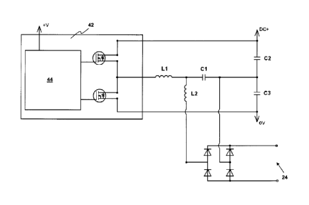
Figure 1 shows a power adaptor 20 according to the invention. The power
adaptor
comprises an input 22 for drawing electrical power from the mains circuit, and
an output 24 for providing electrical power to the three LEDs 60a,60b,60c of
the
solid state lighting unit 50. The power adaptor 20 includes a filtering and
rectifying
20 circuit 30 at the input 22, such that the AC voltage waveform drawn from
the mains
circuit is supplied to the remainder of the power adaptor circuitry as a full-
wave
rectified waveform (DC+).
The power adaptor 20 also includes a low power, auxiliary power supply 32, and
a
resonant circuit 34 including a resonance controller 40 and a resonance drive
circuit 42, which are described in more detail below with reference to Figure
2.
The low power, auxiliary power supply 32 provides a low power DC output (+V)
for
powering the integrated circuits of the resonance controller 40 and the
resonance
drive circuit 42. This provides a stable power supply to the integrated
circuits of
the power adaptor to ensure stable functioning of those circuits. It is noted
that in
other embodiments, the integrated circuits of the power adaptor are powered by
connections to additional windings coupled to one of the inductors of the
resonant
circuit, and hence the auxiliary power supply 32 is omitted.
CA 02747294 2011-06-16
WO 2010/041067 PCT/GB2009/051334
18
The resonant circuit 34, including the resonance controller 40 and the
resonance
drive circuit 42, is shown in Figure 2. The resonance controller 40 includes a
control circuit and is adapted to control the resonance drive circuit 42. In
particular, the resonance controller 40 has an output for supplying a control
signal
to the resonance drive circuit 42, which determines the form of the current
drawn
from the input by the resonant circuit 34. It is noted that in other
embodiments, the
resonance drive circuit 42 is self-oscillating, and the control circuit is
omitted
altogether.
The resonant circuit 34 has the form of an LCL series-parallel resonant
circuit (L1,
C1 and L2). The resonance drive circuit 42 is adapted to drive the LCL series-
parallel resonant circuit with a square wave driving signal. This square wave
signal is generated by two electronic switches, eg FETs, connected to a first
end
of the resonant circuit, and associated drive circuitry 44. The FETs are
controlled
by the resonance controller 40. The output of the resonant circuit 34 is
rectified
using a diode bridge, and then smoothed by a capacitor (C5) at the output of
the
rectifier, so as to form an output suitable for driving the LEDs 60a,60b,60c.
The
capacitors C2 and C3 create a connection point for the second end of the
resonant
circuit, substantially midway in voltage between DC+ and OV.
Alternatively, the resonance drive circuit 42 contains four electronic
switches (eg
FETs) arranged to create two switching legs (in a "H-bridge"), as a single
phase
inverter, as illustrated in Figure 3. In this embodiment, the capacitors C2
and C3
have been be replaced by a single capacitor (C2) connected between DC+ and
OV. The circuit cannot operate with no capacitance across the DC supply, as a
small amount of capacitance is required to protect the switches from
overvoltage
damage during switching transients.
The LCL series-parallel resonant circuit is configured such that at a chosen
frequency, the reactance of L1 (XL,), the reactance of C1 (Xc,) and the
reactance
of L2 (XL2) are substantially equal. In this configuration, the LCL series-
parallel
resonant circuit has two non-zero resonant frequencies. The frequency at which
the reactances are equivalent will be one of the two non-zero resonant
frequencies. When driving the resonant circuit at this frequency, the resonant
CA 02747294 2011-06-16
WO 2010/041067 PCT/GB2009/051334
19
circuit supplies a constant current to the output, and hence to the LEDs
60a,60b,60c, regardless of the load. The magnitude of the constant current is
proportional to the input voltage. This resonant frequency is
01 =+ 1 (2)
LSCP
The resonance controller 40 and the resonance drive circuit 42 is therefore
adapted to excite the LCL series-parallel resonant circuit close to this
resonant
frequency, wi. As a consequence of driving the resonant circuit close to the
resonant frequency, the switching losses in the electronic switches are
reduced,
and hence the efficiency of the circuit is improved. Further advantages
include the
reduction of conducted and radiated electromagnetic interference, and hence
the
reduction of the expense of necessary filtering and screening components.
The normal characteristic of this configuration of the LCL series-parallel
resonant
circuit is to draw a power which is directly related to input voltage. Without
any
control, as the voltage at the input 22 varies sinusoidally, the AC current
drawn
from the input 22 would follow a square shape. However, it is possible to use
the
on-time modulation and/or the frequency of the switches to reduce the power
drawn from the input 22 in the proximity of each zero crossing, and therefore
to
improve the input current harmonics. In addition, the optional capacitor (C5)
on
the output of the rectifier smoothes the power delivered to the LED such that
the
light output will contain less fluctuation.
A fault detection circuit is preferably provided that includes a connection
between
the output of the LCL series-parallel resonant circuit and a disable pin on
the PIC
of the resonance controller 40, through resistor R1, and a connection with OV
through resistor R2. The fault detection circuit draws minimal power. However,
in
the event that an LED 60a,60b,60c stops conducting, the associated fault
detection circuit quickly detects a rise in voltage at the output of the
resonant
circuit and causes the resonance controller 40 to shut-off its output to the
resonant
drive circuit 42, and hence cause the drive signal to be removed from the
resonant
circuit 34. In Figure 2, the fault detection circuit is shown connected
between L2
CA 02747294 2011-06-16
WO 2010/041067 PCT/GB2009/051334
and the diode bridge. However, please note that this circuit could also be
connected between the positive end of the diode bridge and the positive
terminal
of the output 24.
5 The amount of power delivered to the LEDs 60a,60b,60c can be varied with the
variation of the input mains supply voltage, which makes it suitable for use
with a
power reducing device 10.
Figure 4 shows a further alternative to the circuit shown in Figure 2, in
which the
10 resonance controller 40 has been omitted. In this embodiment, the resonance
drive circuit 42 consists simply of two electronic switches, eg FETs,
connected to a
first end of the resonant circuit, and associated drive circuitry 44 that is
any form of
analogue or digital circuit capable of providing a suitable drive signal to
the
electronic switches. Furthermore, this embodiment does not include any fault
15 detection circuit (R1 and R2 in Figures 2 and 3), or any capacitor (C5
Figures 2
and 3) at the output of the rectifier.
The power adaptors described above in relation to Figures 1-4 are each adapted
to connect to a high voltage power supply (eg 110V or 230V AC, at frequencies
of
20 50Hz or 60Hz), and provide an output suitable for driving a low voltage
load, such
as a solid state light source (eg 10-20V). In particular, the LCL series-
parallel
resonant circuit of each power adaptor is adapted to provide an output having
a
significantly decreased voltage, and a significantly increased current,
relative to
the power supply, without any need for a magnetic transformer.
The LCL series-parallel resonant circuits of the power adaptor described in
relation
to Figures 1-4 each have a first terminal and second terminal connected to a
full
bridge inverter with four switching devices or a half bridge inverter with two
switching devices and voltage dividing capacitors. A first inductor L1, and
first
capacitor C1 are connected in series from the first terminal to the second
terminal.
The load leg of the circuit is connected in parallel with the first capacitor
C1, the
load leg comprising a second inductor L2 in series with a rectifying means to
supply unidirectional current to the load while current in the resonant
circuit
alternates at high frequency.
CA 02747294 2011-06-16
WO 2010/041067 PCT/GB2009/051334
21
In such a circuit, the voltage across the first capacitor C1 determines the
current
which is driven through the load leg. It would be expected therefore that if
the
reactance of the first inductor L1 was increased, a greater voltage would be
dropped across that component and the voltage across the load leg would be
more closely matched to the lower voltage required.
It has been discovered that this is not the case, but it is possible to choose
values
for the resonant components L1, L2 and C1 such that the current in the load
leg is
significantly higher than the current in the first inductor L1.
The current in the load leg of this circuit at any frequency is given by:
X--l- v
Where XL1, XL2, Xci are the reactances of the resonant components L1, L2 and
C1, respectively, V is the excitation voltage, RL is the effective resistance
of the
load and j is the reactive component.
When XL1 = XL2 = -Xc, the above equation simplifies to
(4)
In this configuration, the current in the load is independent of the load, and
is
proportional to the input supply voltage.
The further step of decreasing Xc1 results in an increase in the load current
for the
same voltage. However, a surprising aspect of this invention is that at
resonance,
the input resistance of the circuit is
Rs. (5)
CA 02747294 2011-06-16
WO 2010/041067 PCT/GB2009/051334
22
Rearranging,
-
:~c = VFk,,RL (6)
Hence it is possible to choose a value of Xci to match a given load RL to a
required (higher) value of R;n such that the current drawn at the input is
small and
the current delivered to the load is high.
Thus, this embodiment of the invention can drive a low voltage LED string from
a
higher voltage supply by correct choice of capacitors and inductors. The
circuit
also benefits from the constant current aspects of this circuit.
As an example an LED string of forward voltage 12V with a current requirement
of
1A is to be driven from a 230V AC power supply. The apparent resistance of the
load RL is 120. The power of the load is 12W so the power of the input
(assuming
no losses) is 12W. If the half bridge inverter with split capacitors is used
to drive
the resonant circuit, the effective voltage applied on the resonant circuit is
115V.
The required input resistance is therefore approximately 1100 Q. The value of
Xci
is therefore 1150, which corresponds to a capacitance of 20nF at a frequency
of
70 kHz. The corresponding values of Li and L2 would be 260 pH.
A further embodiment of the power adaptor according to invention is shown in
Figure 5. This embodiment is similar to the previous embodiments, in that it
comprises a half-bridge inverter (Ml, M2), an LCL series-parallel resonant
circuit
(L1, C1, L2), a pair of potential-dividing capacitors (C2, C3), and a schottky
diode
bridge (D1-D4) and a capacitor (C4) at its output. The output is connected to
one
or more LEDS (two LEDs, LED 1 and LED 2, are shown in Figure 5), which are
connected in series.
However, this embodiment differs from the previous embodiments in that the
capacitor (Cl) of the LCL series-parallel resonant circuit is defined by a
piezoelectric transformer. The piezoelectric transformer comprises four
CA 02747294 2011-06-16
WO 2010/041067 PCT/GB2009/051334
23
piezoelectric transformer elements, which are formed of a ceramic material,
such
as PZT (lead zirconate titanate).
The LCL series-parallel resonant circuit including the piezoelectric
transformer is
adapted to provide an output having a significantly decreased voltage, and a
significantly increased current, relative to the power supply. In particular,
the
power adaptor is adapted to connect to a high voltage power supply (eg 11 OV
or
230V AC, at frequencies of 50Hz or 60Hz), and provide an output suitable for
driving a low voltage solid state light source (eg 10-20V).
The piezoelectric transformer also isolates the output of the power adaptor
from
the input of the power adaptor.
A further embodiment of the power adaptor according to invention is shown in
Figure 6. This embodiment is similar to the previous embodiments, in that it
comprises an LCL series-parallel resonant circuit (L1, C1, L2), a pair of
potential-
dividing capacitors (C2, C3), and a schottky diode bridge (D1-D4) and a
capacitor
(C4) at its output. The output is connected to two LEDs (LED 1 and LED 2),
which
are connected in series.
However, this embodiment differs from the previous embodiments in that the
resonance drive circuit comprises two FETs (M1,M2) connected between the LCL
series-parallel resonant circuit and ground, ie two "low-side" switches. These
two
low-side switches each alternate between ON and OFF, which a first switch
being
ON whilst a second switch is OFF, and vice versa, so as to create a square-
wave
driving signal.
Furthermore, the first resonant inductor (L1) of the LCL series-parallel
resonant
circuit of the previous embodiments has been replaced by two inductors (L1 a
and
L1 b), one connected to one end of the capacitor C1, and the other connected
to
the other end of the capacitor C1. In this arrangement, one of these two
inductors
(L1 a) will be active in the positive half cycle of the resonant frequency at
the
output, and the other of these two inductors (L1 b) will be active in the
negative half
cycle of the resonant frequency at the output.
CA 02747294 2011-06-16
WO 2010/041067 PCT/GB2009/051334
24
This embodiment is particularly advantageous in arrangements in which the
switches (M1,M2) are driven by a low voltage controller, such as an integrated
circuit.
A further embodiment of the power adaptor according to invention is shown in
Figure 7. This embodiment is identical to the embodiment shown in Figure 6,
save
for the inclusion of a piezoelectric transformer in an arrangement that
corresponds
to the arrangement shown in Figure 5. This embodiment combines the
advantages discussed above in relation to Figures 5 and 6.
Finally, Figure 8 shows a lighting system according to the invention. The
lighting
system is connected to a mains circuit including a mains supply L,N and a
power
reducing device 10, such as a TRIAC, and comprises a power adaptor 20
according to the invention and a solid state lighting unit 50. The solid state
lighting
unit 50 comprises three LEDs 60a,60b,60c connected in series. The power
adaptor 20 is supplied with electrical power from the mains circuit, and is
adapted
to provide electrical power to the LEDs 60a,60b,60c of the solid state
lighting unit
50.