Note: Descriptions are shown in the official language in which they were submitted.
CA 02752566 2011-08-12
WO 2009/103070 PCT/US2009/034307
1
ULTRA-LOW REFRACTIVE INDEX HIGH SURFACE AREA NANOPARTICULATE
FILMS AND NANOPARTICLES
BACKGROUND OF THE INVENTION
[0001] Nanoporous dielectric materials are gaining prominence in the recent
years as
they are finding applications in a wide range of fields including photonics,
catalysis,
semiconductor processing, biosensors and bioimaging. For example, because of
their extremely
low refractive index, these materials have been considered as a better and a
cheaper alternative
to Teflon AF in liquid core waveguide applications. In addition, the
relatively large surface area
associated with these materials could be efficiently utilized to serve as high
density substrates
for biomolecule immobilization. With decreasing feature sizes, new materials
with ultra low
dielectric constant are becoming an increasingly important requirement in the
semiconductor
industry at present to replace conventional silicon dioxide as the
interconnect insulation
material. Suitable materials with ultra low dielectric constant have to be
obtained in order to
minimize the RC interconnect delays.
[0002] Various methods have been proposed for the preparation of nanoporous
dielectrics. Among the more common are the surfactant templating method for
ordered porous
structures (see, e.g., Y. Lu, R. Ganguli, C. A. Drewien, M. T. Anderson, C. J.
Brinker, W. Gong,
Y. Guo, H. Soyez, B. Dunn, M. H. Huang, and J. I. Zink, "Continuous formation
of supported
cubic and hexagonal mesoporous films by sol-gel dip-coating," Nature, vol.
389, pp. 364-368,
1997 and C. J. Brinker, Y. Lu, A. Sellinger, and H. Fan, "Evaporation-Induced
Self-Assembly:
Nanostructures Made Easy," Advanced Materials, vol. 11, pp. 579-585, 1999) and
the porogen
extraction method for random pore structures (see, e.g., B. Lee, Y.-H. Park,
Y.-T. Hwang, W.
Oh, J. Yoon, and M. Ree, "Ultralow-k nanoporous organosilicate dielectric
films imprinted with
dendritic spheres," Nat Mater, vol. 4, pp. 147-150, 2005 and M. Ree, J. Yoon,
and K. Heo,
"Imprinting well-controlled closed-nanopores in spin-on polymeric dielectric
thin films,"
Journal of Materials Chemistry, vol. 16, pp. 685-697, 2006). In each of these
methods,
nanoporosity is introduced by forming a nanocomposite film of a thermally
labile species
(porogen) within an otherwise monolithic matrix material, followed by a high
temperature
heating step. Calcination of the porogen leaves behind nanopores in the
monolithic matrix
material thereby effectively decreasing the dielectric constant and refractive
index of the film.
CA 02752566 2011-08-12
WO 2009/103070 PCT/US2009/034307
2
[0003] The formation of porous films by conventional porogen or surfactant
templating approaches typically requires highly-controlled slow-curing
processes to prevent
pore collapse. For example, temperature must be closely controlled during
heating, at curing,
and then heating to volatilization. The formed films may suffer from large
residual stresses
during the cooling run which may initiate buckling and cracking in the films
especially when
thick films are desired for waveguide applications. See, e.g., W. Oh, T. J.
Shin, M. Ree, M. Y.
Jin, and K. Char, "Residual Stress Behavior in Methylsilsesquioxane-Based
Dielectric Thin
Films," Molecular Crystals and Liquid Crystals, vol. 371, pp. 397 - 402, 2001
and W. Oh and
M. Ree, "Anisotropic Thermal Expansion Behavior of Thin Films of
Polymethylsilsesquioxane,
a Spin-on-Glass Dielectric for High-Performance Integrated Circuits,"
Langmuir, vol. 20, pp.
6932-6939, 2004. The versatility of these materials coupled with growing
demand is driving
researchers to rethink their fabrication methodology to achieve them in the
most energy efficient
and commercially attractive way.
[0004] Another technique of formation of nanoporous films is based on the
deposition of nanoparticles through gas evaporation techniques. See, e.g., S.
Nozaki, H. Ono, K.
Uchida, H. Morisaki, N. Ito, and M. Yoshimaru, in Interconnect Technology
Conference, 2002.
Proceedings of the IEEE 2002 International, (2002).
[0005] Ultra large surface area (201 m2/g) films have previously been
reported. See,
e.g., T. Miki, K. Nishizawa, K. Suzuki, and K. Kato, "Preparation of
nanoporous TiO2 film with
large surface area using aqueous sol with trehalose," Materials Letters, vol.
58, pp. 2751-2753,
2004 and M. R. Mohammadi, M. C. Cordero-Cabrera, D. J. Fray, and M. Ghorbani,
"Preparation
of high surface area titania (TiO2) films and powders using particulate sol-
gel route aided by
polymeric fugitive agents," Sensors and Actuators B: Chemical, vol. 120, pp.
86-95, 2006. The
surfaces of these ultra large surface area films, however, tend to be
relatively hydrophilic and
relatively rough.
[0006] Ultra large surface areas have also been reported for porous carbon
based
materials. These materials, however, are generally not transparent or smooth.
[0007] Surface area values for silica aerogels have been reported to be 750 -
1100
m2/g. See, e.g., B. Zhou, J. Shen, Y. Wu, G. Wu, and X. Ni, "Hydrophobic
silica aerogels
derived from polyethoxydisiloxane and perfluoroalkylsilane," Materials Science
and
Engineering: C, vol. 27, pp. 1291-1294, 2007 and L. L. Aranda, "Silica
aerogel," Potentials,
IEEE, vol. 20, pp. 12-15, 2001. Preparation of these aerogels, however,
typically requires
CA 02752566 2011-08-12
WO 2009/103070 PCT/US2009/034307
3
controlled supercritical drying, etc. Also, silica based aerogels tend to be
relatively hydrophilic
which results in a moisture absorption which may, in turn, lead to
deterioration of the material.
Post treatment is thus typically required to render these materials
hydrophobic to minimize
moisture absorption.
[0008] The formation of porous films by conventional porogen or surfactant
templating approaches typically requires highly-controlled slow-curing
processes to prevent
pore collapse. The formed films may suffer from large residual stresses during
the cooling run
which may initiate buckling and cracking in the films. See, e.g., W. Oh, T. J.
Shin, M. Ree, M.
Y. Jin, and K. Char, "Residual Stress Behavior in Methylsilsesquioxane-Based
Dielectric Thin
Films," Molecular Crystals and Liquid Crystals, vol. 371, pp. 397 - 402, 2001
and W. Oh and
M. Ree, "Anisotropic Thermal Expansion Behavior of Thin Films of
Polymethylsilsesquioxane,
a Spin-on-Glass Dielectric for High-Performance Integrated Circuits,"
Langmuir, vol. 20, pp.
6932-6939, 2004.
SUMMARY OF THE INVENTION
[0009] Among the various aspects of the present invention, therefore, may be
noted
the provision of nanoporous films; the provision of films having one or more
of the following
characteristics: relatively high surface areas (at least 600 m2/g; e.g.,
greater than about 1400
m2/g ), relatively low dielectric constant (e.g., less than 2), relatively low
refractive index (e.g.,
less than 1.33), and relatively great thicknesses (e.g., at least 3
micrometers in a single coating);
the provision of processes for the preparation of such films, processes which
enable the
preparation of such films relatively rapidly (e.g., in less than 10 minutes),
and the provision of
nanoparticles that may be derived from such films.
[0010] One aspect of the present invention is a nanoporous film comprising
organosilica nanoparticles. The organosilica nanoparticles have a mean
particle size of less than
about 25 nanometers and a mean pore size of less than 10 nanometers, and the
film has a surface
area of at least 500 m2/g.
[0011] Another aspect of the present invention is a composite comprising a
nanoporous film on a substrate. The nanoporous film comprises nanoparticles
having a mean
particle size of less than about 25 nanometers and a mean pore size of less
than 10 nanometers,
and the film has a surface area of at least 500 m2/g.
CA 02752566 2011-08-12
WO 2009/103070 PCT/US2009/034307
4
[ 0012 ] Another aspect of the present invention is a process for the
preparation of a
nanoporous film comprising nanoparticles, the process comprising forming a
solution of a
nanoparticle precursor in a mixed solvent system comprising a first solvent
and a second
solvent, wherein the first solvent is different from the second solvent,
wherein the second
solvent has a boiling point which is greater than a boiling point of the first
solvent, and wherein
the nanoparticle precursor has a greater solubility in the first solvent than
in the second solvent;
removing at least 50% of the first solvent; depositing the solution as a film
onto a substrate; and
calcining the deposited film at a temperature of at least 200 C to remove the
second solvent
from the film to form a nanoporous, nanoparticulate film having a thickness of
less than 3
microns, a surface area of at least 500 m2/g, a refractive index of less than
1.33, a dielectric
constant of less than 2, and a porosity of at least about 50% by volume.
[0013] In another aspect the invention is a waveguide comprising at least two
spaced-apart opposed surfaces defining a channel therebetween; a waveguide
inlet; a waveguide
outlet; and a film on each of the two spaced-apart opposed surfaces wherein
the film comprises
organosilica nanoparticles having a mean particle size of less than about 25
nanometers and a
mean pore size of less than 10 nanometers; wherein the film has a surface area
of at least 500
m2/g and a porosity of at least about 50% by volume; the film has a thickness
of less than about
3 microns; the film has a dielectric constant of less than 2; and the film has
a refractive index of
less than 1.33.
[0014 ] Other aspects, objects and features of the invention will be in part
apparent
and in part pointed out hereinafter.
BRIEF DESCRIPTION OF THE DRAWINGS
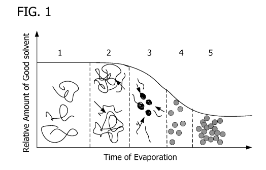
[ 0015 ] Fig. 1 is a schematic illustration of a proposed mechanism for the
formation
of a nanoparticulate dispersion.
[0016] Fig. 2 is a schematic illustration of an optical waveguide.
[ 0017 ] Fig. 3 is a schematic illustration of an optical waveguide of the
present
invention with hydrophilic and hydrophobic regions.
[0018] Fig. 4 is a schematic illustration of a liquid core waveguide of the
present
invention.
CA 02752566 2011-08-12
WO 2009/103070 PCT/US2009/034307
[0019] Figs. 5A and 5B are cross-sectional SEM images of a cross-section of a
nanoparticulate film of the present invention at different magnifications, as
described in
Example 1.
[0020] Figs. 6A and 6B are ellipsometric fitting curves for Psi and Delta,
respectively.
[0021] Fig. 7A depicts Nitrogen adsorption-desorption isotherms measured for
porous organosilicate nanoparticle networks and 7B depicts BET analysis of the
isotherms to
determine the surface area, as described in Example 2.
[0022] Fig. 8A is a t-plot analysis of the isotherms show positive Y intercept
confirming the existence of micropores in the samples described in Example 2.
The de Boer
Statistical Thickness on the x-axis is in angstroms. Fig. 8B shows pore size
distributions
determined for the sample described in Example 2.
[ 0 0 2 3 ] Fig. 9A and 9B are SEM images of the obtained nanoparticlulate
films
prepared with 14% OH content polymethylsilsesquioxane (Techneglas Corp.
GR650F), solution
aged 1 day as described in Example 3. Average particle size - l0nm
[ 0024 ] Fig. 10 is a SEM of the nanoparticulate film prepared with 2% OH
content
polymethylsilsesquioxane (Gelest, SST-3M02) as described in Example 3. The
average particle
size is about 40nm.
[0025] Figs. 11A, 11B, and 11C are TEM images of the organosilicate
nanoparticle
dispersions prepared as described in Example 4; (a) and (b) prepared with 14%
OH content
polymethylsilsesquioxane, and (c) Prepared with 2% OH content
polymethylsilsesquioxane.
Scale bar for (b) is 200nm and the scale bar for (c) is 500 nm.
[ 0 0 2 6 ] Fig. 12 is an ATR-FTIR spectra of the Hexane treated and untreated
gels aged
the same time as described in Example 5.
[0027] Fig. 13 is an ATR-FTIR spectra of the microwave treated gel as
described in
Example 5.
[ 0 0 2 8 ] Fig. 14 is a TEM image of the particles obtained from hexane
treated gel as
described in Example 5. Scale bar is 100nm.
CA 02752566 2011-08-12
WO 2009/103070 PCT/US2009/034307
6
[ 002 9 ] Figs. 15A and 15B are TEM images of the microtomed samples of the
processed gel: A, completely formed nanorod structures, and B, intermediate
structure (scale
bar = 200nm) as described in Example 6.
[ 0030 ] Fig. 16 is a schematic of the conjugation protocol of NPO and as
described in
Example 9.
[ 0031 ] Fig. 17 are photographs depicting immunofluorescences of chick heart
staining using an antibody (against laminin-1) conjugate with Rhodamine doped
nano-particles
as described in Example 9.
[ 0032 ] Fig. 18 is a time dependent decay in fluorescence of a tissue stained
with an
antibody conjugated with doped Rhodamine nanoparticles as described in Example
9.
[0033] Fig. 19 is a TEM image (scale bar = 20nm) of the rhodamine 6G Doped NPO
particles derived fom the film as described in Example 9.
[0034] Fig. 20 is a schematic depiction of a mask design for patterning
channels on
silicon substrates (Fig. 20A) and glass substrates (Fig. 20B) as described in
Example 11.
[ 0035 ] Figure 21 is a fabrication flow chart for the liquid core waveguide
as
described in Example 11.
[0036] Fig. 22 is a photograph of the experimental setup for loss
characterization of
the prototype liquid core waveguide as described in Example 11.
[0037] Fig. 23 is a photograph, illustrating the waveguiding effect using a
prototype
liquid core waveguide as described in Example 11.
[0038] Fig. 24 is a graph showing the loss characteristics for the prototype
liquid
core waveguide as described in Example 11.
[0039] Figs. 25A-25F area series of SEM micrographs of the nanoparticulate
organosilicate films obtained as described in Example 12.
[0040] Figs. 26A-26B area series of SEM micrographs of the nanoparticulate
organosilicate films obtained as described in Example 12.
[0041 ] Figs. 27A-27E are a series of graphs of thickness, refractive index
and
dielectric constant for films prepared as described in Example 12.
[0042] Figs. 28A-28E area series of graphs of thickness, refractive index and
dielectric constant for films prepared as described in Example 12.
CA 02752566 2011-08-12
WO 2009/103070 PCT/US2009/034307
7
[0043] Figs. 29A and 29B are photographs of circularly patterned photon-
emitting
films of Example 13.
[0044] Fig. 30 is TEM image of nanorods prepared in accordance with Example
14.
[0045] Figs. 31 and 32 are fluorescence intensity plots of Example 15.
DETAILED DESCRIPTION OF THE INVENTION
[0046] In accordance with one aspect of the present invention, nanoporous
films
having a relatively high surface area may be prepared. These films are crack-
resistant and may
additionally be relatively hydrophobic, exhibit an ultra-low refractive index,
and/or exhibit a low
dielectric constant. Because the films are nanoparticulate, nanoparticles
possessing unique
properties may also be derived from such films. Consequently, films of the
present invention
potentially have a wide range of uses including, for example, microbiological
applications, the
microelectronics industry, and photonics.
Nanoporous Films
[0047] In general and as described in more detail below, nanoporous films of
the
present invention are prepared by steps including but not limited to forming a
solution
containing a nanoparticle precursor in a solvent system, subjecting the
solution to a treatment
which causes nanoparticles to form from the nanoparticle precursor, depositing
the solution onto
a substrate, and curing the deposited solution to form a film. The invention
employs a liquid
dispersion of a nanoparticle precursor from which discrete nanoparticles are
formed and a
porogen in a solvent system. Other optional additives include, for example,
active
pharmaceutical agents, proteins, peptides, nucleic acids, antibodies and other
biologicals, metals
or fluorescent dyes to tailor the films or nanoparticles derived therefrom for
use in
microelectronic or bioprobe applications.
[0048] In general, the nanoparticle precursor maybe any of a range of organic
and
inorganic solids In one embodiment, for example, the nanoparticle precursor
comprises an
organo metal (or semi-metal) such as aluminum, titanium, or silicon. Exemplary
organotitanium compositions include titanium(IV) isopropoxide, titanium
tetraisopropoxide and
methyltitaniumtriisopropoxide. Examplary organoaluminum compositions include
aluminum n-
CA 02752566 2011-08-12
WO 2009/103070 PCT/US2009/034307
8
butoxide, aluminum d-butoxide, aluminum diisopropoxide ethyl acetoacetate,
aluminum
ethoxide, aluminum ethoxy ethoxy ethoxide, and aluminum isopropoxide.
[0049] In one preferred embodiment, the nanoparticle precursor is an
organosilica
material containing any of a range of materials including silicon, carbon,
oxygen and hydrogen
atoms known to those of ordinary skill. Exemplary organosilica materials
include, but are not
limited to, silsesquioxanes (RSiO1.5 where R is an organic substituent),
partially condensed
halosilanes or alkoxysilanes such as partially condensed by controlled
hydrolysis of
tetraethoxysilane, organically modified silicates having the composition RSiO3
or R2SiO2
wherein R is an organic substituent, and partially condensed orthosilicates
having Si(OR) 4 as
the monomer unit. Exemplary silsesquioxanes include alkyl silsesquioxanes such
as methyl
silsesquioxane, polymethylsilsesquioxane ("PMSSQ"), ethyl silsesquioxane,
propyl
silsesquioxane, butyl silsesquioxane and the like; aryl silsesquioxanes such
as phenyl
silsesquioxane and tolyl silsesquioxane; alkyl/aryl silsesquioxane mixtures
such as a mixture of
methyl silsesquioxane and phenyl silsesquioxane; and mixtures of alkyl
silsesquioxanes such as
methyl silsesquioxane and ethyl silsesquioxane. PMSSQ, for example, is
available from
Techneglas of Perrysburg, Ohio under the trade designation GR650F, which is in
the form of
colorless flakes.
[0050] In one embodiment, it is generally preferred that the organosilica
material be
a silsesquioxane, and more preferably hydrido silsesquioxane, methyl
silsesquioxane, ethyl
silsesquioxane, propyl silsesquioxane, iso-butyl silsesquioxane, tert-butyl
silsesquioxane, phenyl
silsesquioxane or mixtures thereof. For example, the silsesquioxanes may be
present as a
mixture including hydrido silsesquioxanes and alkyl, aryl or alkyl/aryl
silsesquioxanes. Other
exemplary silsesquioxanes include combinations of alkyl or aryl
silsesquioxanes with tetra(Ci-
C6)alkylorthosilicates such as tetraethylorthosilicate, or copolymers or
composites thereof. In
one embodiment, the silsesquioxane is hydrogen silsesquioxane or methyl
silsesquioxane and
preferably methylsilsesquioxane. In one preferred embodiment, the organosilica
is
polymethylsilsesquioxane. In one particularly preferred embodiment, the
organosilica is
polymethylsilsesquioxane having a hydroxy content of 0.5 to 20%, preferably
about 2-14%.
[00511 Typically, the silsesquioxane(s) or other organosilica materials
included in
the liquid disperson have a number average molecular weight, M, of about 5,000
to about
20,000 daltons. For example, in one embodiment, the silsesquioxane(s) or other
organosilica
materials included in the liquid disperson have a molecular weight, M,,,of
about 5,000 to about
CA 02752566 2011-08-12
WO 2009/103070 PCT/US2009/034307
9
15,000 daltons. By way of further example, in one embodiment, the organosilica
material
included in the liquid disperson is a silsesquioxane or mixture thereof having
a molecular
weight, M, of about 6,000 to about 9,000 daltons.
[0052] The organosilica (alone, or in combination with another nanoparticle
precursor) is dispersed in a solvent system. In one embodiment, the solvent
system comprises a
mixture of miscible, but different solvents, referred to herein as a first
solvent and a second
solvent. The first solvent is a "good" solvent in the sense that the
nanoparticle precursor is
relatively more soluble in this first solvent than in the second solvent. In
general, a range of
solvents or mixtures of solvents may be employed. In one embodiment, the first
solvent may be
selected from alcohols, ketones, amides, esters, or combinations thereof. For
example, one of
the first solvents may be selected from relatively low boiling point solvents
such as ethanol, 1-
methoxy-2-propanol (propylene glycol monomethyl ether), tetrahydrofuran,
acetone, 1,4-
dioxane, 1,3-dioxolane, ethyl acetate, and methyl ethyl ketone. In other
embodiments, one of
the solvents may be selected from relatively high boiling point solvents such
as
dimethylformamide, dimethylacetamide, N-methyl pyrrolidone, ethylene
carbonate, propylene
carbonate, glycerol and derivatives, naphthalene and substituted versions,
acetic acid
anyhydride, propionic acid and propionic acid anhydride, dimethyl sulfone,
benzophenone,
diphenyl sulfone, phenol, m-cresol, dimethyl sulfoxide, diphenyl ether,
terphenyl, and the like.
[0053] In one embodiment, preferred solvents for use as the first solvent
include
propylene glycol propyl ether (PGPE), 3-heptanol, 2-methyl-l-pentanol, 5-
methyl-2-hexanol, 3-
hexanol, 2-heptano, 2-hexanol, 2,3-dimethyl-3-pentanol, propylene glycol
methyl ether acetate
(PGMEA), ethylene glycol n-butyl ether, propylene glycol n-butyl ether (PGBE),
1-butoxy-2-
propanol, 2-methyl-3-pentanol, 2-methoxyethyl acetate, 2-butoxyethanol, 2-
ethoxyethyl
acetoacetate, 1-pentanol, and propylene glycol methyl ether. One particularly
preferred first
solvent for use in the solvent system is propylene glycol methyl ether
acetate. Still further
exemplary solvents include lactates, pyruvates, and diols. The solvents
enumerated above may
be used alone or in combination of two or more solvents; for example, the
solvent may comprise
one or more solvents with relatively low boiling points, i.e., boiling points
below 160 C, one or
more solvents with relatively high boiling points, i.e., boiling points above
160 C, or a mixture
of one or more solvents with relatively low boiling points and relatively high
boiling points.
[0054] To aid in the formation of the nanoparticulate nanoporous film, the
liquid
dispersion comprises a composition which is used to generate pores, sometimes
referred to as a
CA 02752566 2011-08-12
WO 2009/103070 PCT/US2009/034307
porogen. In many preferred embodiments, the second solvent (bad solvent)
functions as the
porogen, and is the same component as the second solvent (bad solvent). In
general, the
porogen has a molecular weight less than 1,500 Daltons. For example, the
porogen may be a
polymer having a molecular weight, M, of less than 1500 Daltons. In one
embodiment, the
porogen is a polymer having a molecular weight, M, of less than 1000. In one
preferred
embodiment, the porogen is a polymer having a molecular weight, M, of about
400 to about
700 Daltons. However, in the two-step process of the invention where the
porogen is not
incorporated until after formation of the nanoparticles, the molecular weight
of the porogen is
not important (may be as high as, e.g., 20,000), provided it decomposes at
elevated
temperatures.
[0055] In one preferred embodiment as noted above, the porogen may be
considered
to be a "bad" or "poor" solvent for the nanoparticle precursor. In this
embodiment, and for ease
of discussion, the porogen is referred to herein as the "second" or "bad" or
"poor" solvent and
the other solvent(s) of the solvent system in which the organosilica material
(or other
nanoparticle precursor(s)) has significantly greater solubility is referred to
herein as the "first' or
"good" solvent. In this embodiment, the first solvent can be selectively
removed from the liquid
dispersion by evaporation relative to the second solvent. As a result, when
the solvent system is
a mixed solvent system, initially containing both first and second solvents,
the organosilica
molecules are in a relatively uncoiled, i.e., an extended state. In a "good"
solvent, the chains are
extended and in a "poor" solvent on the other hand, the chain molecules assume
a highly coiled
(globule) form. See, e.g., Claudine Williams, Francoise Brochard, Harry. L
Frisch, Ann. Rev.
Phys. Chem 32,51 (1981), incorporated herein by reference. When, however, the
first solvent is
selectively removed from the mixed solvent system of the liquid dispersion,
the organosilica
molecules (or other nanoparticle precursor(s)) are induced into an
increasingly coiled or
compacted state to minimize their enthalpic interactions with the second
solvent molecules
which increase in relative concentration as the first solvent is selectively
removed from the
system. The dynamic equilibrium is thus shifted towards the formation of small
nuclei by the
selective removal of the first solvent. See, e.g., Hiroshi Yabu, Takeshi
Higuchi, Kuniharu Ijiro,
Masatsugu Shimomura, CHAOS 15, 047505, (2005), incorporated herein by
reference.
[0056] In one embodiment, any of the aforementioned solvents having a boiling
point greater than about 200 C is chosen as the porogen (or "second"
solvent). In another
embodiment, the porogen is a decomposable polymer, many types of which are
well known in
the art. See, e.g., the examples of decomposable polymers identified in U.S.
Pat. No. 5,895,263,
CA 02752566 2011-08-12
WO 2009/103070 PCT/US2009/034307
11
the entire disclosure of which is incorporated herein by reference. In one
preferred embodiment,
the porogen is a polyol. For example, the polyol may be a monomeric polyol
such as
pentaerythritol, ethylene glycol or glycerin. Alternatively, and more
preferably, the polyol is a
polymeric polyol. Preferred polymeric polyols include polyester and polyether
polyols. In one
embodiment, the porogen is a linear or branched polymer selected from the
group consisting of
polyesters, polylactides, polystyrenes substituted polystyrenes, poly-alpha
methylstyrene,
substituted poly-alpha methyl polystyrenes, aliphatic polyolefins,
polynorbornenes,
polyacrylates, polymethacrylates, and polyethers. Not all porogens function as
a second solvent.
So there are situations where the porogen and the second solvent are the same
element; and there
are situations where the porogen and the second solvent are not the same
element. Components
which have been shown to function as both a porogen and a second solvent
include PPG (MW-
424), PEG (MW-300), PEG (MW-400). Exemplary polyethers include polyethylene
oxide,
poly(propylene glycol) and polytetrahydrofuran. Poly(propylene glycol), also
known as
polypropylene oxide, is particularly preferred.
[0057] In one embodiment, the liquid dispersion contains a substantial amount
of the
porogen relative to the organosilica material (and/or other nanoparticle
precursor) and the first
solvent. For example, the liquid dispersion will typically contain between
about 30:70 and
about 70:30 parts by weight of the porogen and the organosilica (and/or other
nanoparticle
precursor), respectively. In one preferred embodiment, the liquid dispersion
will contain
between about 40:60 and about 60:40 parts by weight of the porogen and the
organosilica
(and/or other nanoparticle precursor), respectively. By way of further
example, in one
embodiment the liquid dispersion contains between about 45:55 and about 55:45
parts by weight
of the porogen and the organosilica (and/or other nanoparticle precursor),
respectively.
Similarly, the liquid dispersion will typically contain between about 10:90
and about 60:40 parts
by weight of the porogen and first solvent, respectively. In one preferred
embodiment, the
liquid dispersion contains between about 20:80 and about 50:50 parts by weight
of the porogen
and first solvent, respectively. Viewed in combination, therefore, in one
embodiment the liquid
dispersion may contain about 25:25:50 parts by weight of the organosilica
(and/or other
nanoparticle precursor), the porogen and the first solvent, respectively.
[0058] In addition to the nanoparticle precursor, the porogen, and the solvent
system,
the liquid dispersion may optionally contain various additives to tailor the
film (or particles to be
derived therefrom) for particular end-uses. For example, the liquid dispersion
may include
CA 02752566 2011-08-12
WO 2009/103070 PCT/US2009/034307
12
fluorescent dyes to be incorporated into the film (or particles to be derived
therefrom), active
pharmaceutical agents, metal nanoparticles, nucleic acids, proteins, and
peptides.
[0059] The liquid dispersions may be formed by merely combining the
nanoparticle
precursor, the porogen, the first solvent, and any other desired additives. In
a preferred
embodiment, however, the liquid dispersion is formed by combining two clear
solutions, e.g.,
solution "A" and solution "B" wherein solution "A" contains the porogen and
the first solvent in
approximately equal parts by weight of each, and solution "B" contains the
organosilica and the
first solvent in approximately equal parts by weight. Regardless of the order
of mixing, in one
preferred embodiment the liquid dispersion initially contains about 10:40:50
to about 40:10:50
parts by weight of the organosilica, porogen, and first solvent, respectively.
In addition, solution
"A" or "B" or each may be sonicated to improve the rate of dissolution. What
is formed is an
overall solution of the precursor, porogen, and other components. This
solution is then treated
to cause the formation of nanoparticles as described more fully below.
[0060] After combining, the concentration of the first solvent in the
resulting liquid
dispersion is reduced by heating and/or evaporation. The liquid dispersion may
be heated using
microwaves or by conventional, e.g., thermal, heating apparatus such as an
oven or hotplate.
Regardless of the means employed, the liquid dispersion may be heated to
reduce the
concentration of the first solvent to, for example, 9:36:45 parts by weight of
the nanoparticle
precursor, first solvent, and second solvent, respectively. Selectival removal
of the second
solvent may also be carried out (or supplemented by) vacuum evaporation which
typically
occurs, at least to some extent, when the precursor solution is deposited on a
substrate either by
spin coating or dip coating. In one embodiment, therefore, the first solvent
is selectively
removed by heating the liquid dispersion. In another, the first solvent is
selectively removed by
reducing the atmospheric pressure over the liquid dispersion. In yet another,
the liquid
dispersion is heated and the atmospheric pressure is reduced to selectively
remove the first
solvent. As noted, selective removal of the first solvent is the preferred
method of the invention;
but there are circumstances and component combinations in which nanoparticle
formation may
also be observed by simply mixing the two solutions followed by film
deposition (skipping the
evaporation step) . Advantageously, as the concentration of the first solvent
decreases, the
extent of formation of nanoparticles increases.
[0061 ] In a further alternative embodiment, the solvent system consists
entirely of a
solvent which functions as a porogen, i.e., it consists entirely of a second
solvent in which the
CA 02752566 2011-08-12
WO 2009/103070 PCT/US2009/034307
13
nanoparticle precursor particles are relatively insoluble. An example of this
approach is PMSSQ
precursor nanoparticles in PPG (Mõ 424) as the second solvent which also
functions as porogen.
This is the case when the first solvent is completely evaporated from the
system as it happens
during film deposition through spin coating or dip coating techniques.
[ 00 62 ] Without being bound to a particular theory, Fig. 1 schematically
illustrates the
inventors' expected formation mechanism for the nanoparticles employed in the
films of the
invention. At the outset, as shown in the leftmost segment 1, the liquid
dispersion is at e.g., 27
C and contains random coils of the precursor such as organosilica, e.g.,
PMSSQ. As time
passes, and the liquid dispersion is heated to e.g., 75 C to evaporate the
first solvent, the relative
concentration of the second solvent is enriched which forces the precursor
chains to assume a
globule shape, intramolecular crosslinking is initiated as shown in segment 2
as the first solvent
evaporates. This crosslinking continues during the evaporation step through
segments 2, 3, and
4, still at 75 C. And as the solution is cooled to, e.g., 27 C as shown in
segment 5, eventually
resulting in a sol-gel type of network.
[0063] In carrying out one embodiment of the invention to form the
nanoparticles,
therefore, the solution containing the precursur, first solvent, porogen, and
other components is
heated to a temperature at which the first solvent evaporates. This
temperature is selected
depending on the particular solvent system, and is, for example, at least
about 0 C, for example,
between about 0 and about 75 C. The solution is then held at that temperature
for a period of
time to achieve the desired evaporation, for example, up to about 30 minutes.
In one preferred
embodiment, where the precursor is polymethylsilsesquioxane (PMSSQ), the
porogen is
poly(propylene glycol)(Mõ 424), and the first solvent is propylene glycol
methyl ether acetate
(PGMEA), the liquid dispersion is heated to about 73 C to remove 2-40% of the
PGMEA
initially present in the liquid dispersion. So in the preferred embodiment
used herein for
illustration, as time passes, and the liquid dispersion is heated to evaporate
the PMGEA first
solvent, the relative concentration of the PPG molecules get enriched forcing
the PMSSQ chains
to assume a compact globule shape to minimize the enthalpic interactions of
the relatively
hydrophobic PMSSQ chains with the relatively hydrophilic PPG chains. The
precursor PMSSQ
molecules further undergo intramolecular crosslinking as time passes. After
cooling, the
dispersion continues to increase in viscosity and eventually gels with time,
e.g., in a period of
0.5-10 days at room temperature.
CA 02752566 2011-08-12
WO 2009/103070 PCT/US2009/034307
14
[0064] In general, the film-forming step of the invention is performed by
depositing
the liquid dispersion onto a substrate to form a film which coats the
substrate. Exemplary
substrates include, but are not limited to, ceramics, glass, metal, polymers,
or even
semiconductor materials such as single crystal silicon, polycrystalline
silicon, amorphous
silicon, silicon dioxide, silicon nitride, compound semiconductors such as
gallium arsenide, and
combinations thereof. The liquid dispersion may be applied onto the substrate
via a variety of
methods including, but not limited to, dipping, rolling, brushing, spraying,
or spin coating. As a
general proposition, the thickness of the deposited film at this point is from
about 10 (e.g., 12) to
several tens of nanometers, e.g., 50 nanometers, to several micrometers, e.g.,
2 micrometers, 3
micrometers, or greater than 3 micrometers in a single deposition. During this
deposition
operation and/or in a subsequent lower temperature operation thereafter, all
of the remaining
proportion of the first solvent evaporates.
[0065] To obtain the desired nanoparticulate porous film, after deposition of
the
dispersion, the coated substrate is typically calcined at a temperature of at
least about 200 C to
remove the porogen from the coating. In certain embodiments, the calcining
step is conducted at
two or more temperatures rather than as a controlled slow ramp or soak. The
first temperature,
typically 70 C., is to remove any first solvent remaining in the dispersion
and to further
crosslink the organosilica. In many embodiments, however, most or all of the
first solvent is
removed from the dispersion prior to film-forming and residual first solvent
is removed during
the spin-coating or other film-forming process. Advantageously, therefore, in
these
embodiments there is no need for a separate temperature hold at e.g. 70 C or
other allowance
during the calcining operation for removal of the first solvent.
[0066] In one preferred embodiment, the coated substrate is calcined at a
temperature
of at least 300 C. In another preferred embodiment, the coated substrate is
calcined at a
temperature of at least 400 C. For example, the coated substrate is calcined
at a temperature in
the range of about 450 C to about 600 C. Specific temperature and time
durations for
calcination vary depending upon the components of the dispersion, the
substrate, and the desired
pore volume. The calcination temperature of at least 200 C, 300 C, 400 C,
e.g., about 450 C to
about 600 C is to remove the porogen and to substantially, but not necessarily
completely,
crosslink the material. The calcining step is typically conducted for a time
of about 30 minutes
or less, preferably about 15 minutes or less, and more preferably about 6
minutes or less. A
slow temperature ramp rate results in densification and loss of porosity; so
it is preferred to
expose the films instantaneously to the calcination temperature, for example
using a pre-heated
CA 02752566 2011-08-12
WO 2009/103070 PCT/US2009/034307
hot plate. In this way the films at a temperature and in an environment of,
e.g., less than 100 C
are exposed instantaneously (e.g., in less than about 10 seconds) to the
calcining temperature of
at least 200 C, 300 C, 400 C, e.g., about 450 C to about 600 C.
[0067] During calcination, the porogen such as PPG essentially decomposes and
the
expanding gases offer a great increase in the translational entropy to the
PMSSQ particles. The
nanoparticles suspended in the gaseous decomposition products of PPG are in a
Brownian state
of motion with an average kinetic energy of each particle being 3/2kT. With
the existence of a
temperature gradient between the substrate and the ambient, the nanoparticles
experience a net
diffusion outward, away from the substrate The increased internal energy of
each individual
nanoparticle results in their intra-particle crosslinking, while the random
movement and
collision between the particles results in their inter-particle crosslinking
finally driving the
system to equilibrium and resulting in a porous nanoparticulate film. For this
reason, the
porosity of the films is greatly dependent on the curing/calcination
temperature. Accordingly,
the calcination is specifically performed at a temperature beyond the
decomposition temperature
of the porogen, e.g., polymer such as PPG. An increase in system entropy above
the
decomposition temperature of the porogen provides a high degree of mobility to
the
nanoparticles. Calcination may be carried out via thermal methods such as a
hot plate, oven,
furnace or the like. For thermal methods, the curing of the coated substrate
may be conducted
under controlled conditions such as atmospheric pressure using nitrogen, inert
gas, air, or other
N2/02 mixtures, vacuum, or reduced pressure having controlled oxygen
concentration.
[0068] The system employed in the invention therefore consists of functional
nanoparticles that can be thermally initiated to undergo interparticle as well
as intraparticle
crosslinking, dispersed in a thermally labile polymer layer. The behavior of
this system depends
on the calcining temperature, the temperature ramp rate, and the surface
energy of the substrate
it is deposited on. In accordance with this invention, thin films of PMSSQ
nanoparticles
dispersed in PPG result in the formation of porous films when they are
deposited on, e.g.,
hydrogen-passivated silicon substrates and subjected to instant temperature
gradients above the
decomposition temperature of PPG. In contrast, at temperatures lower than the
decomposition
temperature of PPG and therefore lower than temperatures employed in this
invention, PPG
chains play an active role in maximizing the system entropy. Segregation of
the nanoparticles
takes place at these temperatures whereby the nanoparticles lose their
translational entropy. This
loss of translational entropy of the nanoparticles is however offset by the
gain in the
conformational entropy of PPG chains as there is a far greater entropic
penalty imposed in
CA 02752566 2011-08-12
WO 2009/103070 PCT/US2009/034307
16
stretching the PPG chains around the nanoparticles to maintain a uniform
distribution. This
results in the eventual expulsion of PPG from the film resulting in a dense
film void of any
pores. As a corollary, films subjected to slow temperature ramp rates to
temperatures well
above the decomposition temperature of PPG essentially result in non-porous
films. Finally,
these films when deposited on high surface energy substrates followed by the
high temperature
treatment step results in dense, non-porous films. For example, films
deposited on freshly
piranha cleaned glass substrates and subjected to the instantaneous high
temperature
curing/calcination step resulted in the formation of dense films void of any
porosity. The
enthalpic interactions between the nanoparticles and the substrate outweigh
their translational
entropy gain resulting in the segregation of the nanoparticles to the
substrate and the eventual
formation of non-porous dense films. Accordingly, to avoid the formation of
dense films
approaching non-porous, the present invention in a preferred embodiment
employs a
combination of a relatively high temperature, high temperature ramp rate, and
lower surface
energy substrate. A preferred surface energy of the substrate lies between 32
mJ/cm2 and 48
mJ/cm2. Films deposited on lower surface energy substrates (e.g., 28 mJ/cm2)
result in
dewetting and formation of a discontinuous film.
[0069] Calcination of the coated substrate according to this invention
therefore yields
a composite of a nanoporous and nanoparticulate film on a substrate. Depending
primarily upon
the coating technique and the quantity and viscosity of the liquid dispersion
deposited onto the
substrate, the nanoporous film may have a thickness ranging from about 10
(e.g., 12) to several
tens of nanometers, e.g., 50 nanometers, to several micrometers, e.g., 2
micrometers, 3
micrometers, or greater than 3 micrometers in a single deposition. Layers
having a thickness
significantly greater than 3 micrometers could, for example, be obtained by
repeating the
operation, i.e., depositing the liquid dispersion onto a substrate to form a
coated substrate,
calcining the coated substrate to obtain a composite of a nanoporous film on a
substrate, and
repeating this sequence of steps at least once to increase the thickness of
the nanoporous film
with each successive series of steps.
[0070] In one embodiment, these methods are used to prepare nanoporous films
having pores having a mean size ranging from less than 1 nanometer to 15
nanometers, for
example of less than 10 nm. Typically, the pores have a mean size of on the
order of 4 nm with
size distribution ranging from 0.8 to 10 nanometers. In addition, the film
will have a high
degree of porosity, e.g., at least 20% of the total volume of the film is pore
volume. In one
embodiment, the porosity is greater. For example, in one embodiment, the film
has a porosity of
CA 02752566 2011-08-12
WO 2009/103070 PCT/US2009/034307
17
at least 50%. By way of further example, in one embodiment, the film has a
porosity of at least
70% by volume. All porosity values herein are by volume unless indicated
otherwise. Pore
sizes in these ranges are well below the wavelength of visible light making
these films smooth
and transparent in the visible range.
[0071 ] In general, as the porosity of the film increases, the surface area of
the film
increases and the refractive index of the film decreases, along with a
decrease in mechanical
strength. In accordance with one aspect of the present invention, nanoporous
films having a
refractive index of less than 1.33 such as less than 1.2 are obtained (as
measured at a wavelength
of 633 nm). In one preferred embodiment, the nanoporous film has a refractive
index of less
than 1.15. In another preferred embodiment, the nanoporous film has a
refractive index of less
than 1.10. Ultra low refractive index nanoporous films, i.e., films having
refractive indices of
1.048 - 1.19 are thus obtainable in accordance with the present invention.
Moreover, crack-free,
relatively thick (at least 2 micrometers), ultra low refractive index
nanoporous films may be
obtained in a single coating. Relatedly, nanoporous films of the present
invention may be
characterized by a surface area of at least 600 m2/g. In one embodiment, the
nanoporous films
have a surface area of at least 1200 m2/g, and even greater than 1400 m2/g.
[0072] The nanoporous films comprise nanoparticles, preferably organosilicate
nanoparticles, with diameter sizes that are readily tunable by selection of
liquid dispersion
components and process conditions. The percentage OH content of the
nanoparticle precursor as
well as its molecular weight determines the nanoparticle size. For example,
nanoparticles
having diameters of as little as 2 nanometers or as great as 30 nanometers may
be readily
obtained. In addition, the nanoparticles may have a relatively narrow size
distribution. For
example, 30% by weight of the nanoparticles in the film may have a diameter in
the range of 2-5
nanometers. By way of further example, 70% by weight of the nanoparticles in
the film may
have a diameter in the range of 6 - 10 nanometers. "Diameter" here loosely
refers to the largest
dimension across a particle because the particles are not strictly spherical.
[0073] As previously noted, one aspect of the present invention is nanoporous,
nanoparticulate films having relatively low dielectric constants. In general,
nanoporous,
nanoparticulate films having a dielectric constant of less than 2 may be
readily produced.
Depending upon the application, nanoporous films having even lower dielectric
constants may
be desired. Thus, one aspect of the present invention is the preparation of
nanoporous films
having a dielectric constant of less than 1.8. For example, for some
applications, it may be
CA 02752566 2011-08-12
WO 2009/103070 PCT/US2009/034307
18
desired that the nanoporous, nanoparticulate film have a dielectric constant
of less than 1.5. For
other applications, it may be desired that the film have an even lower
dielectric constant, e.g.,
1.4. The nanoporous, nanoparticulate films of the present invention can be
achieve these
objectives.
[0074 ] In addition to the organosilica nanoparticles, the nanoporous,
nanoparticulate
film may include other components to tailor the film (or nanoparticles to be
derived therefrom)
for a microelectronic, microbiologic or other application. For example, the
nanoporous,
nanoparticulate film may include a mixture of dielectric materials such as two
or more
organosilica dielectric materials or a mixture of an organosilica dielectric
matrix material with
one or more other dielectric matrix materials (e.g., an inorganic material
such as carbides,
oxides, nitrides or oxyfluorides of silicon, boron, or aluminum; or non-
organosilica organic
materials such as benzocyclobutenes, poly(aryl esters), poly(ether ketones),
polycarbonates,
polyimides, fluorinated polyimides, polynorbornenes, poly(arylene ethers),
polyaromatic
hydrocarbons, such as polynaphthalene, polyquinoxalines, poly(perfluorinated
hydrocarbons)
such as poly(tetrafluoroethylene), and polybenzoxazoles. In general, it is
preferred that when a
mixture of an organosilica material and at least one other dielectric matrix
material is used, the
organosilica material is present as a predominant component. It is further
preferred that the
organosilica dielectric matrix material in such admixtures is methyl
silsesquioxane, phenyl
silsesquioxane or mixtures thereof.
[0075] Instead of, or in addition to, a plurality of dielectric materials, the
nanoporous, nanoparticulate film may also contain a metal, a fluorescent
composition, or other
functional moiety (e.g., active pharmaceutical agents, proteins, peptides,
nucleic acids,
antibodies, and the like) to tailor the nanoporous film (or nanoparticles
derived therefrom) for
various end uses. Exemplary metals include gold, silver, platinum, palladium,
iron and cobalt.
Similarly, the fluorescent composition may be a fluorescent dye. The
fluorescent dye may be
short-lived or long-lived in fluorescent emission and further characterized by
Stokes shift, and
quantum yield. Fluorescein isothiocyanate represents a commonly used reactive
fluorescent
marker that is short-lived in emission, possesses a relatively narrow Stokes
shift, and has a
relatively high quantum yield. Rhodamine is another commonly used fluorescent
dye, which
emits at a longer wavelength than fluorescein. Lanthanide metal chelates
represent a class of
fluorescent compounds which possess a relatively large Stokes shift and are
long-lived in
fluorescent emission. This class of fluorescent molecules generally requires
another strongly
absorbing molecule to transfer the light energy to induce the strong
fluorescence. Examples of
CA 02752566 2011-08-12
WO 2009/103070 PCT/US2009/034307
19
lanthanide metals are terbium and europium which are commonly chelated by a
polydentate
chelate. Other examples of fluorescent compounds include napthalenes, pyrenes,
coumarin
derivatives, pyridyloxazole derivatives, and ruthenium complexes. As
previously noted, these
components may be conveniently incorporated into the nanoporous film by adding
them to the
liquid dispersion from which the nanoporous film is derived.
[00761 Depending upon the application, the nanoporous, nanoparticulate film
may
be relatively more hydrophilic, relatively more hydrophobic or intermediate of
the two. In
general, the degree of hydrophilicity may be determined by the contact angle
of a droplet of
water with contact angles of at least 90 generally being regarded as
hydrophobic and contact
angles of less than 90 generally being regarded as hydrophilic. The degree of
hydrophilicity
may be controlled, at least in part initially, by selection of organosilica
materials. In general,
those with greater hydroxyl content and less alkyl substitution tend to be
more hydrophilic and
those with less hydroxyl content and more alkyl substitution tend to be more
hydrophobic. In
addition, the nanoporous, nanoparticulate films may be rendered more
hydrophilic by surface
oxidation to introduce silanol groups. One such approach is by exposure to
oxygen plasma. In
one embodiment, therefore, a droplet of water on the nanoporous film will have
a contact angle
of less than 90 . For example, in one embodiment the contact angle may be less
than 60 . In a
further embodiment, the contact angle may be less than 30 . In a still further
embodiment, the
contact angle may be less than 20 such as, for example, 10 . A significant
advantage in
comparison to many prior art films is that the films of the invention can be
made to be inherently
hydrophobic. In many applications this can be critical to avoiding uptake of
water during
processing, handling, and storage. Moreover, hydrophilicity can be easily
imparted to these
hydrophobic films shortly prior to their incorporation into, for example,
biological applications
where hydrophilicity may be required.
Nanoparticles
[0077] In one aspect the present invention is directed to nanoparticles having
diameters of as little as 2 nanometers or as great as 30 nanometers. The
particles may be in form
of nanorods, e.g., nanoparticles having a length to diameter (aspect ratio) of
at least 2:1, or as
particles having an aspect ratio in which the greatest dimension is less than
twice the smallest
dimension, such as roughly sphere-like shapes. Regardless of aspect ratio, the
nanoparticles
may have a relatively narrow size distribution. For example, 30% by weight of
the nanoparticles
CA 02752566 2011-08-12
WO 2009/103070 PCT/US2009/034307
may have a diameter in the range of 2-5 nanometers. By way of further example,
70% by
weight of the nanoparticles may have a diameter in the range of 6 - 10
nanometers.
[0078] The nanoparticles maybe derived from the nanoporous, nanoparticulate
films
of the present invention, by mechanically or acoustically fracturing the
nanoporous,
nanoparticulate film, for example, by scraping or sonication, or scraping
followed by sonication
in a suitable solvent.
[0079] Alternatively, nanoparticles maybe obtained directly from the solution
phase
by precipitation, e.g., by addition of a solvent mixture of water and ethanol
in the presence of
suitable surfactants. Alternatively, the nanoparticles may be obtained by
spray pyrolisis as
described, for example, in U.S. Patent No. 7,276,224. When organosilanes are
used as the
nanoparticle precursor, particle size may be controlled, in part, by treating
the organosilane with
a silane coupling agent, for example, trimethyl chlorosilane (TMCS), octadecyl
trichlorosilane
(OTS) or the like, which will reduce the degree of interparticle crosslinking.
[0080] In addition to obtaining hydrophobic nanoparticles directly from the
nanoporous, nanoparticulate films through scraping, hydrophobic nanoparticles
can be directly
precipitated from the nanoparticulate precursor solution in bulk quantities.
Nanoparticulate
precursor solution is prepared as described above. The wt% of porogen such as
PPG is kept at
50% with respect to the precursor such as PMSSQ, and, for example, PMA is
chosen as the
good solvent. In one embodiment, the precursor solution is heated at 70 C for
20 minutes under
stirring to allow the formed PMSSQ nanoparticles to crosslink.
[0081 ] In carrying out this direct formation method, the precursor solution
(e.g., 1
mL) following the evaporation step is diluted (e.g., to 10 ml in ethanol). The
silane coupling
agent (e.g., 150 microliter TMCS) is added dropwise to this solution and the
solution is vortexed
to facilitate uniform reaction of the coupling agent with the dispersed
nanoparticles in the
solution. The coupling agent is allowed to react with nanoparticles for a
period of one hour
during which the initially clear solution turns milky. TMCS basically reacts
with the surface -
OH groups present on the PMSSQ nanoparticles making them further hydrophobic
resulting in
their eventual precipitation from the ethanol. These nanoparticles can be
recovered in the form
of a gelatanious precipitate through centrifugation and decantation of the
supernatant solution.
The obtained nanoparticles are then dried using nitrogen flow and can be
easily dispersed in any
non-polar solvent like toluene, chloroform, etc. Using this approach bulk
quantities of these
nanoparticles can be obtained that can be easily dissolved in various non-
polar solvents at
CA 02752566 2011-08-12
WO 2009/103070 PCT/US2009/034307
21
relatively high loadings (50-60%). The particle size ranges, for example, from
about 2 to about
nm, with a mean particle size of, for example, 3.5 nm.
[0082] The nanoparticles of the invention have a relatively large surface
area. In
general, the free-flowing nanoparticles have a surface area of at least 500
m2/g. In one
embodiment, the free-flowing nanoparticles have a surface area of at least 600
m2/g. For
example, the free-flowing nanoparticles may have a surface area of at least
1,000 m2/g. In one
preferred embodiment, the free-flowing nanoparticles have a surface area of
about 500 to about
1700 m2/g.
[0083] As previously described, the nanoporous films may contain various
components to tailor the film for a microelectronic, microbiologic or other
application. Because
the free-flowing nanoparticles are obtained directly from the nanoporous,
nanoparticulate film,
the free-flowing nanoparticles may also contain any of the aforementioned
metals, dielectrics,
dyes, etc. to tailor the nanoparticles for use in a microelectronic,
microbiologic or other
application.
Liquid Core Waveguides
[0084] Light waveguides are structures used to guide light from one point in
space to
another with minimal losses. The most common design for the waveguides shown
schematically in Fig. 2 consists of a dielectric material with high refractive
index (core 20)
surrounded by a material of lower index of refraction (cladding 22). Light is
guided in the core
20 between the waveguide's inlet and outlet by means of total internal
reflection. The refractive
index contrast between the core 20 and the cladding 22 determines the
acceptance angle cone 24
for the light beam. Rays that approach the waveguide with angles within the
acceptance cone 24
are guided through the waveguide, while those with angles greater than the
acceptance cone 24
are reflected as shown in Fig. 2.
[0085] While most of the light waveguides feature a solid core, having an
aqueous
medium as the core has its added advantages. Research and development of
highly target-
specific sensors has attained a level of paramount importance because of the
burgeoning need
for applications in national security, health care, the environment, energy,
food safety, and
manufacturing. Fluorescence-based sensing is among the most commonly used
transduction
methods. These sensors utilize fluorescent dye molecules as probes and most
sensing
applications are performed in aqueous solutions. Since the refractive index of
water (1.33) is
CA 02752566 2011-08-12
WO 2009/103070 PCT/US2009/034307
22
lower than most solid-state materials, the excitation of the dye and
collection of fluorescence are
typically performed through either bulk optics such as epifluorescence
microscopes or
evanescent coupling in solid waveguides. These two configurations impose a
number of
limitations. For example, in evanescent coupling, efficiency of excitation and
fluorescence
collection is poor, resulting in low signal-to-noise ratio and sensitivity.
Bulk optics adds
additional cost and makes it difficult to multiplex sensors on a larger scale.
In addition to this,
liquid core waveguides can also be applied for use in absorbance spectroscopy
and Raman
spectroscopy. In Raman spectroscopy, confinement of light in the liquid core
improves the
efficiency of Raman generation. In addition, a combination of Surface enhanced
Raman
spectroscopy (for example, by deposition of gold nanoparticles on the
nanoporous film surface)
with the waveguide design will result in even higher Raman signal
sensitivities.
[ 0 0 8 6 ] As the refractive index of water is 1.3 3 which is lower than most
readily
available materials, construction of a liquid core waveguide with an aqueous
core becomes a
challenge. Teflon AF 1600 (n - 1.31) and Teflon AF 2400 (n - 1.29) have long
been the only
materials reported on being used as the cladding material for such waveguides.
These materials
however are not the ideal choice for these waveguides, especially in
applications for use as a bio
or a Raman based chemical sensor. Teflon offers little chance for chemical
functionalization
desired in most biosensing applications. The refractive index contrast between
Teflon and water
is at most 0.04 which translates to an acceptance cone of just 18 degrees. For
applications in
biosensors and Raman based chemical sensors, this poses a significant
limitation. As the
fluorescence is generated in all directions within the waveguide, it is
advantageous for the
waveguide to have a large acceptance cone thus guiding most of the generated
fluorescence
through the length of the waveguide.
[0087] Air has the lowest refractive index among all materials (refractive
index of
1.0). Incorporating air as the cladding material would yield a waveguide with
an ultra high
numerical aperture. However, designing an air-clad liquid core waveguide
system would be a
challenge. Thus for a more efficient liquid core waveguide bio/chemical
sensor, new materials
with ultra low refractive indices have to be engineered. Nanoporous,
nanoparticulate dielectrics
such as in accordance with this invention are therefore an ideal choice as the
cladding material.
With pores in the order of 2 - 4 nm diameters, these materials have an
extremely low refractive
index. In one embodiment, refractive indices of 1.15 or less are achieved
which correspond to
an acceptance cone of at least 42 degrees. These dielectric materials have
excellent adhesion to
the common substrates and easy functionalization of these surfaces with well
established
CA 02752566 2011-08-12
WO 2009/103070 PCT/US2009/034307
23
methods makes them all the more attractive for biosensor applications. The
large refractive
index contrast between the aqueous medium (1.33) and the nanoporous dielectric
film (1.10-
1.13) results in a large acceptance cone as compared to Teflon AF (1.29). Thus
shorter channels
can be used in applications such as Raman based sensors and fluorescence based
biosensors.
[0088] Surface modification of these films can be performed by well
established
processes, unlike Teflon AF based materials, which is an important requirement
in biosensor
design. A further attractive aspect of the invention with respect to
biosensors is the rapid
formation of ultra-low refractive index, low stress, crack free and smooth
films based on
organosilicate. The fabrication methodology of these nanoporous dielectric
films makes them
readily amenable to mass production methodologies. In one embodiment, the as-
formed films
are highly hydrophobic thus no further treatments are necessary to avoid water
seepage into the
pores and the eventual degradation of the films.
[0089] One aspect of the present invention, therefore, is a compact,
microfabricated
chip based liquid core waveguide (LCW) system employing nanoporous dielectric
coatings as
the cladding material. Conventional microfabrication of liquid core waveguides
involves
etching channels in silicon/glass followed by coating of a low refractive
index dielectric material
and subsequent bonding with a similarly processed glass substrate. Integration
of these
nanoengineered materials in the liquid core waveguide design is a challenge.
Unlike Teflon
where thick films could be formed within the etched channels, forming thick
nanoporous
organosilicate coatings results in a largely stressed film which eventually
cracks. To circumvent
these issues, a modification has been done in the basic design of the liquid
core waveguides in
which the sidewalls are eliminated. The new design of device 30 in Figs. 3 and
4 relies on
interaction of water with patterned hydrophobic regions 32 and hydrophilic
regions 34 on
substrates 36. The patterned hyrdrophobic and hydrophilic regions are the
nanoporous,
nanoparticulate films of the invention having a refractive index of, e.g.,
1.10. In this design, a
substrate is patterned such that it consists of super hydrophilic channels 44
(e.g., water contact
angles of <20 degrees) separated by super hydrophobic regions 42 (e.g., water
contact angles of
>90 degrees). Such a layout forces water 38 to be confined within the
hydrophilic 44 regions of
the substrate. Two such substrates 36 are patterned and held on top of each
other with some
spacers 40 of, e.g., teflon in between.
[0090] As shown in Figs. 3 and 4, when water 38 is introduced at one end of
the
channel by placing a drop, the hydrostatic force together with the surface
tension of the
CA 02752566 2011-08-12
WO 2009/103070 PCT/US2009/034307
24
hydrophilic top and bottom surfaces suck the water to fill the hydrophilic
channels 44. The
hydrophilic channel 44 in Fig. 4 separates two hydrophobic regions 42, all
being between the
spacers 40. The hydrophilic channel 44 contains the water with a refractive
index of 1.33; the
hydrophobic channels 42 contain air with a refractive index of 1.0; and the
hydrophobic regions
32 and hydrophilic regions 34 on substrates, being formed from the nanoporous
films of the
invention, have a refractive index of, e.g., 1.1. Water that is present at the
hydrophobic end
experiences a force in the opposite direction due to surface tension. As long
as this force is
larger than the hydrostatic force that is acting to push the water in, the
water will not be able to
enter the hydrophobic regions. Thus, it is possible to confine the water 38
only in the
hydrophilic channels by this design, in effect having a column of water that
can serve as a
waveguide. Figure 3 shows two hydrophilic channels defined by the hydrophilic
regions 34; but
for ease of illustration, Fig. 4 shows just one hydrophilic region 44.
Optical Fiber Waveguides
[0091] High numerical aperture (NA) optical fibers are increasingly becoming
attractive for medical illumination applications as they provide for broad
irradiation patterns
enabling the use of small diameter fibers for minimally invasive surgeries.
Apart from
minimizing the modifications needed to disperse output patterns, these fibers
allow lower bend
radius without introducing significant losses due to large bends. The power
requirements of the
lamp source are also greatly reduced as the high acceptance angle associated
with these fibers
accepts greater percentage of light compared to a low NA optical fiber.
[0092] Conventional optical fibers, although designed to be low loss, suffer
from
having low numerical apertures. Increasing the refractive index contrast
between the core and
cladding of the optical fiber increases its numerical aperture. This can be
accomplished by
choosing materials with very low refractive indices to function as the
cladding material.
However, most of the readily available solid state materials have relatively
high refractive
indices. Nanoporous dielectric coatings offer a unique opportunity to address
this issue.
Refractive indices as low as 1.10 (compared to 1.46 of a typical cladding
material) can be
obtained by packing different volume ratios of air pockets in the matrix
material. However,
adapting these coatings to the fiber optics is challenging. Existing
fabrication processes to obtain
these coatings are usually time consuming and require tight heating/cooling
cycles making it
difficult and uneconomical for practical application.
CA 02752566 2011-08-12
WO 2009/103070 PCT/US2009/034307
[0093] One challenge is that once the coatings have been applied on the
substrates, in
order to obtain crack-free porous films, extremely slow temperature ramp-
up/ramp-down times
(of the order 1 C/min) are used. This places a serious constraint on the
adaptability of these
coatings for optical fiber manufacture especially while integrating it with
the conventional
optical fiber manufacturing techniques.
[0094 ] Another challenge associated with these coatings is stability to
thermal
shocks. Beyond a certain thickness (-1 micron) the films are extremely
susceptible to cracking
introduced due to thermal stresses. Optical coatings > 1 micron thickness are
usually required
for waveguide applications to confine most of the propagation modes within the
fiber core.
[0095] Accordingly, nanoporous, nanoparticulate coatings of the present
invention
are ideal for this application. Apart from rapid formation of these films,
with an annealing time
typically between about 3 and about 5 minutes after film deposition, these
films are stable to
temperature shocks resulting from the fast heating and cooling cycles for
curing/calcinations
process. The obtained coatings are hydrophobic in nature and thereby resist
moisture absorption
and subsequent film degradation. Furthermore, the chemical precursors required
for the
preparation of these films are inexpensive, making this an economical solution
to produce high
numerical aperture optical fibers compared to other methods. These coatings
can be directly
adapted with the traditional fiber optic manufacturing techniques to yield
optical fibers with high
numerical apertures.
[0096] It is therefore seen that fiber optics with silica core and
organosilicate thin
film as cladding has large acceptance angle and thus these optical fibers can
be used for
applications needing large numerical apertures to collect the maximum light
possible. Such
optical fibers find use in medical illumination applications. Numerical
apertures as large as 0.9
can be achieved with the use of such coatings as cladding.
High Surface Area Substrates for Chemical-Biological Assays
[0097] The high surface area associated with the nanoporous, nanoparticulate
films
of the invention can be utilized for chemical-biological assays for increased
density of binding
to enhance sensitivity. Because of the nanoparticulate nature of the film
together with the
presence of nanopores, these films feature a high surface area (e.g., >500
m2/g), thus enabling
for a greater density of immobilization of biological probes and thereby
enhancing the
sensitivity. The large surface area can be used for chemical and biological
sensor platform to
CA 02752566 2011-08-12
WO 2009/103070 PCT/US2009/034307
26
enhance the detection sensitivity. Also, organosilicate particle surface can
be easily modified to
provide chemically-accessible hydroxy groups (e.g., by oxygen plasma or ozone
treatment) for
bonding with biological molecules. Advantageously, these films are transparent
over the visible
spectra and provide a greater density of immobilization, translating into a
higher signal to noise
ratio, for example, in fluorescence based biosensing.
Imaging
[0098] The formation mechanism of the films and nanoparticles can be
controlled to
incorporate fluorescent dyes, metal nanoparticles intercalated within the
organosilicate
nanoparticles, as discussed above. Fluorescent dielectric nanoparticles, for
example, are
biocompatible, thus enabling their use for in vivo imaging applications.
[0099] In this application, dye-doped nanoparticles are formed in a mixed
solution of
good and bad solvent. There are two ways to extract the nanoparticles as
discussed above, one of
which is precipitation from the solution, and the other of which is by making
a thin film of the
solution. In the first method, nanoparticles formed in solution are collected
by centrifuge. In the
second, more preferable method, there is thin film formation since it provides
freedom for
surface modification by plasma treatment, which is an essential step to create
carboxyl or amine
groups on the surface of the nanoparticles for biological applications, while
dye-doped
nanoparticles have methyl group on surface. Once a thin film is obtained by,
e.g., spin coating, it
is annealed at high temperature depending upon the dye bond in the particle to
remove free dye
on the surfaces of nanoparticles and enhance crosslinking of nanoparticles. In
this annealing
step, the role of the porogen (bad solvent) is crucial for preventing inter
crosslinking among
nanoparticles. For rhodamine 6G doped nanoparticles, 250 C, for example, is
optimal. The
annealed films are then treated with plasma to render the nanoparticle
surfaces hydrophilic so as
to disperse the particles in water for biocompatibility. Oxygen plasma is used
to create carboxyl
groups for the nanoaprticles. For example, ATR spectra have shown COOH groups
at 1720 cm-
1 after oxygen plasma treatment. Other plasmas such as ammonia, nitrogen and
carbon dioxide
plasmas are used for other purposes. The plasma treated films are then scraped
and dispersed in
water. The size of nanoparticles may vary, for example, from 3 nm to 10 nm as
demonstrated by
TEM imaging, depending upon -OH contents in the PMSSQ. The dye-doped
nanoparticles from
this synthesis are very photostable. The reason is that the dyes trapped
inside particles
(hydrophobic core) have an outside protection layer (hydrophilic shell). The
hydrophobic
CA 02752566 2011-08-12
WO 2009/103070 PCT/US2009/034307
27
core/hydrophilic shell structure is due to hydrophobic nature of PMSSQ and
carboxyl group on
surface after oxygen plasma. Photobleaching of R6G-doped nanoparticles and
pure R6G
nanoparticles at an emission wavelength of 581 nm has shown high
photostability after 30
minutes continuous exposure to 10x lens under 130W mercury lamp.
Other Applications
[00100] Inasmuch as one aspect of the present invention is a process for the
rapid
formation of ultra-low refractive index, low stress, crack free and smooth
films based on
organosilicate, the method, films, and nanoparticles have application
elsewhere where its
features such as high porosity, low refractive index, and the like are
applicable. The fabrication
methodology of these nanoporous dielectric films makes them readily amenable
to mass
production methodologies. As noted, the as-formed films are highly hydrophobic
thus no
further treatments are necessary to avoid water seepage into the pores and the
eventual
degradation of the films. For example, these films can also be applied for use
as low - k
dielectrics in semiconductor industry for silicon microchip technology, as
well as, organic thin
film transistors. They also have thin film laser application. In nanorod form,
the nanoparticles
may be used as bioscaffold material for tissue repair.
[ 0 0101 ] The following examples illustrate the invention.
Example 1
[00102] For the preparation of films, polymethylsilsesquioxane (PMSSQ) having
a
molecular weight, M, of 6000 - 9000 (Techneglas; Perrysburg, Ohio; Gelest,
Inc; Mossisville,
PA), poly(propylene glycol) (PPG) having a molecular weight, M, of 424 (Sigma-
Aldrich; St.
Louis, MO) and propylene glycol methyl ether acetate (PGMEA) (Sigma-Aldrich;
St. Louis,
MO) were used as supplied. A 50 % by weight solution of PMSSQ was prepared by
dissolving
5g of PMSSQ in 5 g of PGMEA and designated as solution A. This solution was
then filtered
using a 0.25 micron filter. A 50 % by weight solution of PPG was prepared in
PGMEA by
dissolving 5 g of PPG in 5 g of PGMEA and designated as solution B. Solutions
A and B were
then sonicated separately for at least 10 - 15 minutes to ensure complete
dissolution of the
respective solutes. After obtaining clear solutions, Solution A was mixed with
solution B and
CA 02752566 2011-08-12
WO 2009/103070 PCT/US2009/034307
28
sonicated for an additional 5 minutes to obtain a homogenous solution. This
solution was then
taken in an open beaker and placed on a hot plate at 70 C under constant
stirring (600 rpm).
The weight of the solution was continuously monitored and the solution was
removed from the
hot plate after a predetermined amount (0.5g, lg, 2g and 6g) of the PGMEA was
evaporated.
The resulting clear, viscous solution was then transferred into a glass bottle
and sealed for
further use.
[00103] This dispersion was then spin cast onto silicon substrates to form
thin films (2
micron thickness). Immediately after the spin coating, the films were
calcinated on a hot plate at
470 C for 5 minutes for PPG burn out resulting in the nanoporous film. In
addition to serving
as a poor solvent, the PPG molecules act as a plasticizer during the final
film formation resulting
in a low stress, crack free film. The obtained films could withstand the large
thermal stresses
resulting from instantly stepping down to room temperature from 470 C.
Figures 5A and 5B
show the crosssectional SEM of the film along with the magnified view. From
the figure it can
be seen that the film is smooth and is comprised of nanoparticles with a
narrow size distribution
in the range 2-3 nm. It can also be seen that it is possible to control the
size of the nanoparticles
by using different Si-OH content PMSSQ varying the initial compositions of the
solution,
amount of the solvent evaporated, and the temperature at which the evaporation
is carried out.
[ 00104 ] Electrical characterization of these films has been performed in a
probe
station on the metal/insulator/metal (MIM) structures at room temperature.
Capacitance-voltage
(C-V) measurements were carried out using an HP 4284A LCR meter at frequencies
100 kHz
and 1 MHz. Nanoporous dielectric films were deposited on heavily doped,
electrically
conductive silicon substrates from one day aged solution. Aluminum dots were
then sputter
coated on these films through a shadow mask. Dielectric constant measurements
performed in
this manner gave a value of 1.4 at 100 KHz and 1.42 at 1MHz. Optical
characterization of these
films was carried out by variable angle spectroscopic ellipsometry (VASETM,
J.A Wollam, Inc.).
Ellipsometric measurements were taken on the porous films at 65 and 75
incident angles with
wavelength scans performed from 300nm to 1700nm. For the data modeling, Cauchy
model
with non-idealities was used to fit the data. The details of the modeling of
nanoporous
organosilicate films are described in M. T. Othman, J. A. Lubguban, A. A.
Lubguban, S.
Gangopadhyay, R. D. Miller, W. Volksen, H.-C. Kim,, J. Appl. Phys. 99, 083503
(2006). The
porosity of the films has been modeled using the Maxwell Garnet Effective
medium
approximation model which gave a porosity of about 70% for these films.
Refractive index
measurements of the films gave a value of 1.10 with a thickness of 884 nm.
Figures 6A and 6B
CA 02752566 2011-08-12
WO 2009/103070 PCT/US2009/034307
29
show the fitting curve as well as the depth profile of the film from the
graded Cauchy and non
ideal model fit.
[00105] Nanoindentation technique (Tribolndenter, Hysitron Inc.,) was used to
study
the mechanical properties of the film. From the nanoindentation measurements,
the modulus of
elasticity of the film has been calculated to be 0.56 GPa. It is well
documented that the modulus
of the nanoporous films drop rapidly with increasing porosity. Thus in
comparison to the
nanoporous dielectric films prepared by the porogen approach of the same
porosity (70%) these
films are higher in modulus and expected to be more robust. Apart from the
good thermal
stability (up to 500 C) these films have shown to have good adhesion to
common substrates
(Silicon and Pyrex glass). Thus, these films can be used as low-k material in
Silicon back-end
process as well as a gate dielectric for thin film transistors. Such low-k
materials are
increasingly becoming attractive for use as dielectrics in organic field
effect transistors.
Example 2
Physical Characteristics
[00106] Nitrogen adsorption-desorption isotherms for samples prepared as
described
in Example 1 were analyzed using a Quantachrome Autosorb-1 automated gas
sorption system
and the surface areas of the samples were computed using BET method. For the
analysis, films
were prepared on silicon substrates from one day aged solutions. The
nanoparticulate powder
was obtained by carefully scraping the film from the substrate. Since the
samples are
hydrophobic, these were degassed at room temperature for twelve hours. The
isotherms obtained
for these films shown in Fig. 7A are classified as Type IV, as normally
observed in typical
mesoporous samples (pore size of 2-50 nm as defined by IUPAC). However, it is
seen that that
there is a sharp increase of the volume of nitrogen adsorbed at relative
pressures (P/P ) in the
range of 10-'-10-4. Therefore, it is expected that these samples are likely to
exhibit both
microporosity and mesoporosity.
[00107] The BET plots shown in Fig. 7B reveal that the surface area of these
nanoparticulate porous films prepared using PMSSQ precursor with 2% and 14% OH
content
are 657m2/g and 1325m2/g respectively. The high surface area of these samples
is attributed to
the large amount of pores created by the removal of PPG, voids between the
nanoparticles and
extremely small size of these nanoparticles with a narrow size distribution.
Smaller
nanoparticles with the size range of 10-14 nm were observed in films prepared
using PMSSQ
CA 02752566 2011-08-12
WO 2009/103070 PCT/US2009/034307
precursor with 14% OH content in comparison with that of 20-40 nm sized
particles observed in
films prepared with 2% OH content.
[ 00108 ] High surface area porous silica materials reported in the literature
are
conventionally hydrophilic and therefore those samples require post-treatments
with silylating
agents like TMCS, HMDS etc. In contrast, the process of the present invention
yields high
surface area, hydrophobic porous silica nanoparticles in a single step
synthesis procedure.
[00109] T-plot analysis of the isotherms was performed to determine the amount
of
microporosity in the samples. T-plots shown in Fig. 8A reveal positive Y-axis
intercept for both
these samples. The de Boer Statistical Thickness on the x-axis is in
angstroms. The obtained
micropore volumes for films prepared using precursors with 2% and 14% OH
content are
0.03cc/g and 0.006 cc/g respectively. The microporosity in these samples
constitutes 2.3 % and
0.4 % of the total pore volume observed. For the sample prepared with 2% OH
content in
MSSQ precursor, the micropore surface area of 80m2/g and the external surface
area of 577m2/g
add up to 657 m2/g which equals the BET surface area. Similarly, for the
sample prepared with
14% OH content in MSSQ precursor, the micropore surface area of 42m2/g and the
external
surface area of 1273m2/g add up to 1315 m2/g, which is very close to the total
surface area of
1325 m2/g obtained from BET analysis.
[00110] Pore size distribution was determined applying the density functional
theory
and Monte Carlo simulation methods using the AS 1 WIN software package. The
pore size
distributions (Fig. 8B) reveal that the micropore mode is about 1.5 nm for
both the samples. The
size distribution of mesopores lies in the range of 3-9 nm in case of smaller
nanoparticles (10-14
nm) prepared with 14% OH content in PMSSQ precursor and it lies in the range
of 3-16 nm in
case of larger nanoparticles (20-40 nm). The total pore volume obtained for
samples prepared
with 2% and 14% OH content in MSSQ precursor are 1.32 cc/g and 1.5 cc/g
respectively. The
large amount of porosity exhibited these organosilicate hydrophobic films is
attributed to the
removal of PPG and the voids formation arising from the assembling of the
nanoparticles on the
substrate at the time of film deposition.
CA 02752566 2011-08-12
WO 2009/103070 PCT/US2009/034307
31
Example 3
Nanoparticulate Films
[ 00111 ] Nanoparticulate films were prepared by spin deposition onto freshly
1:10
HF:DI dipped silicon substrates followed by a heat treatment step of 400 C for
5 minutes, using
the procedures described in Example 1 except as otherwise noted. These films
were prepared
with 14% OH content PMSSQ from Techneglas Inc, (GR650F). The films were
prepared with
one day aged solution. Figs. 9A and 9B depict the SEM of the film's cross
section. The films
prepared from 2% OH content PMSSQ (Gelest, SST-3M02), on the other hand, gave
nanoparticulate films with particle sizes - 40 nm (see Fig. 7). The difference
in particle size
between the 14% (Mw 5000) and the 2% PMSSQ (7000-8000) may be due to the
differences in
molecular weight between the two different PMSSQ. 2% OH content solutions tend
to take
longer time to gel because of the presence of less number of reactive sites.
Example 4
Nanoparticulate Dispersions
[ 00112 ] A dispersion of organosilicate nanoparticles was prepared by
scraping a film
prepared as described in Example 1 with a flat razor blade, collecting the
resulting fine powder
and dispersing it in a surfactant solution via sonication. The resulting
solution was then filtered
with a 0.2 micron filter to obtain a clear nanoparticle dispersion. Figures
10A, 10B, and 10C are
TEM images of the resulting organosilicate nanoparticle dispersions. The scale
bars are 1
micron, 200 nm, and 500 nm, respectively in A, B, and C.
Example 5
[00113] Nanoparticles were obtained directly from a gel prepared as set forth
in
Example 1 except that the gel was treated with n-hexane. n-Hexane treatment of
the gel results
in an effective dehydration of the gel thereby freezing the crosslinking
reactions occurring
within the gel. Solutions were poured into glass Petri dishes and allowed to
gel. The gels were
later soaked in hexane for a 12 hour period following which excess Hexane was
decanted.
Figure 12 shows the ATR-FTIR spectra of the hexane-treated and not treated-
gels aged the same
time.
CA 02752566 2011-08-12
WO 2009/103070 PCT/US2009/034307
32
[ 00114 ] Although the gels were aged the same time, in the case of the hexane
treated
gel, the extent of cross linking (evident from the twin peaks in the region
1100-1000 /cm) is
considerably reduced. Also, regular gels crack over time as the gel shrinks,
oozing out the
solvent and PPG in the process and gets densified. This was not observed in
the case of the
hexane treated gel.
[00115] In order to cross link the particles fully before extracting them from
the gel,
the gel was placed in a conventional microwave oven and microwaved for 5
minutes.
Microwaving regular gels under similar conditions results in a phase
separation between the
liquid and the solid parts; this appears to be due to the accelerated
interparticle crosslinking
within the gel. However, this behavior was not observed for the hexane treated
gels suggesting
that the microwave treatment resulted in the intra particle crosslinking while
the particles
remained separated from each other. No cracking of the gel was observed even
after the
microwave treatment. Figure 13 shows the ATR-FTIR spectra of the microwave-
treated gel.
[ 0 0 116 ] Extraction of the particles from the gel was accomplished by
crushing and
grinding the microwave treated gel and dissolving the resultant white powder
in surfactant
solution. The solution was filtered with a 0.2 micron filter to obtain a clear
dispersion. Fig. 14
gives the TEM of the obtained particles, with the scale bar being 100 nm. As
can be seen from
the TEM, there are bigger particles possibly due to agglomeration as well as
smaller particles
l0nm (same size as obtained from films).
Example 6
Organosilicate Nanorod Networks
Nanoporous Organosilicate Nanorods
[ 00117 ] It has been observed that aging of the nanoporous organosilicate
precursor
solutions at ambient conditions results in the formation of gel with time. The
gelation occurs
within 7 days time and is strongly dependant on the amount of the evaporated
solvent as well as
the amount of -OH content in the PMSSQ starting material. Greater the amount
evaporated,
quicker the solution gels. Increased -OH content in the PMSSQ starting
material results in a
quicker gelling precursor solution. The gels have been dried to remove all the
solvents and
washed and filtered with ethanol to remove most of the PPG. These gels are
later subjected to
calcinations to result in a fine white powdery substance. When examined under
a TEM, it has
CA 02752566 2011-08-12
WO 2009/103070 PCT/US2009/034307
33
been observed that the white substance consists of a network of nanorods which
can be
separated if sonicated in a suspension.
[ 00118 ] Nanorods and nanorod networks can be obtained from the gels by aging
the
gels sufficiently to let the nanoparticles come together and form networks.
The gels are crushed
and washed repeatedly with ethanol to remove excess PPG and calcined to remove
the PPG and
fully crosslink the network. The obtained powders are later sent for
microtoming to be observed
in TEM. Figure 15 gives the TEM of the microtomed samples. Figure 15A (scale
bar = 500nm)
is from a dense gel aged for a long time while 15B (scale bar = 200nm) is from
a fresh gel.
Example 7
Substrate Surface Dependant Properties of the Films
Plasma Treatment of Nanoporous Silicate Films
[ 00119 ] Low power oxygen plasma treatment of a primary nanoporous
organosilicate
film followed by deposition of a secondary organosilicate film has been found
to collapse the
pores of the secondary coating. In a typical process, a thinner film of the
primary coating is
applied first and heat trated to 470 C for 2 minutes. This film is later
treated to a low power
oxygen plasma treatment and immediately a secondary nanoporous organosilicate
film (thicker
film, no dilution) is spin coated over the primary film and processed at 470
C for 5 minutes. It
has been noted that the dielectric properties of the nanoporous silicate films
for the films
prepared on plasma treated nanoporous silicate surfaces is altered. The
refractive index of the
films has been found to increase to the inherent refractive index of the
organosilicate films
suggestive of the collapse of the pores.
[ 0 012 0 ] Table gives the refractive index and thickness values of films
prepared by
normal deposition process and on plasma treated nanoporous silicate surface.
The hydroxy
groups on the substrate surface have been shown to have an effect on the
dielectric as well as the
optical properties of the final film.
Table 1
Refractive index and thickness of films with and without adhesion layer
Sample Adhesion Annealing Thickness Refractive
layer conditions index
CA 02752566 2011-08-12
WO 2009/103070 PCT/US2009/034307
34
1 No Hot plate 760 nm 1.149
470 C
mins
2 Yes Hotplate 1150 nm 1.37
470 C
5 mins
Adhesion Hot plate 201 nm 1.38
layer 470 C
5 mins
[00121] Similarly, the coatings on glass substrates have been shown to yield
films
with properties different from those deposited on silicon substrates. Films
deposited on piranha
treated glass substrates have been shown to exhibit higher refractive indices
than films deposited
on glass substrates cleaned with organic wash.
Example 8
Dye Incorporated Organosilicate Nanoparticles
[00122] Two solutions (solution of 50% by wt PMSSQ in ethanol and 50% by wt
PPG
424 in ethanol) were prepared first as described in Example 1. Rhodamine 590
(0.024g), a dye,
was introduced into solution containing PMSSQ and sonicated to ensure complete
dissolution.
The solutions were mixed together and subjected to an evaporation step by
heating it in an open
beaker under stirring at 70 T. Approximately 10% of the solvent was
evaporated, and the
combined solution was transferred to a bottle, sealed and allowed to cool to
room temperature.
To obtain the nanoparticles, the combined solution was spin coated onto
silicon/glass substrates
and heated at 250 C for 30 seconds to further crosslink the PMSSQ
nanoparticles and partially
burn-out the PPG.
[00123] If desired, the surface functional groups which are predominantly Si-
CH3 can
be readily modified to Si-OH or Si-carboxy groups by subjecting the films to a
brief low power
oxygen plasma treatment step (for example, 2 minutes of exposure to a 6 W
oxygen plasma).
Other plasmas like ammonia plasma creates Si-amine groups. The hydroxy,
carboxyl, or amine
groups may then be used for immobilization of bioprobes or other functional
moieties. The
films may then be scraped off and redispersed in DI water for further use.
[ 00124 ] The choice of dyes depends on the charge on the dyes. For example,
rhodamine 6G has a positive charge in solution. Most of rhodamine prospects
and derivatives
such as rhodamine 560, 575, 590, 610 and 640 and 6-Carboxyl-X-Rhodamine (ROX),
CA 02752566 2011-08-12
WO 2009/103070 PCT/US2009/034307
Tetramethyl-6-Carboxyrhodamine (TAMRA) and Tetramethylrhodamine-5-(and-6) -
isothicyanate (TRITC) are suitable for this requirement. Other dyes include,
for example,
cyanine (cy 3, cy 5 and cy 7), HIDC, LDS 698, oxazines (oxazin 720, 725, and
750), Texas Red,
DvLight Fluors, HvLight Fluors, Alex Fluors, etc. Moreover, a dye without any
charge could
further be modified to have a positive charge by doping it into the
nanoparticles. Dyes that may
be treated in such a manner include, for example, Coumarins (Coumarin 440,
445, 460, 480 and
481) and their derivatives (7-Hydroxycoumarin-3-carboxylic acid, 7-
Hydroxycoumarin-3-
carboxylic acid, etc.), fluorescein isothiocyanate (FITC), etc. The dye itself
is not particularly
critical to the invention, and such dyes are well understood in the art, such
as from U.S. Pat.
7,169,584 (Tables 1 and 2).
EXAMPLE 9
Conjugation of Nanoparticles with Antibodies
[ 00125 ] Nanoparticles containing rhodamine 590 or other dye and derivatized
to
contain carboxy or hydroxy groups as described in Example 8 may be linked to
antibodies
(polyclonal, monoclonal, or functional fragments thereof) or other biological
molecules.
Antibodies may be linked to the particles, for example, by reaction of the
carboxyl groups
present on the nanoparticle with amino groups of the antibodies, for example,
by a standard
method employing EDC and Sulfo-link (from Pierce Biotechnology) to conjugate
the
nanoparticles to specific antibodies. The resulting bond is a relatively
strong and stable bond
with minimal distance between the antibody and the fluorescent particle
rendering the particle
suitable for cell internalization. Fig. 13 depicts a reaction scheme for
producing the conjugates.
[ 0012 6] Preliminary studies using an antibody against the laminin-1 in chick
hearts
showed an unexpected increase in fluorescence efficiency. This antibody is
normally used in a
standard two-step procedure where optimal conditions have been reported a
1:250 dilution of the
primary antibody in an overnight incubation protocol, followed by the uses as
a secondary
antibody. With conjugation of the primary antibody to a particle filled with
Rhodamine 590, at
least 1000-fold increase in fluorescence was observed. Pairs of tissues at
room temperature
were able to be stained for 30 minutes with 1:250,000 dilution, without loss
of resolution (see
Fig. 17). A graph depicting the time dependant decay in fluorescence of a
tissue stained with the
antibody conjugate appears in Fig. 18.
CA 02752566 2011-08-12
WO 2009/103070 PCT/US2009/034307
36
[ 00127 ] To further evaluate the stability of the fluorescence particles over
long
periods of time, a single slide was exposed under a 150W Hg lamp for 6
continuous hrs. Three
pictures were taken every hour, and the mean pixel intensity for each picture
was evaluated and
averaged. This is shown in Fig. 19. Rhodamine typically exhibits a marked
rapid bleaching
(reduction of fluorescence intensity which depends upon the intensity of the
light source and the
exposure time); in this study, however, the tissue immune-staining with the
antibody, conjugate
with our nanoparticles, exhibited an extremely low degree of bleaching.
Example 10
Conjugation of Nanoparticles with Biologics
[00128] To better understand the effects of clustering or binding materials
inside or in
the surface of our nanoparticles/rods, several different crosslinkers were
tested. Preliminary data
show an effective crosslinking of nanoparticles with antibodies using a two
step EDC-
sulphoNHS system. The resulting complex results in the formation of a stable
and strong linker
between the nanoparticles and the antibody with an amine group. However, in
different
conditions, other types of crosslinkers could be necessary to combine
different pharmaco-
compunds with our particles. These crosslinkers should be able to react with a
large
arrangement of reactive groups and with different lengths/sizes.
[ 0012 9 ] For example, dye-doped nanoparticles could be linked to compounds
on the
surface of the particle/rod and antibodies simultaneously. The application of
this complex into a
system will allow the binding of the antibody with a specific cell/tissue
type, the dye inside of
the particle will be useful to visualize the target and the compound attached
to the rest of the
particle could be used to treat or modify the cell. This complex series of
interactions could be
useful in the treatment of diseases, such as, for example, cancer, where a
particle could be
crosslinked to a specific antibody or peptide that recognizes primarily the
material specifically
expressed on the surface of the cancer cells. Once the particle is localized
on the surface of the
cell/tissue, a shock wave generator can be employed to propel the
nanomaterials inside the cells
where their cargo, inside or on the surface of the nanomaterial, could be
delivered to the
cell/tissue. Another possible alternative is to dope the nanoparticles with
biological crosslinkers.
These sequences of amino-acids (crosslinkers) could be degraded by enzymes
that are inside the
cells, allowing the release of their cargo. A similar system has been used to
efficiently transfer
and deliver fluorescent dyes, such as Fura 2-AM, BCECF AM, etc. These
materials carry
CA 02752566 2011-08-12
WO 2009/103070 PCT/US2009/034307
37
acetoxymethyl (AM) and acetate esters. The modification of the carboxylic
acids with AM ester
groups results in an uncharged molecule that can permeate cell membranes. Once
inside the
cells, the lipophilic blocking groups are cleaved by nonspecific esterases
that leak out of cells
more slowly than their parent compound. Frequently, hydrolysis of the
esterified groups is
essential for binding of the target ion. In some cases, the AM ester is
colorless and
nonfluorescent until hydrolyzed (e.g., calcein AM). This property is useful in
diagnosing
spontaneous hydrolysis during storage.
EXAMPLE 11
Fabrication of the Liquid Core Waveguide
[ 00130 ] Teflon was used as the hydrophobic coating. Patterning of Teflon was
accomplished through an aluminum liftoff process described in detail below.
Nanoporous
organosilicate films were first deposited on silicon and amorphous silicon (<
5nm) coated
borosilicate glass substrates. A 10s HF (10 DI : 1 HF) dip was performed
immediately prior to
the nanoporous organosilicate coatings on silicon to remove the native oxide.
A 300nm thick
aluminum film was later sputter coated on the nanoporous organosilicate coated
substrates. The
patterning of the channels was performed on the aluminum layer so that the
underlying
nanoporous organosilicate film was not exposed to photoresist at any instant
of time during the
whole process. Channel patterns were fabricated on top of the aluminum coated
substrates using
a positive photoresist (S 1813). The masks for the fabrication of the channels
is shown
schematically in Fig. 20. The channels fabricated were 500 micron in width.
The thick bars on
either end (1mm wide) were used for alignment of the bottom (silicon) to top
(glass) substrates
for the final device.
[ 00131 ] The fabrication flow chart for the process is given in Fig. 21, with
the silicon
substrate at 210 and the glass substrate at 212. After the patterning of
photoresist with the above
masks, the substrates were dipped in an aluminum etchant solution (85 %
Phosporic acid, 5%
Nitric acid, 5 % acetic acid, 5% DI water at 70 C) to pattern the aluminum. At
this point, the
channels to be used for the liquid core waveguide are the regions containing
aluminum channels.
Photoresist was then washed off with acetone following the aluminum etch.
CA 02752566 2011-08-12
WO 2009/103070 PCT/US2009/034307
38
Teflon Film Deposition
[00132] Patterning Teflon can be challenging as the surface of Teflon has such
low
surface energy that no material readily sticks to it, including photoresist.
Thus, the lift-off
process for Teflon patterning was employed. Since aluminum was used instead of
photoresist
for the lift off process and as it is uneconomical to have very thick films of
aluminum (>
lmicron) to achieve lift off, an ultra thin coating of Teflon (< 10nm) was
used so that the lift-off
process could be performed with a 300nm thick aluminum patterns. The aluminum
patterned
substrates from the previous step were first coated with a thin (monolayer) of
FSM (flouro silane
coating, FSM 660, 3M Corp.) and baked at 95 C for 10 mins as prescribed by the
manufacturer.
A 0.05 % Teflon solution (Teflon AF 1600) was prepared in FC 75 solvent (3M
Corp.) and films
were spin coated at 3000 rpm for 30s to obtain ultra thin coatings of Teflon
(< l0nm thick). A
0.5 % Teflon coating prepared in similar way gave a thickness of 40 nm. The
surface properties
are characteristic of Teflon surfaces, having contact angles with water - 120
degrees. The
substrates were then heated at 135 C for 5 minutes, 225 C for 5 minutes and
300 C for 10
minutes to cure Teflon and improve its adhesion properties with the
substrates. After the heat
treatment step, the substrates were allowed to cool down before being taken
off from the hot
plate for further processing.
[00133] The Teflon coated substrates were later dipped in the aluminum etchant
solution to lift off aluminum thereby pattering Teflon. Thus, in effect, the
substrate has been
patterned with hydrophobic - hydrophilic regions where the hydrophilic regions
(channels) will
be utilized for the liquid core waveguide.
Spacer Fabrication
[ 00134 ] For the initial prototype design, PDMS spacers were fabricated and
used. For
the future devices, SU 8 spacers will be utilized such that the SU 8
waveguides coupling the
liquid core waveguide as well as the spacers will be defined in a single
lithography step. For the
fabrication of the PDMS spacers, an adhesive tape of known thickness was used
and stuck
around the perimeter of a glass substrate. 1:10 PDMS mix was then poured into
the well.
Excess PDMS was carefully removed by traversing a flat blade across the
surface of the glass
substrate such that the level of PDMS in the well was flush with the top of
the adhesive tape.
Thus, the thickness of the spacer is defined by the thickness of the adhesive
tape. PDMS was
CA 02752566 2011-08-12
WO 2009/103070 PCT/US2009/034307
39
chosen in this case as the surface of PDMS is tacky which would prevent
substrates from
moving once they were aligned.
Characterization of the Liquid Core Waveguide.
[00135] Loss characterization of the waveguides was performed by filling the
channels with a 0.05 mM concentration flourescien dye. Approximately 10
microliters of the
dye was taken introduced into the hydrophilic channels of the waveguide.
Capillary action from
the hydrophilic channels together with the hydrostatic force pushes the
solution to completely
fill the channels. The channels were transversly illuminated with a Blue LED
light (470 nm
wavelenghth). A microscopic objective (20 X) was used to focus the light onto
the channels.
The excitation source was moved through the length of the waveguide and the
fluorescence
counts were recorded using a spectrometer (Ocean Optics, USB 4000). A 600
micron core fiber
optical cable coupled to one end of the channels was used to collect the
fluorescence signal from
the waveguide into the spectrometer. For these experiments, a PDMS spacer
having a thickness
of 150 microns (as defined by the adhesive tape) was used.
[00136] Fig. 22 illustrates the experimental set-up for loss characterization
and
waveguide effect is illustrated in Figure 23. The waveguide was illuminated
transversally and
the illumination source was moved across the width of the device traversing
three liquid
channels in the process. The plot of the loss characteristics of the waveguide
is shown in Figure
24. From the plots, the waveguide loss has been calculated to be about 0.5
dB/cm. Further
reduction in the loss can be accomplished by the use of a high quality hard
mask for patterning
purposes.
Example 12
[00137] Dielectric constant and refractive index measurements were performed
on
these films at different processing (calcination) temperatures. It was
observed that the
temperature of calcinations played an important role in determining the
dielectric constant (and
refractive index) of the final films. Two types of PMSSQ precursors were used
(2% OH content
PMSSQ from Gelest, Inc, and 14% OH content PMSSQ from Techneglas). Solutions
of PMSSQ
and PPG in PGMEA were prepared in different ratios: PPG: PGMEA ratios of 3:7
and 5:5 were
used, PMSSQ:PGMEA ratios of 3:7 and 5:5 were used. Solutions designated 7:3
are the ones
obtained by mixing 3:7 PPG:PGMEA solution with 3:7 PMSSQ:PGMEA solution in 1:1
ratio.
CA 02752566 2011-08-12
WO 2009/103070 PCT/US2009/034307
Similarly the solutions designated 5:5 are the ones obtained by mixing 5:5
PPG:PGMEA with
5:5 PMSSQ:PGMEA solutions. Furthermore, these solutions were either subjected
to an
evaporation step (films produced thereof designated as w/ evaporation, see
details of the NPO
precursor solution preparation in previous sections) or no evaporation prior
to film deposition. It
was observed that regardless of evaporation or dilutions, nanoparticle
formation was evident in
all the cases. Figures 25 and 26 are SEM micrographs of the resulting
nanoparticulate (NPO)
films from the 14% OH precursor. Figures 25 A, C, and E were obtained from the
5:5 solutions
with evaporation; Figures B, D, and F without evaporation. Figure 26A was
obtained from the
7:3 solution with evaporation; Fig. 26B without evaporation.
[00138] Figures 27 and 28 give the thickness, refractive index and dielectric
constant
of the obtained films from the 2% OH precursor (Fig. 27) and the 14% OH
precursor (Fig. 28)
processed in different ways as a function of annealing temperature. Figure 27A
is the thickness
of the 7:3 films (2% OH). Figure 27B is the refractive index of the 7:3 films
(2% OH). Figure
27C is the thickness of the 5:5 films (2% OH). Figure 27D is the refractive
index of the 5:5
films (2% OH). Figure 27E is the dielectric constant of the films (2% OH) as a
function of
processing temperature. Figure 28A is the thickness of the 7:3 films (14% OH).
Figure 28B is
the refractive index of the 7:3 films (14% OH). Figure 28C is the thickness of
the 5:5 films
(14% OH). Figure 28D is the refractive index of the 5:5 films (14% OH). Figure
28E is the
dielectric constant of the films (14% OH) as a function of processing
temperature.
Example 13
[00139] A thin film laser without using an external cavity or constructing a
periodic
spatial structure is of great interest for its potential application to
integrated photonic devices.
Dye-incorporated porous thin films as prepared in accordance with Example 8
were prepared to
contain rhodamine 6G incorporated into organosilicate nanoparticles. Although
the film is
porous, the refractive index (RI) of the film (RI = 1.3) is still higher than
air acting as a wave
guide. The film is then excited with a laser, and each of the dye-incorporated
particles in the
film emits photons which are guided by interconnected particles. While the
photons are guided
by the film, more photons are generated due to continuous excitation resulting
in lasing effect.
The circularly patterned film is excited at different wavelengths and emits
photons at the edge as
shown in Figs. 29A and 29B. Due to waveguiding effect, no photon is observed
at the center
region of the circles.
CA 02752566 2011-08-12
WO 2009/103070 PCT/US2009/034307
41
Example 14
[00140] The formation of nanorods is described and demonstrated above. A PMSSQ
solution with five-day old dye incorporated therein was spin coated and
annealed at 240 C for
30 seconds. The solution was prepared as explained in Example 8 with PMSSQ
containing 2%
OR Other procedures such as scraping were also performed as in Example 8. The
rods are
longer than 2 microns with diameters of about 50 nm as shown in Fig. 30 (scale
bar = 0.2
micron).
Example 15
NPO Films as High Surface Area Substrates for Chemical-Biological Assays
[ 00141 ] As described above, the high surface area associated with the
nanoporous
films of the invention can be utilized for chemical-biological assays for
increased density of
binding to enhance sensitivity. By this example, nanoporous films were
prepared with 50%
PPG loading, calcinated at 550 C to give films with refractive indices 1.13 -
1.15 and about 220
nm thickness. The films were exposed to a low power CO2 plasma (4 W, 1 min) to
obtain -
COOH functionality on the particle surfaces. As a control, flat (non-porous)
PMMSQ films
were prepared by spin coating PMSSQ solution dispersed in PMA solvent followed
by heat
treatment at 550 C for 5 minutes. CO2 plasma treatment was performed on these
films similar
to NPO films and Protein A-FITC conjugate was immobilized, following published
protocol, on
these substrates.
[ 00142 ] Protein A-FITC binding on the NPO surfaces and controls was
evaluated at
different concentrations of Protein A (from 0.lmg/ml to 1 mg/ml). Figures 31
and 32 show the
plot of the fluorescence intensity from the protein A-FITC immobilized NPO and
control
substrates with 1 minute CO2 plasma exposure time. It can be concluded that
the optimum
concentration of Protein A to yield the highest fluorescence intensity is
about 0.3 mg/ml. Also,
compared to the control samples, a roughly two orders of magnitude increase in
the fluorescence
signal was achieved due to the high surface area of the nanoporous films of
the invention.
[00143] For the foregoing studies, low CO2 plasma was used to modify the NPO
surfaces to obtain -COOH groups. For initial tests, fluorescently tagged
Protein A - FITC
(Fluorescein Isothiocynate) conjugate was used for immobilization in these
studies. Protein A is
a 40-60 kD surface protein originally found in the cell wall of the bacteria
Staphylococcus
CA 02752566 2011-08-12
WO 2009/103070 PCT/US2009/034307
42
aureus. It has been extensively used in biochemical research because of its
ability to bind
immunoglobulins (i.e., antibodies). NPO films prepared with 50% PPG loading
were used for
all the tests. Non porous PMSSQ films, prepared by dissolving PMSSQ in PMA
followed by
spin coating and high temperature curing (500 C), were used as controls for
the tests. Protein A-
FITC immobilization was performed following published protocol from Pierce
Biotechnology.
[ 00144 ] A two-step coupling protocol using 1-ethyl-3 -(3 -
dimethylaminopropyl)
carbodiimide hydrochloride (EDS) and Sulfo-NHS protocol was employed. EDC (2
mM) and
1.1 mg of sulfo-NHS were mixed in 1 ml activation buffer (0.1 M Mes, 0.5 M
NaCL, pH 6.0).
The samples were covered with this solution and allowed to react for 15
minutes at room
temperature. Then EDS was quenched by adding 1.4 microL of 2-mercaptoethanol
(Sigma,
Aldrich) for 5 minutes at room temperature. Then the substrates were washed 3
times with PBS
followed by a wash with the activation buffer. Protein A-FITC (Sigma Aldrich)
was diluted to
different concentrations in PBS (pH 8.5), and the substrates were immersed in
this solution for at
least 2 hours at room temperature or overnight at 4 C. Finally the reaction
was quenched by
adding hydroxylamine HC1(Pierce Biotechnology) to a final concentration of 10
nM for 5
minutes at room temperature. The excess quenching reagent was removed and the
samples were
washed 3 times with PBS. Measurements and storage were made in PBS + 4% BSA
(Sigma
Aldrich) to remove any unbound protein A.
[ 00145 ] The intensity of fluorescence from the Protein A-FITC immobilized
surfaces
was evaluated by using an Olympus BX51WI microscope with a 150 Hg lamp and a
FITC-
3540B filter set "zero pixel shift" (Exciter 482 +/- 17 nm, Emitter 536 +/- 20
nm Dichroic 446-
500 center wavelength with a bandwith of 513-725 nm - Semrock, Rochester, NY).
The
samples were observed and focused using a water immersion lens LumPlanFI/IR
40x/0.80w
Olympus America, Melville, NY), which produces a 0.026 W/cm2 light intensity
on the surface
of the sample.
[ 0014 6 ] The fluorescence produced by the dye in the antibodies was routed
to a fiber
optic fiber (50 micron) coupled to a spectrometer USB-4000, under the control
of the Spectra
Suite software (Ocean Optics, Dunedin, FL) running in a homemade PC computer.
Spectra
were taken from 8-10 different regions of each sample and stored in the
computer for further
analysis using Origin 8.0 (Origin, Northampton, MA).
CA 02752566 2011-08-12
WO 2009/103070 PCT/US2009/034307
43
Example 16
NPO - An Nanoparticulate Films as Surface Enhanced Raman (SERS) Active
Substrates for
Detection of Explosives
[ 00147 ] NPO films were deposited on silicon substrates following the process
described above. These substrates were loaded into a sputter chamber for gold
nanoparticle
deposition. The percentage PPG content in the precursor solution determines
the final porosity
(and the refractive index) of the NPO films, while the An sputter deposition
time determines the
density of gold nanoparticles on the substrates. Raman scattering studies of
Rhodamine 590
fluorescent dye was performed on these substrates. Rhodamine dye solutions
with different
concentrations were prepared and deposited on these substrates followed by
solvent evaporation.
NPO films with 70% PPG loadings with gold nanoparticle deposition times of 2
minutes gave
the best signal enhancement. In addition to this, it was observed that heating
the NPO substrates
following gold nanoparticle deposition rearranges the distribution of the gold
nanoparticles on
the substrates. This was evident from the UV-Vis spectra obtained for the NPO-
Au film before
and after heat treatment (450 C for 60 seconds) in the reflectance mode. That
is, slight peak
shift along with peak narrowing could be observed for the after heat-treated
sample. An obvious
color change in the substrates could be observed following the heat treatment
step. Table 2
summarizes the peak signal intensity values obtained for the Rhodamine 6G
concentration of 10-
6 M concentration on different substrates. Discernable peaks were observed for
Rhodamine
concentration as low as 10-9 M concentration.
Table 2. The peak comparison table for different depositing time of An and
different
condition of samples
With CO2 treatment Without CO2 treatment
NPO- w/o NPO -w NPO -w/o NPO -w Si-w/o Si-w heat
heat heat heat treatment heat heat treatment
treatment treatment treatment treatment
Au 45sec 26146 4836 14279 5882 1471 601
Au 2min 23140 2694 36146 29226 2665 12659
Au(7.5mi 17950 36175 11393 28481 2258 0
n)
Flat An 10059 / 4051 / 2147 /
[ 0 014 8 ] A Raman scattering plot was generated for a) rhodamine deposited
on a flat
gold film on silicon, b) gold nanoparticles deposited on silicon, and c) gold
nanoparticles
CA 02752566 2011-08-12
WO 2009/103070 PCT/US2009/034307
44
deposited on NPO films under similar conditions. A three-fold enhancement
could be observed
in the case of Rhodamine deposited on NPO-Au nanoparticle substrate compared
that of Au
nanoparticles on flat silicon. It appears that having a stack of multiple
layers of NPO-Au films
on the substrate would greatly improve the signal sensitivity. Accordingly,
novel SERS
substrates were been fabricated combining the top-down technology (sputtered
Au nanoparticle
films) and bottom-up technology (NPO films) of the invention. A three-fold
enhancement in the
SERS signal was observed in the case of rhodamine dye deposited on NPO - Au
nanoparticle
substrates compared to Au- nanoparticles on flat silicon substrates.
[00149] In view of the above, it will be seen that the several objects of the
invention
are achieved and other advantageous results attained.
[00150] When introducing elements of the present invention or the preferred
embodiments(s) thereof, the articles "a", "an", "the" and "said" are intended
to mean that there
are one or more of the elements. The terms "comprising", "including" and
"having" are intended
to be inclusive and mean that there may be additional elements other than the
listed elements.
[00151] As various changes could be made in the above compositions and methods
without departing from the scope of the invention, it is intended that all
matter contained in the
above description and shown in the accompanying drawings shall be interpreted
as illustrative
and not in a limiting sense.