Note: Descriptions are shown in the official language in which they were submitted.
CA 02754337 2011-09-02
WO 2010/101466 PCT/NL2010/050116
Title: Illumination system for use in a stereolithography apparatus
The invention relates to the field of stereolithography, and more in
particular to an illumination system for use in a stereolithography apparatus.
Stereolithography, also known as 3D-printing, is a rapid prototyping
technology for producing parts with high accuracy. In a simple implementation
stereolithography may utilize a vat of liquid light-curable photopolymer resin
and a computer controlled UV-laser to cure the resin, one layer at a time. The
construction process is essentially cyclic. For each layer that corresponds to
a
slice of the part to be produced, the spot of the laser beam traces the
respective
cross-sectional pattern on the surface of the liquid resin. Exposure to the
laser
light cures or solidifies the traced pattern, and adheres it to the layer
below.
Once a layer has been cured, the part in the making ¨ which may rest on an
elevator platform immersed in the vat of photopolymer resin ¨ may be lowered
by a single layer thickness such that its top layer is positioned just below
the
surface of the resin again, allowing the next layer to be built. This sequence
of
steps is continued until the part is finished.
Instead of with a laser, the stereolithography apparatus may be
fitted with an illumination system comprising two-dimensional arrays of LEDs
and lenses to provide for selective illumination of the photopolymer resin.
The
illumination system as a whole may be moveably disposed relative to the
location of the workpiece, while the LED's may be rigidly connected to one
another and the lenses. The lenses may serve to image the light-emitting
surfaces of the LEDs onto the surface of the photopolymer resin. Preferably,
each LED is associated with its own conjugate image spot, such that an array
comprising a certain number of LEDs may produce just as many image spots.
During production of the workpiece, the illumination system may be
scanningly moved relative to the vat holding the photopolymer resin, while the
individual LEDs may be selectively switched on and off so as to illuminate the
surface of the resin according to the cross-sectional pattern of the layer to
be
CA 02754337 2016-08-26
20184-499
2
solidified. Compared to a laser, an illumination system based on LED lighting
is relatively
inexpensive. In addition, it offers an equally high or higher accuracy at
greater production speeds.
To manufacture a suitable illumination system in an economical fashion is
challenging.
One of the challenges is lying in providing an optical system that transmits
sufficient power. The
higher the optical power that is transmitted by the system, the faster the
stereolithographie process
can be performed. However, given the wide-angle nature of LED's it is a
challenge to couple the
LED light into the optical system.
It is an object of the present invention to provide for an economical solution
that overcomes
or alleviates one or more of the above-described problems associated with the
state of the art.
To this end, the invention provides an illumination system 30 for use in a
stereolithography
apparatus 1, comprising: a planar support 31; a multilens projector array 40
mechanically supported
on the planar support 31 over the array 32 on a plano side 46, and having a
work surface 451
arranged to receive a resin layer 16, the projector array 40 comprising a
stack of optical elements,
including a plurality of lenslets 44 adapted to project the LEDs onto the work
surface 451, and a two-
dimensional array 32 of individually controllable light-emitting diodes LEDs
34 arranged between
the planar support 31 and the multilens projector 40. According to an aspect,
the planar support 31
supports or is connected to the piano side 46 through or via contact zones 33,
400 arranged over
substantially the entire piano side 46; the illumination system thus forming a
rigid body 30.
According to one aspect of the present invention, there is provided an
illumination system
for use in a stereolithography apparatus, comprising: a planar support; a two-
dimensional array of
individually controllable light-emitting diodes (LEDs) arranged between the
planar support and a
multilens projector array; and the multilens projector array being
mechanically supported on the
planar support over the array on a piano side, and having a work surface
arranged to receive a
resin layer on the work surface, the projector array comprising a stack of
optical elements,
including a plurality of lenslets adapted to project the LEDs onto the resin
layer, and wherein the
planar support and the piano side are supported on contact zones arranged over
substantially the
entire piano side; the illumination system thus forming a rigid body.
Brief description of the figures
Figure 1 is a schematic sectional view of an exemplary stereolithography
apparatus in which the
illumination system according to the present invention may be used;
CA 02754337 2011-09-02
WO 2010/101466 PCT/NL2010/050116
3
Figure 2 illustrates a projector embodiment including a mask structure;
Figure 3- Figure 6 schematically illustrate certain embodiments of an
illumination system according to the present invention; and
Figure 7 shows another embodiment of a stereolithography apparatus.
In the drawings, identical reference numbers identify similar elements.
The sizes, shapes, relative positions and angles of elements in the drawings
are not necessarily drawn to scale, and some of these elements may be
arbitrarily enlarged and positioned to improve drawing legibility. Further,
the
particular shapes of the elements as drawn are not intended to convey any
information regarding the actual shape of the particular elements, and may
have been solely selected for ease of recognition in the drawings.
Detailed description
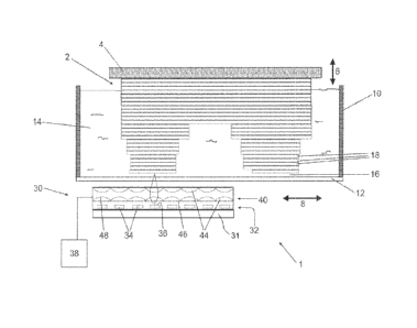
A known illumination system is the one described in W02006/064363
where the light of multiple light sources (LEDs) is collimated by a multi lens
array to provide an essentially uniform illumination on a substrate. The
outgoing beams are slightly diverging, so that the outgoing beams have a
certain overlap on the substrate. A film mask is provided on top of the
substrate for patterning purposes. A similar illumination system is known
from US2009/0002669A1. In contrast to these prior art structures, reference is
first made to Fig. 1, which shows a sectional side view of an exemplary
stereolithography apparatusapparatusl according to an aspect of the
invention. The apparatus 1 may be used for the layerwise production of a
tangible object 2, such as a prototype or model of an article of manufacture.
The apparatus 1 may comprise a carrier plate 4, a liquid reservoir 10, and an
illumination system 30.
During production, the tangible object 2 is suspended from the carrier
plate 4 to which the first-constructed layer of the object 2, and indirectly
also
any subsequent layers, adhere. The carrier plate 4 is moveable in a direction
6
CA 02754337 2011-09-02
WO 2010/101466
PCT/NL2010/050116
4
by means of a drive mechanism (not shown), and is moved upward one layer
thickness each time a new layer has been constructed.
The liquid reservoir 10 may be filled with a liquid, photo-curable resin
14. A bottom plate 12 of the liquid reservoir 10 is optically transparent to
the
light emitted by the illumination system 30, which is to be described
hereafter.
The bottom plate 12 also functions as a construction shape that bounds one
side of a liquid layer 16 to be (partially) solidified. It will be clear that
once a
layer has been constructed, and the carrier plate 4 is moved upward one layer
thickness, the space between the lastly constructed layer and the bottom plate
12 is filled with resin 14, so as to form said liquid layer 16.
The apparatus 1 also comprises an illumination system 30 that is
adapted to selectively illuminate a predetermined area of the liquid layer 16.
As a result of the illumination, a solid layer 18 of the tangible object 2 may
be
obtained, said layer 18 having a predetermined shape in accordance with the
applied illumination pattern. The illumination system 30 includes an LED
array 32 provided on a support 31 and an imaging system that comprises a
multi-lens projector 40. In other embodiments, the imaging system may
comprise a different number of multi-lens arrays, for example just one, and/or
other elements, depending on the desired configuration. In a preferred
embodiment, the number of lenslets in a multi-lens array is approximately
10.000 to 25.000 or more.
The LED array 32 comprises a plurality of LEDs 34. The LEDs 34 are
arranged in a two dimensional plane, preferably in a grid-like fashion, such
that the LEDs compose equidistant and perpendicularly oriented rows and
columns with each LED defining a gridpoint. Each of the LEDs 34 possesses a
light-emitting surface 36 that faces the bottom plate 12 of the liquid
reservoir
10, which is substantially parallel to the two-dimensional plane of the LED
array 32. A controller 38 may be provided to control, i.e. switch off and on
(with desired intensity), individual LEDs 34 in the array 32 so as to create a
CA 02754337 2016-08-26
20184-499
time-varying two-dimensional pattern of lighted LEDs that may be projected
onto the liquid
resin layer 16.
The substantially planar multi-lens projector 40 is disposed in between the
light-
emitting surfaces 36 of the LEDs 34 and the liquid layer 16 to be selectively
cured. The
5 projector 40 comprises a plurality of lenses or lenslets 44, preferably
one for each LED 34.
The lenses 44 may preferably be arranged in correspondence with the
arrangement of the
LEDs 34 in the array 32. The multi-lens projector 40 may be of a piano-convex
type, thus
having one plano side 46 that defines the piano side of all lenses 44, and a
plurality of convex,
partially spheroidally shaped sections 48, one for each lens 44. The lenslets
44 may be
oppositely oriented, as shown in Fig. 1. Together, the multi-lens projector 40
forms an
imaging system that is adapted to image a pattern of lighted LEDs onto the
liquid layer 16 in
such a way, that each lighted LED 34 produces a separate, conjugate spot on a
predetermined
area of the liquid layer 16. The multi-lens projector 40 may be made of a
variety of materials,
including glass and plastic.
The illumination system 30 may be moveably disposed below the bottom plate 12
of
the liquid reservoir 10, such that it can move in a direction 8 parallel to
the bottom plate 12 of
the liquid reservoir 10. The motion of the illumination system 30 may be
controlled by the
aforementioned controller 38, which also may control the lighting of the LEDs
34. In an
embodiment, separate controllers control the motion of illumination system and
the lighting of
the LEDs. In use, the illumination system 30 may be moved rectilinearly in a
direction that
extends at an angle with the perpendicular directions of the rows and columns
of the LED
array 32 to enhance the effective resolution of the system. This technique is
described in more
detail in copending application EP 2 075 110 in the name of applicant.
Accordingly, in
Figure 1, an illumination system (30) for use in a stereolithography apparatus
(1) is shown,
comprising: a planar support 31 supporting a two-dimensional array of
CA 02754337 2011-09-02
WO 2010/101466
PCT/NL2010/050116
6
individually controllable wide-angle light-emitting diodes (LEDs) (34)
comprising light emitting surfaces; and a multilens projector array (40)
arranged relative to the array, and adapted to project the light-emitting
surfaces of the LEDs onto a work area (16). The light emitting surfaces may be
defined by a LED- substrate surface or, equivalently, a planar mask placed
adjacent to the LED-substrate, so that a focussed image of the LEDS is
provided onto the work area (16).
A typical width dimension of the Led array and multilens array is
approximately 50 x 5 cm, to be able to project a scan image on a work area of
approximately 500 x 500 mm. However, the invention is not limited to such
dimensions. Other typical numbers are a projector pixel number of
approximately 10.000 to 25.000 or more, pixels placed in a grid distance of
approximately 2 mm and slightly placed under an angle to form a resolution of
approximately 20 micrometer. (curing layer thicknesses of typically
approximately 50 micrometer). Attainable production speeds of tangible
objects 2 could be typically approximately 20 millimeters per hour or more.
The light is typically UV light in an approximately 300 nm area, in
particular, in a 300-400 nm range.
In the exemplary embodiment shown in Fig. 2, an optical mask 50 is
provided in between the two multi-lens arrays 41, 42. The mask 50 essentially
functions as an aperture stop that blocks light coming from angles of the
light-
emitting surface 36 of an LED 34 that are larger than the numerical aperture
angle. Although in the Figure 2 and Figure 3 embodiments the optical mask 50
is structured as a separate plate-like object alternatively, the optical mask
50
may be provided by for example printing or vapour deposition.
Although the optical mask may be disposed at different positions in the
illumination system, as will be elucidated below, the optical mask is
preferably
disposed in a Fourier plane. At such a position the mask may prevent any
undesired light from entering the imaging system, in which it might disperse,
making it harder to eliminate at a later stage. For a given optical mask and
CA 02754337 2011-09-02
WO 2010/101466
PCT/NL2010/050116
7
LED array, a suitable position between the light-emitting surfaces of the LEDs
and the image plane should therefore allow the mask to serve as an aperture
stop, or in fact a plurality of aperture stops, one for each light-emitting
surface.
Particularly advantageous is the application of an optical mask to a light-
receiving face, in particular a piano face, of a multi-lens array that is part
of
the imaging system. The optical mask may for example take the form of a film
or a coating. A piano side allows the optical mask to be applied easily,
whereas
application to the multi-lens array does away with the necessity to align a
separate optical mask relative to the multi-lens array during assembly of the
illumination system. The above-mentioned and other features and advantages
of the invention will be more fully understood from the following detailed
description of certain embodiments of the invention, taken together with the
accompanying drawings that are meant to illustrate and not to limit the
invention.
In Figure 3 and Figure 4, embodiments are shown of an illumination
system 30 wherein the lenslets (44) are arranged in direct abutment on a
lenslet convex side with another optical element (43) in the stack. In
particular, multilens projector array (40) is formed by a stack of optical
elements 41, 42, 43, 45, including a plurality of lenslets 44 in the form of a
lenslet body 41, 42, in direct abutment on a lenslet convex side with another
optical element 42, 43 in the stack.
Accordingly an illumination system 30 is provided for use in a
stereolithography apparatus 1, comprising a planar support supporting a two-
dimensional array 32 of individually controllable wide-angle light-emitting
diodes (LEDs) 34; and a multilens projector array 40 arranged relative to the
array, and adapted to project the LEDs onto a work area 16; wherein the
multilens projector array 40 comprises a stack of optical elements including a
plurality of lenslets in direct abutment on a lenslet convex side with at
least
another optical element in the stack.
CA 02754337 2011-09-02
WO 2010/101466
PCT/NL2010/050116
8
In particular, in these embodiments the multilens projector array (40)
comprises lenslet bodies 41, 42 each formed as a plano-convex multilens array;
wherein at least one convex side of a lenslet body 41 or 42 is in direct
abutment on contact zones 44 arranged over substantially the entire body
surface with another element of the stack (piano 43 in Figure 3).
In Figure 4 this other optical element is formed by lenslet body 42
arranged with opposed convex sides in direct abutment; the projector 40 thus
forming an essentially rigid body supported by the planar support 31. In
Figure 3 spacers may be provided as protruding ridges 400 cast integral in
support 31, and in direct contact with the piano side 46 of the lenslet body
41.
A difference between the two embodiments is the presence (Figure 3)
or absence (Figure 4) of a piano body 43 between the two multilens arrays 41,
42. Both embodiments have the advantage that a rigid structure is provided
that is easy to implement, and has high structural tolerance. In particular,
the
support 31 is a rigid support, for example, of an aluminium plate and
comprises, for example further cooling structures such as coolant channels or
heat fins to form a heat sink for the LEDS. By this structural assembly,
forces
exerted to the planar surface, for example, by a resin applying device 60
applying resin layer 16, can be led through to a rigid support 31.
Such a resin applying device 60 may be a resin foil guide, which may
be arranged to provide a resin foil in moving contact with the work area 16,
which typically exerts a pressure onto the projector body 40 and which is
addressed in order to enhance properly patterned illumination by the LED
arrays 32. Pressing forces onto the projector 40 may be provided by a variety
of
other sources, including acceleration forces etc. An exemplary embodiment of
such device 60 is disclosed by the stereolithographic apparatus of Figure 7.
Although in principle, optical arrangements demand strict dimensional
tolerances; due to the nature of stereolithographic curing, the imaged pixel
area in the curing layer may not be identical to the imaged LED light emitting
surface 36; which relaxes the constraint of in-focus imaging. In particular,
in
CA 02754337 2011-09-02
WO 2010/101466
PCT/NL2010/050116
9
an embodiment, the stacked lenslet bodies 41, 42 are formed with opposed
convex sides in direct abutment on contact zones arranged over substantially
the entire body surface; so as to form a flat rigid projector body 40. Here,
remarkably, a slight flattening tolerance is allowed of the convex lenslets 44
that are in direct abutment, since near the optical axis, the image of the
LEDS
can be projected without optical power. This confirms the inventive principle,
that the pixel area in the curing layer may not be identical to the imaged LED
light emitting surface 36; which relaxes the constraint of in focus imaging.
The
flattening, due to shortening of the lenslet along the optical axis may be
roughly one half of the LED light emitting surface diameter. This flattening
may be predesigned to increase the geometrical stability of the projector body
40 and to ease the assembly of the lenslet bodies 41. In addition, the
lenslets
may be of a Fresnel type, wherein annular lens portions may be provided. The
inner lens portion may be flat or at least flattened. Such lenslet
arrangements
may be used to further decrease a height dimension and/or stabilize the lens
projector body 40.
Figure 3 and Figure 4 accordingly illustrate that the projector stack 40
is in direct abutment on contact zones 400 arranged over substantially the
entire surface with the projector support 31 of illumination system 30. Here,
abutment over contact zones 400 arranged over substantially the entire
surface is meant to encompass configurations with isolated supports, such as
depicted in the Figure 3 and Figure 4, as long as the sagging of the support
is
minimal in view of a pressing force exerted on the projector stack surface
451.
In an embodiment, typically a support point 400 may be provided per
light channel, or one support point for every 2 x 2 light channels, or for
every 5
x 5, 10 x 10 etc. light channels. In addition, the entire element surface may
be
supported, for instance protective plate 45 is supported over its full area by
lenslet body 42.
Accordingly, preferably each constituting element of illumination
system 30A, 30B is supported by one of the lower elements in the stack,
CA 02754337 2011-09-02
WO 2010/101466
PCT/NL2010/050116
typically by a support structure immediately beneath the layer itself in
direct
abutment on at least one ¨ for a structure supporting the entire surface, such
as, in an embodiment, a transparent layer such as piano 46 or resin layer 33,
see herebelow, or on many contact zones arranged over substantially the entire
5 element surface.
The supports may be formed by bare LED dies 34. This may have an
additional advantage of accurate Z-alignment of the dies by forming a flat
levelling contact with the piano side 46 of the projector stack 40.
In all, preferably the disclosed embodiments are formed by a rigid
10 stack defining compact and rigid illumination systems, such as those
disclosed
in 30A-F. The system 30 includes (from bottom to top) an electronics board 311
(printed circuit board, possibly flexible), optionally itself comprised of a
number of layers of different materials and the projector 40 formed by a stack
of optical elements. The mechanical link between the carrier 31 and the next
higher layer may be e.g. a set of ribs 400 protruding upward from the carrier
31. Alternatively individual blocks (each having a flat top and bottom), or a
plate with holes to leave space for the light sources (LEDs) may be provided
(not shown).
The projector body 40 then is formed by a lower lens array 41, typically
comprised of a piano side formed by a transparent, e.g. glass plate 46. a
layer
412 of lenslets 44, for example of a transparent plastic, and typically having
a
flat bottom side in contact with the glass plate 46 and on the top side a
multitude of convex lens surfaces 44.
In addition a support plate 45, e.g. of glass material and a protection
film (not shown) can be provided typically defining a very short, almost zero
working distance on working area 16. It is noted that this can be conveniently
combined with the large NA working principle according to the invention
demanding short, preferably (almost) zero working distances.
An advantage of the piano body 43 in Figure 3 is that the X-Y
alignment of the convex shaped lenslets bodies 41 42 is easier to control. In
CA 02754337 2011-09-02
WO 2010/101466
PCT/NL2010/050116
11
addition, a transparent top piano 45 may be attached to the multilens arrays
to facilitate replacement of a work surface. While Figure 3 shows spacers 400
as integrated elements of the support, a separate platelike structure could be
provided as in Figure 4. This structure could also serve as an aperture
defining
mask structure according to the inventive principle.
In another embodiment, illustrated in Figure 5 alternatively, a resin
layer 33 forming a reinforcement layer between the carrier 31 including the
LED array 32, may be provided. The resin 33 may improve the structural
stability of the support since sagging of the piano 46 between supports 400
(as
depicted in Figure 3) can be prevented. At the same time optical transmission
between the LEDs 34 and the projector 40 can be enhanced. Furthermore, a
sealing edge around the projector body may be reduced in size or altogether
omitted, reducing the projector mass and size. Typically, the resin has a
refractive index of around 1.3 or larger, for example, 1.5 and can be photo-
curable silicone resin. While the resin may be of a curable type, additionally
or
alternatively, an optical transmission fluid may be provided, even in other
parts of the stack, for example between lenslet arrays 41, 42, to improve the
optical transmission and further improve the structural stability of the
stack.
This can for example be done by stacking, sealing and filling the stack with
optical transmission fluid of a desired refractive index, and possibly curing
the
fluid. The LED material is typically a AlGaN having a refractive index of
around 2.5. To optimize the transmission the resin does not have to be a
continuous layer but may be applied in blobs, as long as each LED is covered,
and the space between the LED and the optical part above it is filled.
Suitable
resin materials are transparent for the radiation used, which in an
embodiment may be UV radiation around 365 nm. The material preferably has
a refractive index higher than 1.3 which provides optical design latitude, in
practice a value between the refractive index of the LED material and the
refractive index of the piano 46. In a practical embodiment, a resin
commercially obtainable under the trade name Sylgard 184 with refractive
CA 02754337 2011-09-02
WO 2010/101466
PCT/NL2010/050116
12
index n = about 1.55 was used. Other material choices may be for example
acrylate, polycarbonate.
Without said optical immersion by the resin layer 33, transmission
losses between the LED outcoupling and the projector incoupling may involve
about 22%, where the addition of the resin layer may improve the transmission
to a loss of only about 7%. Accordingly, an optical power transmission
improvement of about 20% can be provided. Conveniently, the resin is of a
photo-curable type, which can be cured by use of LEDS 34. In an embodiment,
additionally, rigid spacers (not shown) are provided in the curable resin to
improve the structural stability. The spacers may be removed after curing.
Alternatively, the spacers are formed by the LED surfaces where only a thin
film of resin may form a power transmission interface. Conveniently, the resin
protects the mechanical integrity of the LED-bondings, in particular, the
electrical circuit bonds.
In another embodiment 30E, illustrated in Figure 6A, supports can be
embodied as protrusions 440 moulded on concave sides between the convex
optical surfaces 44 of lens layer 42 or as an intermediate supporting layer
501
in illumination system 30F (Figure 6 B). Alternatively the supporting layer
may be formed by a number of isolated supports, e.g. balls, but preferably,
the
layer is formed by an integral perforated plate 501 formed with perforations
for the optical paths. Conveniently, anti-straylight mask 50 of Figure 2 can
be
used for such purpose.
The orientation of the illumination device 30 may well be inversed to
have the LEDs arranged on a top piano surface and a working area arranged
on a bottom side.
Alternatively as shown in Figure 6B the array 32 of light-emitting
diodes (LEDs) 34 may be arranged with bare dies aligned in contact with the
piano side 46 while having electrical contact from a circuit board (not shown)
arranged on the support 31.
CA 02754337 2011-09-02
WO 2010/101466
PCT/NL2010/050116
13
Additionally, preferably the multilens projector array is arranged to
project light from angles larger than a focused numerical aperture angle in a
conventional optical design. Here, the focused numerical aperture angle is
defined as the maximum entry angle of the outermost ray into the projection
optical system that can be imaged in focus. More specifically, said multilens
projector array is arranged to project light from the LED array emitted from
angles larger than a maximum entry angle of an outermost ray entering the
projector array that can be imaged in focus. Here the entry angle is measured
relative to an optical axis or normal direction of the projector array. Thus,
the
"focused numerical aperture" value (FNA), is defined as n*sin(thetaf) where
thetaf is the angle of the outermost ray that is well focused by the system.
One
further definition of focus may be that a ray is imaged within approximately 5
um, preferably within approximately 2 um from the image of a central ray.
Normally, in a design of an optical system the maximum entry angle is chosen
to be not larger than the focused numerical aperture. A well-known
characterization of a numerical aperture is NA = n sin 0 wherein 0 defines a
maximum entry angle of light into the projector system (irrespective of it's
focussing behaviour); and n is the refractive index of the projector. A
typical
numerical aperture value of a projector system is 0,2. In one
characterization,
the numerical aperture of the projector system according to an aspect of the
invention is at least approximately 0,3 ¨ to values ranging to 0, 8 or even
above 0,8.
The solution offered by the present invention is based on the
understanding that depending on the lens design, one can distinguish a FNA
value for points in the central area of the emitting surface and for points in
the
edge area of the emitting surface. The inventors found, that for the effective
total spot quality the FNA of the edge area points is most important, and that
the optical design of the lens system can be made or changed to provide large
FNA for edge area points while allowing the FNA for central area points to be
reduced.
CA 02754337 2016-08-26
20184-499
14
Accordingly, the multilens projector array preferably utilizes a larger
numerical
aperture than would be conventionally feasible, in particular, with a lens
arrangement of no
more than two lens stacks, by relaxing the focusing quality of the projector
array in a specific
way. This is preferably obtained by designing the optical surfaces such, that
the image quality
is only corrected at the outer edges of the LED image in the resin. According
to one
characterization, the focusing quality of the outer edge parts of the LED
image is at least equal
or even better than the focusing quality of the central parts. As an example,
in a typical
projector setup, a central point of the LED may be imaged in a region of about
30 micron
diameter, for example, in a region extending between about 25 and 40 micron;
wherein a
peripheral point of the LED may be imaged in a region of about 20 micron
diameter, for
example, in a region extending between 10 and 25 micron; illustrating a
focusing quality of
the edges which is about a factor 1.5 better than the focussing quality in the
central parts.
Typically, the focusing quality of the edge areas is at least equal to the
focusing quality of the
central area.
Furthermore, the image quality criterion used may be more relaxed than
conventionally expected, because advantage is taken from the thresholding
behaviour of the
resin.
Figure 7 shows a further embodiment of a resin applying device 60 arranged to
provide a resin foil in moving contact with the work area 16, which typically
exerts a pressure
onto the projector body 40 and which is addressed in order to enhance properly
patterned
illumination by the LED arrays 32.
The system 120 is disclosed in application WO 2010/074566 and comprises a
construction shape in the form of a flexible foil 106. On the foil 106, a
liquid layer 100 is
formed of limited height to be brought in contact with the tangible object
150. The presently
disclosed illuminator embodiments 30 are arranged, by suitable control of the
LED array, to
solidifying a predetermined area of a layer of the liquid 100, said liquid
layer 100 adjoining
the foil 106, so as to obtain a solid layer of the tangible object 150, the
solid layer thus having
a predetermined shape.
CA 02754337 2016-08-26
20184-499
To enable the light or other radiation of the illuminator 30 to solidify the
liquid layer
100, the flexible foil 106 is preferably substantially transparent to the
radiation at least having
film 106 clear on only one side and optionally matte or clear on another side.
In the embodiment a movable foil guiding stage 180 is located below the
construction
5 shape 15. Further, in the shown example embodiment, the illuminator 30 is
positioned on the
movable foil guiding stage 180, between foil guiding elements 60, to expose
the layer of
uncured material through the foil 106.
In the embodiment, each time after solidification and separation of a new
layer, carrier
plate (z-stage) 15 together with the tangible object 150 including solidified
layers adhered
10 thereon are moved upwards. Hence, the method for layerwise production of
a tangible object
is a cyclic method, wherein the described steps of positioning, solidifying,
and separating
together are comprised in a single cycle step of the method.
In the shown example, the foil 106 is transparent to radiation from
illuminator 30.
Movable z-stage 140 can be moved in a z-direction before a new layer of
curable material is
15 provided to the tangible object 150.
The foil 106 can be arranged for carrying the curable layer material 100
supplied from
a dispenser (not shown) to the tangible object 150 and for carrying the
removed uncured
material away from the tangible object 150.
In one embodiment, for each layer two process steps are always required
providing a
layer of resin on foil 106, exposure of the resin; in many applications there
is also releasing
the unexposed resin from the building surface ('peeling' in the example of the
drawing).
The system 120 can be provided with vibration damping 200 and a protective
cap.
A controller can be arranged to control the method steps carried out by the
system 120.
CA 02754337 2016-08-26
20184-499
16
Although illustrative embodiments of the present invention have been described
with
reference to the accompanying drawings, it is to be understood that the
invention is not
limited to these embodiments. While certain embodiments detail certain
optional features as
further aspects of the invention, the description is meant to encompass and
specifically
disclose all combinations of these features unless specifically indicated
otherwise or
physically impossible. Various changes or modifications may be effected by one
skilled in the
art without departing from the scope of the invention as defined in the
claims.