Note: Descriptions are shown in the official language in which they were submitted.
CA 02758803 2011-10-13
WO 2010/119113 PCT/EP2010/054994
1
LOW POWER ACTIVE MATRIX DISPLAY
FIELD
The disclosure relates to low power active matrix displays.
BACKGROUND INFORMATION
Low power displays are essential system components of most mobile
electronic devices. The display subsystem is often one of the largest
consumers of battery power as well as one of the most expensive
components in many of these devices. The display industry has made
continuous progress improving the visual performance, power consumption
and cost through device and system architecture innovations. However,
there is a class of important applications that require additional significant
improvements in power and cost to become technically and financially viable.
The dominant display technology for mobile devices, computer
monitors and flat panel TVs is currently amorphous silicon hydrogenated thin
film transistor (a-Si:H TFT) liquid crystal, also known generally as active
matrix LCD technology. Advanced manufacturing technologies support a
highly efficient worldwide production engine with capacity of over 100 million
square meters of flat panel displays per year. The most common display
architecture in this technology consists of a simple array of TFT pixels on a
glass panel that are driven by one or more driver ICs.
One significant barrier to building displays in a-Si:H TFT processes is
the poor performance and long term reliability of the a-Si:H TFT devices.
Compared to single-grain silicon CMOS technology a-Si TFTs have very low
electrical mobility which limits the speed and drive capability of the
transistors
on the glass. Additionally, the a-Si TFT transistors can accumulate large
threshold voltage shifts and subthreshold slope degradations over time and
can only meet product lifetime requirements by imposing strict constraints on
the on-off duty cycle and bias voltages of the transistors. "Electrical
Instability of Hydrogenated Amorphous Silicon Thin-Film Transistors for
CA 02758803 2011-10-13
WO 2010/119113 PCT/EP2010/054994
2
Active-Matrix Liquid-Crystal Displays" and "Effect of Temperature and
Illumination on the Instability of a-Si:H Thin-Film Transistors under AC Gate
Bias Stress" give a good overview of the gate bias stress induced threshold
shifts and subthreshold slope degradations seen in a-Si:H TFTs.
The positive and negative stress accumulation processes have very
different accumulation rates and sensitivities to gate drive waveforms. To
first order within the range of driving waveforms used in typical flat panel
refresh circuitry, the accumulation of positive stress is not strongly
dependent
on the frequency content of the gate waveform and accumulates relatively
rapidly as a function of the integrated "on" time and voltage of a given gate.
As positive stress is applied the voltage threshold of the TFT device is
typically increased. TFT circuits typically have a maximum allowable positive
threshold shift beyond which the desired device functionality ceases.
Negative stress accumulation, in contrast, depends strongly on
frequency in the range of frequencies normally used in flat panel displays,
accumulating more slowly at higher frequencies. Negative stress
accumulation typically manifests as both negative threshold shift and
subthreshold slope degradation. For negative stress to have a significant
affect, the gate of a typical a-Si TFT needs an unbroken stretch of negative
bias (e.g. 100ms or more for typical a-Si:H TFT devices). In conventionally
scanned TFT flat panel displays, the gate voltage is positive only for a very
small time (e.g. one line time, about 15us every 16.600ms frame; about 0.1%
duty cycle) and negative for the rest of the frame period (e.g. 16.585ms or
about 99.9% of the frame period). Were it not for the strong frequency
dependence of the negative stress, conventional 60Hz panel drive would
have a very short operational lifetime as negative stress accumulation would
quickly render the display non-functional.
One of the key techniques to minimize system power of electronic
systems is to limit or reduce the operation frequency. Power dissipation is
often nearly proportional to refresh frequency in typical TFT LCD displays. In
some applications where the displayed content does not require a fast optical
CA 02758803 2011-10-13
WO 2010/119113 PCT/EP2010/054994
3
response (e.g. slowly updated or static information) the power dissipation of
a TFT LCD can be reduced significantly by driving the frame refresh at e.g.
1 Hz vs. a conventionally scanned 60Hz. Such a reduction, while favorable for
power, is problematic for the device. First, the optical quality of the
display is
compromised; at low frame rates the display can flicker significantly.
Second, at low frame rates the negative stress accumulation of the pixel
TFTs occurs much more rapidly than at 60Hz and will quickly degrade the
functionality of the display. As a result, while frame rate reduction from
60Hz
to 30Hz or even 20Hz has been used as a power reduction technique, TFT
device reliability limits prevent further frame rate reductions in
conventional
displays. The display described herein addresses these limitations.
There are display applications where battery life of months or years
is desired if not required e.g. electronic books, signs and price labels. A
large
set of new display technologies has been developed to address such
markets that require little or no power between displayed content changes.
Such displays are often referred to as electronic paper or bi-stable displays.
This class of displays is primarily used in a reflective mode to minimize
power. For devices whose primary utility is based on the display of
information (e.g. mobile email, e-books, marketing messages) such utility is
enhanced by display technologies that allow longer active display times
between battery recharges or changes. The display described herein is
directed to such applications.
SUMMARY
A display system that substantially prevents negative stress
accumulation in low frame frequency refreshed TFT displays is disclosed.
A display system that substantially lowers power in low frame
frequency refreshed TFT displays is disclosed.
A display system that minimizes power and prevents negative stress
accumulation through temporal and amplitude modulation of the drive
waveforms is also disclosed.
CA 02758803 2011-10-13
WO 2010/119113 PCT/EP2010/054994
4
A display system that substantially lowers power in low frame
frequency refreshed TFT displays using an external driver IC is disclosed.
Further objects, aspects, and advantages of the present teachings
will be readily understood after reading the following description with
reference to the drawings and the appended claims.
BRIEF DESCRIPTION OF THE DRAWINGS
Figure 1 shows a representative prior art reflective TFT LCD cross
section.
Figure 2 shows a representative circuit diagram for a prior art TFT
LCD array.
Figure 3 shows a representative prior art ESD circuit element and its
associated nonlinear IN transfer curve.
Figure 4 shows a representative set of voltage waveforms for a prior
art frame inversion drive method of the prior art TFT circuit in Figure 2.
Figure 5 shows a representative prior art variation in the frequency
response of positive and negative gate bias stress accumulation of a-Si:H
TFTs.
Figure 6 shows a representative block diagram of a TFT LCD
electrical system with an external row and column driver IC.
Figure 7 shows a representative circuit diagram of the TFT portion of
an LCD.
Figure 8 shows a representative circuit diagram of an alternative
implementation of the TFT portion of an LCD.
Figure 9 shows a representative TFT pixel circuit schematic.
Figure 10 shows a representative TFT pixel circuit layout.
Figure 11 shows a representative first set of voltage waveforms
associated with the operation of the TFT pixel circuit in Figure 9.
Figure 12 shows a representative second set of voltage waveforms
associated with the operation of the TFT pixel circuit in Figure 9.
Figure 13 shows a representative third set of voltage waveforms
CA 02758803 2011-10-13
WO 2010/119113 PCT/EP2010/054994
associated with the operation of the TFT pixel circuit in Figure 9.
Figure 14 shows a representative flow chart indicating the operations
of the TFT LCD.
Figure 15 shows a representative output multiplexer of a row driver
5 circuit for generating the waveforms of Figures 12 and 13.
Figure 16 shows a representative step-wise charging of two internal
signals of a row driver circuit.
Figure 17 shows a representative transfer function for a thin film
transistor (TFT).
Figure 18 shows a representative electronic shelf label with a display.
Figure 19 shows a representative electronic shopping cart handlebar
with a display.
Figure 20 shows a representative electronic book with a display.
Figure 21 shows a representative cell phone with a display.
Figure 22 shows a representative portable music player with a
display.
Figure 23 shows a representative flat panel TV, monitor or digital
signage with a display.
Figure 24 shows a representative notebook computer, digital picture
frame or portable DVD player with a display.
Figure 25 shows a representative digital billboard with one or more
displays.
GLOSSARY OF TERMS
The following abbreviations are utilized in the following description,
which abbreviations are intended to have the meanings provided as follows:
a-Si - amorphous silicon
AC - alternating current
CMOS - complementary MOS (both P and N type FETs available)
COM - common electrode in an LCD device
DC - direct current
CA 02758803 2011-10-13
WO 2010/119113 PCT/EP2010/054994
6
ECB - electrically controlled birefringence
ESD - electro static discharge
ESL - electronic shelf label
FET - field effect transistor
IC - integrated circuit
IDS - drain to source current
LCD - liquid crystal display
MOS - metal oxide semiconductor
MTN - mixed-mode twisted nematic
NMOS - N-channel MOS
OCB - optically compensated bend
PDLC - polymer dispersed liquid crystal
RGB - red, green, blue
RGBW - red, green, blue, white
RMS - root mean square
RTN - reflective twisted nematic
TFT - thin film transistor
VGS - gate-source voltage
DETAILED DESCRIPTION
Each of the additional features and teachings disclosed below may
be utilized separately or in conjunction with other features and teachings to
provide improved low power displays and methods for designing and using
the same. Representative examples, which examples utilize many of these
additional features and teachings both separately and in combination, will
now be described in further detail with reference to the attached drawings.
This detailed description is merely intended to teach a person of skill in the
art
further details for practicing preferred aspects of the present teachings and
is
not intended to limit the scope of the claims. Therefore, combinations of
features and steps disclosed in the following detail description may not be
necessary to practice the concepts described herein in the broadest sense,
CA 02758803 2011-10-13
WO 2010/119113 PCT/EP2010/054994
7
and are instead taught merely to particularly describe representative
examples of the present teachings.
In addition, it is expressly noted that all features disclosed in the
description are intended to be disclosed separately and independently from
each other for the purpose of original disclosure, as well as for the purpose
of
restricting the subject matter independent of the compositions of the features
in the embodiments and/or the claims. It is also expressly noted that all
value
ranges or indications of groups of entities disclose every possible
intermediate value or intermediate entity for the purpose of original
disclosure,
as well as for the purpose of restricting the claimed subject matter.
Figure 1 shows a simplified cross section of a reflective single
polarizer TFT LCD flat panel display 100. The control circuitry 102 is
fabricated on a substrate 101. Control circuitry 102 may be implemented
preferably in an amorphous-Si process but can alliteratively be implemented
with any thin-film switch-capable backplane technology, i.e. any inorganic or
organic semiconductor technology. Substrate 101 can be glass, plastic,
quartz, metal, or any other substrate capable of supporting switching device
fabrication. Electrode 103 can be formed by photolithographic, embossing,
printing and/or chemical processes and can be textured to diffusely reflect
incident light. Liquid crystal display material 104 sits in between the top
and
bottom plates. Color filters 106 and a top plate transparent conductor 105
driven by a voltage conventionally labeled "COM" (for "common") are
deposited on the top substrate 107. A retardation film or quarter wave plate
108 can be placed on top of the upper substrate 107. A diffusing polarizer
109 completes the LCD stack 100. In typical operation incident light 110 is
polarized, filtered and diffusely reflected by the LCD stack 100 to create a
reflected image 111.
Alternative display materials and constructions other than that shown
in Figure 1, such as those with a flat reflector layer, a dual polarizer
reflective
with a reflector outside the lower glass substrate, transmissive,
transflective,
backlit, sidelit, frontlit, guest host LCD, electrically controlled
birefringent,
CA 02758803 2011-10-13
WO 2010/119113 PCT/EP2010/054994
8
RTN, MTN, ECB, OCB, PDLC, electrophoretic, liquid powder, MEMs,
electrochromic, or other alternate electrically controlled display
technologies
that require an active backplane can benefit from the present teachings. The
specific description herein of a reflective LCD incorporating the present
teachings does not limit the scope of the present teachings in their
application to alternative display materials and technologies.
Figure 2 shows a typical circuit diagram of a conventionally scanned
prior art TFT display. At each intersection of a row gate line R0 to RM_1 200
and a column source line CO to CN_1 201 is a TFT pixel 202 which consists of a
single TFT transistor 203, a storage capacitor CST 204 and a liquid crystal
capacitor CLc 205 formed between the reflective electrode Pm,n 103 206 and the
common (COM) counter glass electrode 107 207. Row lines Rm 200 are
typically driven to sequentially pulse "on" each row of TFT transistors which
captures the voltages driven on the column lines Cn 201 into the array of
pixel
storage CST 204 and LCD capacitors CLc 205 to form an array of pixel voltages
Pm,n 206 and a corresponding image.
In Figures 1 and 2, each electrical connection to the TFT substrate
101 is protected against electrostatic discharges with an ESD protection
device. The column line ESD devices 208 are attached to a first floating bar,
FB1 209, and the row line ESD devices 210 are attached to a second floating
bar, FB2 211. The two floating bars FB1 209 and FB2 211 are subsequently
connected to the COM electrode 207 with two additional ESD devices, 212
and 213 respectively. Those skilled in the art will recognize that the ESD
protection scheme shown in Figure 2 is one of many possible ESD
protection schemes in common use. For very low power displays, ESD
circuits are typically a major consumer of static power in the active devices
on
the display substrate 101.
Figure 3 shows a typical four TFT ESD protection device commonly
used in flat panel displays. It consists of four diode connected transistors
300 301 302 303, half of which will be forward biased when the voltage
across the two terminals A 304 and B 305 is highly positive or negative. For
CA 02758803 2011-10-13
WO 2010/119113 PCT/EP2010/054994
9
low voltage operation the current is close to zero as shown in the associated
IN curve 306. To minimize leakage power in ESD devices, typically the
voltage waveforms applied to the TFT substrate 101 should be kept at a
voltage as close to that of COM 207 as possible while maintaining the desired
operation. Those skilled in the art recognize the wide variety of TFT ESD
protection sub circuits available; for the purposes of the present teachings
any device or combination of devices that have nonlinearly increasing current
as a function of applied absolute voltage can be substituted without
limitation.
Liquid crystals are commonly driven with AC pixel voltage signals
that invert polarity at the display's frame rate. Such bipolar drive is
commonly
necessary to prevent damage to the liquid crystal that can occur if
significant
DC voltages (e.g. a few volts or more) are applied for a significant period of
time (e.g. tens of seconds or more). Such damage often accumulates over
the life of the panel and can lead to image burn-in, image sticking, loss of
contrast or other visible defects. Typical LCD materials are designed to
respond approximately to the RMS of the AC signal over a wide range of
frequencies.
To achieve AC pixel drive several techniques are commonly used.
The simplest and lowest power is frame inversion wherein all of the pixels in
the frame are first written with a positive polarity frame followed by an
entirely
negative polarity frame. Often the COM counter electrode that forms the back
plate of the storage capacitor CST and the LC capacitor CLC is modulated from
the positive frame to the negative frame to reduce the voltage range of the
column source driver IC, saving power and cost. Despite the simplicity and
power/cost advantages, frame modulation can lead to noticeable flicker if the
two frames (positive and negative) are not balanced well.
To mitigate the flicker effect from unbalanced frame inversion, the
COM counter electrode can be modulated on a per line (or multiline) basis
during the frame scanning process.
This maintains the low voltage range of the column source drivers
while incurring higher power to drive COM as the COM electrode is highly
CA 02758803 2011-10-13
WO 2010/119113 PCT/EP2010/054994
capacitive. For a given amount of imbalance between positive and negative
pixel drive the line inversion technique generates less visible flicker as the
two polarities are typically tightly interleaved spatially (e.g. even and odd
lines
are alternating polarity). An additional level of positive and negative pixel
5 interleaving (both horizontally and vertically on the display) called dot-
inversion is generally regarded as the best visually for a given imbalance but
also has the highest power consumption and requires higher voltage range
column driver ICs compared to the line or frame inversion techniques.
Drive waveforms for displays can be described and synthesized in
10 many forms; in what follows, for simplicity and clarity, a simple multi-
level
drive waveform description is generally used that facilitates the exposition
of
the present teachings. Signal names beginning with the letter "V" are
generally used herein to indicate a DC voltage level that can be used for
multi-level waveform synthesis (e.g. by using a switch or mux). Those skilled
in the art will recognize the wide variety of waveform description and
synthesis methods (e.g. analog waveforms, buffer amplifiers, etc.); the
present teachings are applicable to the many available waveform
descriptions, synthesis methods and hardware implementations thereof.
Figure 4 shows a typical set of drive waveforms for the conventionally
scanned prior art TFT display of Figure 2 using the COM modulation
technique for frame inversion. Depending on the desired polarity of the
frame, the COM node 401 is driven to one of two DC levels VCH 402 or VCL
403. For a TFT technology with a threshold voltage near zero, a selected row
line must be driven well above the desired pixel voltages Pm,n 206 to create
conduction in the pixel TFT 203. Column source lines C[N-1:0] 404 (notation
for the set of lines CO to CN_1) are driven with the desired pixel voltages
for a
given row of pixels while the corresponding row gate voltage is pulsed to a
high gate voltage VGH 405. For the present example, a bi-level column drive
waveform using two DC data voltages, VDH 406 and VDL 407 will be used to
simplify the description and drawings. As is well known in the art the column
lines can be driven with analog voltages between VDH 406 and VDL 407 to
CA 02758803 2011-10-13
WO 2010/119113 PCT/EP2010/054994
11
create a grayscale response in the LCD material 104. The present teachings
can be generally applied to binary, multilevel and/or continuous analog
column line drive.
Column source lines C[N-1:0] 404 thus set the voltage on the desired
row of pixel storage capacitors 204. Subsequent rows of pixels are refreshed
by sequentially driving all of the row gate electrodes high to VGH 405 then
low to VGL 408 (e.g. RO 409 and R1 410 in Figure 4) until the complete array
of pixels is written. For frame inversion TFT LCDs, the aforementioned DC
voltage levels obey the following relationship: VGH > VCH > VDH > VDL >
VCL > VGL. Note that VGL typically needs to be negative enough to keep
pixel TFT 203 in the "off' state despite the negative shift in the pixel
voltage
(Pn,m, especially for black, e.g. point 411 of Figure 4) when the COM 401
node transitions low to level VCL 403.
Non-zero gate bias of N-type a-Si:H TFT devices is typically required
to both activate and deactivate the devices. Positive gate bias in such
devices turns the device "on" and typically induces a positive shift in the
threshold voltage of the device over long time scales.
Negative gate bias turns the device "off" and typically induces both a
negative threshold shift and subthreshold slope reduction over long time
scales.
Stress accumulation in a-Si:H TFTs is generally thought to follow a
stretched exponential of the form:
AV, (tsT) = OVT (tsT) + AV,- (tsT )
where the positive stress component:
AVT (tsT) = A+VV+ (tsT * D) P+
and the negative stress component:
AVT (tsT) = A - V V (tsT * (1- D)) I FTw
act relatively independently; where AVT is the threshold shift, VG is the
gate bias less the threshold voltage of the device, tST is the total stress
time, A
is an empirical constant, D is the duty cycle of the positive part of the
drive
CA 02758803 2011-10-13
WO 2010/119113 PCT/EP2010/054994
12
signal and Fpw is a factor between zero and one indicating the negative stress
accumulation frequency dependence. Generally the stress induced threshold
shift is proportional to the gate drive amplitude (VGS-VT) raised to a power
around 1.5 to 2.0 and approximately the square root of the total stress time
accounting for duty cycle (e.g. a+/- - = 1.7 and R+/- - = 0.4). Due to the
approximately square law dependence on voltage, a short duration high
amplitude gate drive signal can generate significantly more stress than a
lower gate voltage applied over a longer period of time; in a preferred
embodiment, the gate drive amplitudes are minimized and charging time and
TFT size are maximized to lower the required VGS gate drive and minimize
TFT stress.
Figure 5 shows a representative relationship between the drive
waveform frequency 501 and the accumulation of positive and negative AC
stress relative to the accumulation of DC stress 500 (effectively the Fpw
factor for negative stress) typical of a-Si:H TFTs. Typically the positive
stress
502 is independent of a wide range of typical gate signal frequencies
whereas the negative stress 503 is highly dependent on frequencies of
interest to low power refresh operation. For conventionally scanned TFT
LCD displays, the frame rate is relatively high (e.g. 60Hz) compared to the
characteristic cutoff frequency in negative stress; as a result the negative
stress is substantially reduced relative to its DC value. This reduction is in
fact absolutely necessary since the negative stress has nearly 100% duty
cycle in a conventional driving scheme and without negative gate bias AC
modulation such displays would fail rapidly (days or weeks).
Negative and positive stress accumulation mechanisms are theorized
to be affected very strongly by the density of charges (holes and/or
electrons)
in the TFT channel. When a gate is biased with a positive VGS, electrons are
available immediately from the source and/or drain and very rapidly fill the
channel. Due to the rapid charging of the channel, the positive stress
exhibits very little frequency rolloff in the range of interest for displays
(below
100kHz).
CA 02758803 2011-10-13
WO 2010/119113 PCT/EP2010/054994
13
Negative bias, however, depletes the channel of electrons and forms
a potential well for holes. Holes, however, due to their limited mobility and
the lack of a source in an NMOS device, accumulate much more slowly than
electrons in the TFT channel. The slow rate of hole generation and
accumulation in the channel is the basis for the rapid dropoff in accumulated
stress as the frequency of the gate modulation is increased. By periodically
pulsing the gate voltage to a positive level, holes that have accumulated are
either injected into the source or drain or recombine with incoming electrons.
In either case, a short, slightly positive VGS clears the holes from the
channel
and neutralizes the negative stress mechanism.
Fiat panel display power can be broken down into two main
categories: dynamic power which is more or less proportional to the frame
frequency and static power which is relatively independent of frame
frequency.
In order to reduce the dynamic power dissipation of a flat panel
display, the frame rate is desirably reduced. However for conventionally
scanned displays lower frame frequency results in lower negative stress
frequency which increases the effect of the negative stress to the point where
the lifetime of the flat panel can be substantially shortened. The present
teachings describe a circuit technique that mitigates such negative stress at
very low frame rates (e.g. 1 Hz) to achieve very low power refreshed
displays. In addition, the present teachings detail a technique wherein the
dynamic power dissipation can be concentrated on a few line drivers of a
driver IC so that charge sharing or adiabatic charging methods can be used
to further reduce power.
ESD circuits of a conventionally scanned display often consume
negligible power compared to the driver ICs and backlight. However for
reflective flat panel displays driven at very low frame rates (e.g. 1 Hz) the
power consumed by the ESD protection devices can become a significant
fraction of the total power consumption. In order to reduce the static power
dissipation of a low frame rate flat panel display, the ESD circuit power
CA 02758803 2011-10-13
WO 2010/119113 PCT/EP2010/054994
14
dissipation is desirably reduced. A trivial method, reducing the size of the
ESD devices, has the undesirable side effect of reducing the protection
against static discharge afforded by such ESD devices. The present
teachings describe circuits and driving methods that minimize power
consumption in standard ESD protection devices for very low frame rate
displays.
Figure 6 shows a block diagram of the electrical drive system of the
flat panel display 600 of a preferred embodiment of the present teachings.
TFT substrate 601 incorporates a TFT pixel array 602, row ESD devices 608,
column ESD devices 609, row lines RA[M-1:0] 606 and RB[M-1:0] 607,
column lines C[N-1:0] 604, a COM line 605 and a driver IC 603. Column
and/or row driver functions can be performed by any combination of IC
and/or integrated a-Si TFT circuits; the present teachings can be applied to
such modifications, selections and combinations with full generality.
Figure 7 shows an electrical diagram of the TFT pixel array for an
example display with N columns by M rows of pixels. In what follows the TFT
devices are assumed to have a threshold voltage of zero for the sake of
simplifying the description. Those skilled in the art will recognize that non-
zero threshold voltages are easily accommodated by offsetting the gate and
control voltages described herein. The present teachings are easily
generalized for non-zero threshold voltages by those skilled in the art; such
generalizations are considered within the scope of the present teachings.
In Figure 7, pins C[N-1:0] 700 supply the source voltages that are
driven into the pixel array. Row select signals RA[M-1:0] and RB[M-1:0] 701
are used to drive the gates of the array of pixels. Each pixel (e.g. 702) is
connected to a first row line RA 703, a second row line RB 704, a column line
C 705 and COM 706. Each pixel contains circuitry to control the LCD pixel
voltage Pm,n as well as counteract bias stress on the pixel's TFTs. Column
ESD devices 707 are connected to a first floating bar, FBI 708, which is also
connected to the COM electrode 706 through another ESD device 709. Row
ESD devices 710 are connected to a second floating bar, FB2 711, which is
CA 02758803 2011-10-13
WO 2010/119113 PCT/EP2010/054994
also connected to COM through another ESD device 712.
Figure 8 shows an alternative preferred embodiment of the present
teachings. Similar to Figure 7, the embodiment shown in Figure 8 contains a
set of N column lines C[N-1:0] 800 and two sets of row signals with M lines in
5 each set RA[M-1:0] and RB[M-1:0] 801 driving an array of pixels, each pixel
(e.g. 802) being connected to an RA signal 803, an RB signal 804, a C
column line 805 and the COM electrode 806. Column signals C[N-1:0] 800
are also connected via ESD circuits 807 to a first floating bar FBI 808 which
is also connected to COM 806 through an additional ESD device 809. In
10 contrast with the circuit of Figure 7, the row ESD devices are split into
two
groups; the RA[M-1:0] signals are connected with a first set of row ESD
devices 810 to a first row floating bar, FB2 811, and the RB [M-1:0] signals
are connected with a second set of row ESD devices 812 to a second row
floating bar, FB3 813. Both FB2 and FB3 are connected with additional ESD
15 devices 814 to COM to provide a discharge path. In this embodiment, the
leakage power expended in the row ESD devices 810 812 is reduced during
operations described below.
Figure 9 shows a preferred embodiment of a TFT pixel circuit 900
according to the present teachings comprising a column line Cn 901
connected to the source of a first pass transistor M1 904, a first row line
RAm
902 which is connected to the gate of the first series pass transistor M1 904,
a second pass transistor M2 905 whose source is connected to the drain of
M1 904 and whose gate is connected to a second row line RBm 903, a liquid
crystal cell capacitance CLC 906 connected to the drain of the second pass
transistor M2 905, a storage capacitor CST 907 connected to the drain of the
second pass transistor M2 905 and a common line COM 908 connected to
the storage capacitor CST 907 and the liquid crystal capacitance CLC 906. The
two pass transistors M1 904 and M2 905 are connected in series to form a
gated conduction path from Cn 901 to Pm,n 909, the pixel control node. Charge
storage capacitors CST 907 and CLC 906 connect Pm,n 909 to COM 908 and hold
the pixel control voltage when M1 904 or M2 905 are in the "off' state.
CA 02758803 2011-10-13
WO 2010/119113 PCT/EP2010/054994
16
The pixel voltage Pm,n 909 is written to the cell by first holding the COM
line 908 in a high or low state and driving a voltage on the column line Cn
901
which is connected to the source of M1 904. M1 904 is activated by pulsing
its gate, RAm 902, to a high potential while simultaneously pulsing the gate
of
M2 905, RBm 903, to a high potential to increase the electrical conduction
from
Cn 901 to Pm,n 909 through the series connection of M1 904 and M2 905.
Electrical charge is consequently loaded on or written into the Pm,n 909 node
and subsequently can be isolated from leaking away by maintaining at least
one of the row gate lines RAm 902 or RBm 903 at a negative potential. The
pixel charge is stored relative to COM 908 on both CST 907 and CLC 906
capacitors.
Figure 10 shows an embodiment of the layout of the pixel circuit
shown in Figure 9. A column line Cn 901 1000 preferably made of deposited
metal runs vertically through the pixel cell and is connected to the source of
transistor M1 904 1001. The gate of M1 904 1001 is connected to the RAm
electrode 902 1007. The drain of MI 904 1001 is connected to the source of
M2 905 1002. The gate of M2 905 1002 is connected to gate electrode RBm
903 1008. The drain of M2 905 1002 is connected to the pixel storage node
Pm,n 909 1005 which is also connected to a storage capacitor CsT 907 1004
and to the reflective electrode plate 1009 through contact 1003 which forms
one part of the LC cell capacitance CLC 906. The storage capacitor CST 907
1004 is connected to the common back plate voltage COM 908 1006. The
opposing electrode on the top glass (not shown) forms the other plate of CLC
906 and is electrically attached to the common electrode COM 908 1006.
Referring back to Figure 9, the RMS difference in voltage between
Pm,n 909 and COM 908 determines the optical state of the liquid crystal. In
one embodiment, the COM node 908 is modulated continuously to reduce the
required voltage range of the TFT devices 904 905 and/or reduce power.
The two select TFTs M1 904 and M2 905 are gated by two
independent row gate signals RAm 902 and RBm 903 respectively. The choice
of two gates is for illustration purposes only; in practice the number of row
CA 02758803 2011-10-13
WO 2010/119113 PCT/EP2010/054994
17
select TFTs will be a design choice based on the TFT process parameters,
the size and resolution of the display, the desired frame rate, the allowable
flicker and other performance criteria. In the present embodiment, two or
more row transfer TFTs are required to prevent negative stress accumulation
at very low frame rates as described below. Such choices are considered
within the scope of the present teachings.
Those skilled in the art will recognize that the concepts described
herein may be applied to other TFT processes with different design rules and
layers; the choice of process exhibited in Figure 10 is for illustration
purposes
and is not a limitation of the present teachings.
Also, the layout of Figure 10 has many permutations, transpositions,
reorientations, flips, rotations and combinations thereof that do not
substantially modify the electrical behavior of the circuit and are considered
within the scope of the present teachings. The present teachings can be
modified to route the column and row lines through or around the cell in many
different ways that do not alter the electrical connectivity or operation of
the
pixel circuit. Additionally, the arrangement of the storage capacitor (shown
below the pass transistors in Figure 10) can be varied to accommodate any
number of configuration requirements and manufacturing requirements. The
transistors M1 904 and M2 905 may be divided into subunits while
maintaining the function of the concepts described herein. The storage
capacitor CST 907 may also be divided into multiple sections while maintaining
the electrical purpose as described in the present teachings. Based on the
present teachings, advantageous layout configurations of the equivalent
circuit that minimize crosstalk, improve image quality, adjust storage
capacitance, reduce power, improve stability, improve manufacturability and
modify performance of the device based on the particular TFT process and
application requirements will become evident to those skilled in the art and
are considered within the scope of the concepts described herein.
In a preferred embodiment, an RGB stripe configuration is adopted,
although the present teachings can be generally applied to any pixel or sub
CA 02758803 2011-10-13
WO 2010/119113 PCT/EP2010/054994
18
pixel arrangement, including without limitation RGB delta configurations, 2x2
RGBW configurations and any other subpixel arrangements or pixel
arrangements as are well known in the art. Such modifications to the layout
and circuit schematic are commonly done to meet application requirements
and are considered within the scope of the present teachings.
The operation of this embodiment of a flat panel can be described as
consisting of two phases. In practice the two phases can be interleaved, but
for clarity they are described herein as distinct phases. The first phase
involves writing a new frame of information to the pixel array. To accomplish
this, a sequence of operations is performed on the array.
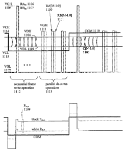
Figure 11 shows a representative timing diagram for an embodiment
of the present invention with a three level row driver. In the panel's initial
state, the row lines RA[M-1:0] 1100 and RB[M-1:0] 1101 are held in a low
voltage state as to prevent charge leakage from substantially all of the pixel
array's charge storage capacitors (i.e. at least one of every pixel's M1 904
or
M2 905 TFTs is in an "off" state). Generally this is accomplished by holding
all row lines (RA[M-1:0] 1100 and RB[M-1:0] 1101) at a low gate voltage
level, VGL 1102.
To perform a frame write operation, the column lines C[N-1:0] 1103
are driven to the desired pixel voltages for a given row of pixels. For the
present example, a bi-level column drive waveform using two data voltages,
VDH 1104 and VDL 1105 will be used to simplify the description and
drawings. Those skilled in the art will recognize that the column lines can be
driven with analog voltages between VDH 1104 and VDL 1105 to create a
grayscale response in the LCD material. The present teachings can be
generally applied to binary, multilevel and/or continuous analog column line
drive.
The two or more row select lines for a given row of pixels (e.g. RAm
1106 and RBm 1107) are then pulsed from their resting low voltage VGL 1102
to a high voltage VGH 1108 which has the effect of turning "on" all of the M1
904 and M2 905 TFTs in each of the pixels in an entire row of pixels. This
CA 02758803 2011-10-13
WO 2010/119113 PCT/EP2010/054994
19
selected row of pixels then charges to the voltages driven on the C[N-1:0]
700 800 1103 column lines. Once sufficient time has elapsed for the pixel
values Pm,n 909 1109 to substantially settle to the C[N-1:0] 1103 voltage
levels, the row select lines RAm 1106 and RBm 1107 are returned to their
resting low potential VGL 1102, turning "off' all of the M1 904 and M2 905
TFTs in the now de-selected row.
In a preferred embodiment, the voltage level VGL 1102 is chosen to
be negative enough so that the pixel charge stored on CST 907 does not
substantially leak away through M1 904 or M2 905 between pixel writes or
refreshes. The pixel storage capacitors CST 907 are preferably large enough
to prevent pixel charge leakage during non-selected periods and to overcome
(to the extent desired by the display designer) the residual image effect that
can occur on a pixel gray level transition due to the variable LCD capacitance
CLC 906. In this manner the voltage across the LCD pixels can be
independently programmed to generate a desired optical state of the array of
pixels by controlling the voltages across the liquid crystal cells. Each row
of
pixels can be similarly loaded to complete the frame as described above.
Those skilled in the art will recognize that the exact sequence of the actions
taken, e.g. that the rows are processed sequentially, can be modified to
achieve a similar end. Such modifications are considered within the scope of
the present teachings.
Referring to Figure 11, the COM electrode 1110 can optionally be
driven with an AC waveform to improve cell retention, limit array or source
voltage ranges and/or reduce system power as is well known in the art.
Figure 11 specifically gives the example of bi-level modulation between a
high value VCH 1114 and a low level VCL 1115. The present teachings
regarding low frame rate operation of TFT pixels incorporating negative
stress mitigation through gate modulation can be applied by one skilled in the
art to the many known methods of COM modulation and/or applied without
limitation to the case where COM 1110 is kept at a static DC voltage.
Once the entire array of pixel values is written, the array can be
CA 02758803 2011-10-13
WO 2010/119113 PCT/EP2010/054994
placed in a standby state to conserve power until the array of pixel voltages
Pm,n 909 leak away enough to require refreshing to prevent image artifacts
(e.g. flicker). This standby state between frame image write operations
comprises the second phase of the operation of a preferred embodiment.
5 Many applications of flat panels can make use of a variable frame rate; the
concepts described herein are well suited to applications where the frame
rate must run fast for certain types of content (e.g. 30Hz frame rate when the
user is actively interacting with the device) but also needs a low power state
where frame refresh rate can drop to a few Hz. To achieve this, a variable
10 length standby state can be inserted between the active frame writes or
refreshes of the first phase described above.
Referring to Figure 11, in a preferred embodiment of the present
invention, during the standby state in between frame write operations, the row
gate lines RAm 1106 and RB n 1107 for a given row, a subset of rows or all the
15 rows are alternately biased between a "off" state with gate voltage VGL
1102
and a weak "on" state with a gate voltage VGM 1111 which is chosen to
preferably achieve a slightly positive VGS across the pixel transistors M1 904
and M2 905. When the pixel is in such a bias state (i.e. either but not both
of
M1 904 and M2 905 in a weakly "on" state) the pixel charge that was written
20 during the frame write operation is substantially preserved. The
application of
the weakly "on" gate bias VGM 1111 to a TFT injects any accumulated
positive charges (i.e. holes) that arose during the previous "off" state which
has the effect of reducing the average charge density in the TFT channel
which thus interrupts the negative stress accumulation of the TFT device.
This operation of the two pixel TFTs 904 905 in an opposing state (e.g. on/off
or off/on) is herein referred to as a de-stress operation and is
preferentially
performed in sequence with or interleaved with frame or line refreshes to
minimize negative bias stress and/or power dissipation of the display. A
substantial number of de-stress operations can be inserted between or
interleaved within frame refreshes to significantly reduce the negative stress
accumulation.
CA 02758803 2011-10-13
WO 2010/119113 PCT/EP2010/054994
21
In a preferred embodiment of the present teachings the gate voltages
on the pixel transistors M1 904 and M2 905 employ a "break before make"
switching transition during the de-stress operation; this ensures that the
pixel
charge on CST 907 is well protected against rise/fall time variations and
charge leakage at the gate voltage transitions of M1 904 and M2 905.
In a preferred embodiment of the present teachings, all of the RA[M-
1:0] 1100 lines in the display are pulsed to VGM 1111 at substantially the
same time while the RB[M-1:0] lines 1101 are all held in an "off" state at a
negative gate voltage VGL 1102. By pulsing in parallel a large number of
row lines, the row driver circuit in the driver IC 603 can be designed to
expend
less energy using techniques known in the art as charge sharing, stepwise
charging, staircase charging or adiabatic charging methods. As a result, the
parallel de-stress operation of alternately pulsing all RA[M-1:0] 1100 and
RB[M-1:0] 1101 lines can be implemented with substantially better power
efficiency compared to sequential switching or pulsing of single gate lines.
By inserting additional AC modulation of the TFT array transistors in
excess of the frame write rate, the TFT bias stress is substantially reduced
at
low frame write rates. Since the energy required to pulse many row lines to a
weakly "on" state can be substantially less than that required for a full
frame
refresh, the power dissipation of the panel as a whole can be reduced
significantly without incurring the short lifetime penalty of low frame rate
refresh in conventionally scanned TFT displays.
Figure 11 specifically shows a well differentiated frame write operation
1112 and a number (three) of parallel de-stress operations 1113 between
successive frame write operations. Persons skilled in the art will recognize
that a wide variety of scanning waveforms that transpose, interleave, group,
sequence or otherwise reorder the two basic display drive operations of the
present teachings, namely writing a pixel in one operation and subsequently
de-stressing the pixel in another operation. The scope of the claims is not
limited by such modifications or permutations. In some cases, for example, it
may be advantageous to interleave the de-stress and write operations so that
CA 02758803 2011-10-13
WO 2010/119113 PCT/EP2010/054994
22
a de-stress operation is applied after only a subset of the rows are written.
Those skilled in the art will recognize that the exact sequence of the actions
taken, e.g. that the rows are processed sequentially, can be modified to
achieve a similar end. Some advantageous changes, e.g. writing all even
rows first, then all odd rows, and/or partial display refresh can be adapted
to
the present system to reduce voltage swings and power dissipation by
minimizing transitions while performing any number of inversion techniques,
including line, column, frame and dot inversion DC balancing. Such
modifications and permutations are considered within the scope of the
present teachings.
In a preferred embodiment of the present teachings, the voltage
levels VGL, VGM and VGH are chosen to obey the following relationship:
VGH > VGM > VGL. Persons skilled in the art will recognize that the timing
and voltage levels chosen to implement the write process and de-stress
process can be adjusted and modified to meet specific engineering
requirements; the scope of the claims is not limited by such adjustments and
modifications.
Figure 12 shows a representative timing diagram of a preferred
embodiment of the present teachings similar to that of Figure 11 except that
it
utilizes a four level row drive signal with modified DC voltage levels. In
comparison with the waveforms of Figure 11, the low level VGL 1200 of the
row signals, RA[M-1:0] 1201 and RB[M-1:0] 1202 has been substantially
raised and is applied after a specific row is written during frame write
operation 1203 and during the standby state in between de-stress operations
1204. As shown in Figure 11, starting from the left side, the COM electrode
1205 transitions from VCH 1214 to VCL 1215 to start the new frame write;
substantially coincident with the COM 1205 transition, substantially all of
the
RA[M-1:0] 1201 and RB[M-1:0] 1202 lines are driven with a substantially
similar voltage step polarity and magnitude as the COM line 1205 to level
VGLL 1207. Since the stored pixel voltages in the array are strongly coupled
to COM 1205, the M1 904 and M2 905 gates are kept in an "off" state during
CA 02758803 2011-10-13
WO 2010/119113 PCT/EP2010/054994
23
this transition. The new frame is then scanned into the pixel array by
sequentially pulsing RAm 1208 and RBm 1209 lines to VGH 1210 to activate
each row of pixels while applying pixel data on column lines C[N-1:0] 1211 in
the form of data voltage levels VDH 1212 and VDL 1213. After pulsing to VGH
1210, the row lines RAm 1208 and RBm 1209 are brought back to the now
raised VGL 1200 level. Once all of the lines are scanned and the frame is
loaded (i.e. written or refreshed), all of the row lines will have been
returned to
the VGL 1200 level. De-stress operations that switch the two sets of RA[M-
1:0] 1201 and RB[M-1 :0] 1202 row lines alternately between VGL 1200 and
VGM 1216 are then inserted between frame write operations as in Figure 11.
When the COM 1205 is transitioned upward for the subsequent frame to
VCH 1214, the row lines RA[M-1:0] 1201 and RB[M-1:0] 1202 are
preferentially held at VGL 1200 as shown in Figure 12.
By transitioning all of the row lines from VGL 1200 to VGLL 1207 in
concert with the COM 1205 transition to VCL 1215, the negative stress on
the M1 904 and M2 905 TFTs is minimized. The leakage conduction in row
ESD circuits, e.g. 608 710 810 812, is also minimized by keeping the
voltage difference between the row signals RA[M-1:0] 1201, RB[M-1:0] 1202
and COM 1205 low. Note that the waveform of pixel voltage Pm,n 1217 is
substantially unchanged from that of Figure 11 Pm,n 1109 despite the lower
amplitude row signals. By applying a four level row drive, the row voltage
excursions from the COM level can be minimized in a COM modulation
technique to minimize ESD leakage power.
In a preferred embodiment of the present invention, the four levels
used for the row driver (VGH, VGM, VGL and VGLL) obey the following
relationship: VGH > VGM > VGL > VGLL. In a preferred embodiment of the
present invention the two levels of the column driver (VDH and VDL) and the
two levels of the COM driver (VCH and VCL) obey the following relationship:
VCH > VDH > VDL > VCL. In a preferred embodiment, the row voltages and
column voltages obey the following relationship: VGH > VDH > VDL > VGL.
In an additional embodiment (not shown), the transition in the gate
CA 02758803 2011-10-13
WO 2010/119113 PCT/EP2010/054994
24
line voltages when COM transitions can be implemented by floating the row
lines prior to the COM transition.
Since the row gate lines are strongly coupled to COM, they will substantially
follow the COM step with the desired amplitude and polarity. Additionally
when integrated a-Si row drivers are used, the output of the row driver can
be disconnected after the last de-stress operation and only re-connected
upon selection during the frame write when the selected row is driven to VGH
then VGL. In this fashion the waveforms of Figure 12 can be naturally
implemented with a floating row line drive technique, e.g. in a display
implementing an integrated row driver circuit made of a-Si TFTs that does not
have a high duty cycle pull down device on the row lines.
Figure 13 shows a representative timing diagram of a preferred
embodiment of the present teachings consisting of a four level row drive
signal and a four level column drive signal. The operation of the COM signal
1304 and row signals RA[M-1:0] 1305 and RB[M-1:0] 1306 is identical to the
description given for Figure 12. Comparing Figures 12 and 13, Figure 13 has
two additional voltage levels available for the column driver, VDHH 1300 and
VDLL 1301. These voltages are preferentially driven onto the column lines
during the frame write operation when the desired pixel is transitioning from
the opposite state (e.g. white to black or black to white). The voltage levels
VDHH 1300 and VDLL 1301 preferentially sit outside the normal range of
column source voltage (VDH 1302 and VDL 1303) and are chosen to
compensate for the time-varying capacitance of the liquid crystal upon an
optical state change. As is well known in the art, overdrive of the pixel on a
state change can allow the pixel voltage to settle to a more desirable final
value (e.g. to the values achieved by static pixels written repeatedly to VDH
1302 or VDL 1303) within the first frame. The bottom waveforms of Figure
13 show a the pixel voltage Pm,n 1307 being overdriven by the initial VDHH
1300 or VDLL 1301 levels but relaxing to the desired VDH 1302 or VDL 1303
cell voltage levels as the LC material slowly responds to the new optical
state.
Such overdrive techniques that can mitigate residual image or image sticking
CA 02758803 2011-10-13
WO 2010/119113 PCT/EP2010/054994
problems can optionally be applied to the present teachings without limiting
the present claims.
In a preferred embodiment of the present invention represented in
the waveforms of Figure 13, the four levels of the column driver (VDHH,
5 VDH, VDL and VDLL) obey the following relationship: VDHH > VDH > VDL >
VDLL. The choice of voltage levels for each of the four column levels
described in Figure 13 can be similarly modified to share levels with other
voltages available in the system (e.g. VCH, VCL) to reduce the number of
independent power supplies required by the display. The scope of the claims
10 is not limited by such choices or optimizations.
Figure 14 shows the operational flow chart of this embodiment.
Starting from the top of Figure 14, the first decision process 1400 determines
the polarity the present frame. If the last frame polarity was with COM=low,
the COM modulation high operation 1402 is performed wherein COM is
15 driven to VCH and all of the row lines RA[M-1:0] and RB[M-1:0] held at VGL.
If the last frame polarity was with COM=high, the COM modulation low
operation 1401 is performed wherein COM is driven to VCL and all of the row
lines RA[M-1:0] and RB[M-1:0] are driven to VGLL. Next, a row write
operation 1403 comprises driving the C[N-1:0] column lines to the desired
20 pixel voltages or desired overdriven pixel voltages for a given row,
driving a
selected pair of row lines RAm and RBm to VGH to capture the column
voltages into a selected row of pixel storage capacitors and finally returning
the selected pair of row lines to VGL. A decision process 1404 implements a
loop with row write operation 1403 wherein upon exit all of the rows have
25 been written with the selected polarity pixel voltages. Note that midway
through the frame write sequence of the COM=low frame (i.e. the loop of row
writes formed by 1403 and 1404), some fraction of row lines RA[M-1:0] and
RB[M-1:0] will be at VGL and the balance will be at VGLL.
Next, the first de-stress operation 1405 applies VGM to all RA[M-1:0]
signals then returns RA[M-1:0] to VGL followed by the second de-stress
operation 1406 which applies VGM to all RB[M-1:0] signals then returns
CA 02758803 2011-10-13
WO 2010/119113 PCT/EP2010/054994
26
RB[M-1:0] to VGL. A delay operation 1407 wherein all of RA[M-1:0] and
RB[M-1:0] are held at VGL completes the three phase de-stress operation
(i.e. the combination of steps 1405,1406 and 1407). Note that the sequence
of events (de-stress all Ml s first by pulsing RA[M-1:0], then all M2s by
pulsing RB[M-1:0], then delay) can be arbitrarily sequenced, reordered,
spliced with additional delays, repeated, exited at any operation, and/or
interleaved within the scope of the present teachings. For example, de-
stressing the RB[M-1:0] signals can be done first. In another example, the
frame write operation can be broken up into one or more sections (partial
frame updates of one or more rows) that are then interleaved with de-stress
operations and/or delays. In an additional embodiment (not shown) portions
of the pixel frame can remain undriven (frame write operation only updates
part of the frame) to conserve additional energy as well. Such
implementation decisions are compatible with the present teachings and can
benefit from the stress mitigation and low power techniques embodied
herein.
Referring again to Figure 14, once the desired number of de-stress
operations has been completed, the final decision process 1408 exits the de-
stress loop formed by 1405,1406, 1407 and 1408 and returns to the first
decision process 1400 to start a subsequent opposite polarity frame.
The waveforms and operations described in Figures 11 through 14
can be synthesized using a variety of well know techniques. In a preferred
embodiment, DC voltage sources and switch based multiplexors are
controlled digitally to generate the multilevel waveforms of Figures 11
through 13. For example, the row waveforms of Figure 11 use a three level
row driver that selects between VGL, VGM and VGH. For the column
waveforms of Figures 11 and 12, a two level analog mux is required that
selects between VDH and VDL DC levels. Similarly COM requires a two level
mux that selects between VCH and VCL.
One skilled in the art will recognize a number of different generation
mechanisms including DACs followed by buffer amplifiers, bootstrapped
CA 02758803 2011-10-13
WO 2010/119113 PCT/EP2010/054994
27
charge pumps, alternate demultiplexing circuits, etc. that can be used to
synthesize similar waveforms. Such alternate waveform synthesis methods
are well known in the art and can be substituted without impacting the utility
of
the present teachings.
Figure 15 shows a preferred embodiment of the present teachings
incorporating a hierarchical multiplexer arrangement that improves power
efficiency during de-stress operations. Source mux 1500 generates an
intermediate signal DSA 1501 and source mux 1502 generates an
intermediate signal DSB 1503 by selecting from the desired endpoint de-
stress DC levels VGM 1504 and VGL 1506 as well as any number of
intermediate voltage levels 1505. The COM mux 1526 generates the COM
signal 1529 by selecting between VCH 1527 and VCL 1528. The
intermediate signals DSA 1501 and DSB 1503 as well as two other DC
levels, VGH 1508 and VGLL 1507, form a bus 1509 that is connected to a
large number (e.g. 2M where M = number of pixel rows) of three-to-one
output muxes 1525 that in turn drive the row signals of the TFT display pixel
array 602 and row line ESD circuits 608.
Referring to Figure 15, prior to a frame write operation, all of the row
outputs RA[M-1:0] andRB[M-1:0] (e.g. RAo 1514, RBo 1516, RA, 1518, RB,
1520 through RAM_, 1522 and RBM_, 1524) are attached through their
respective muxes to either DSA 1501 or DSB 1503 which in turn are
connected to VGL 1506 by muxes 1500 and 1502. If the new frame is with
COM = VCH, 1527 then the row output muxes 1525 continue to select either
DSA 1501 or DSB 1503. However if the frame polarity requires COM = VCL
1528 then the row output muxes are driven to select VGLL 1507 as the
output. Thus for the COM = VCL 1528 polarity frame all the rows RA[M-1:0]
and RB[M-1:0] are driven to VGLL 1507 in concert with the transition on
COM 1529 as shown in Figures 12 and 13.
Referring again to Figure 15 specifically and Figures 12 through 14
generally, the next operation is the row-by-row writing of the frame which
comprises sequential pulsing of pairs of row lines, e.g. RAo 1514 and RBo, to
CA 02758803 2011-10-13
WO 2010/119113 PCT/EP2010/054994
28
a high level VGH 1508. Once a pair of row lines (e.g. RAo 1514 and RBo
1516) has been pulsed to VGH 1508 to write that specific row of pixels, the
selected pair of RAm and RBm signals are then connected to DSA 1501 and
DSB 1503 respectively through the appropriate output mux 1525. DSA 1501
and DSB 1503 are in turn held at VGL 1506 by muxes 1500 and 1502 so that
the now de-selected row lines RAm and RBm are driven to VGL 1506. Once
the entire frame has been written, none of the muxes 1525 remain attached
to VGH 1508 or VGLL 1507; all have transitioned to either DSA 1501 or DSB
1503 (and therefore voltage level VGL 1506) in preparation for the de-stress
operation.
Referring again to Figure 15 specifically and Figures 12 through 14
generally, the frame write operation is followed by one or more de-stress
operations which start with all of the output muxes 1525 selected so that the
output row lines RA[M-1:0] are attached to DSA 1501 and that the output row
lines RB[M-1:0] are attached to DSB 1503. When a de-stress operation is
performed, in the case where the RA[M-1:0] lines are de-stressed first, the
mux 1500 is digitally driven to sequentially select progressively increasing
voltages from VGL 1506, through the intermediate levels 1505 until reaching
VGM 1504. By driving the row driver outputs in small increments by selecting
sequentially and progressively from a set of efficiently generated
intermediate
power supplies 1505, the dissipated power of the circuit can be substantially
reduced, ideally by 1/(Q+1) where Q is the number of intermediate levels
1505. Since the de-stress operations preferentially drive the entire display
(e.g. all RA[M-1:0] are driven at the same time) the capacitive load seen on
DSA 1501 or DSB 1503 can be quite high (M row capacitances in parallel).
Furthermore, the de-stress operations do not preferentially have very
stringent requirements for rise and fall times. Both of these factors (large
capacitive load, rise/fall time not critical) make possible a fine-grain
adiabatic
or step-wise driving method to save substantial power. Note the intermediate
power supplies should be generated as efficiently as possible to maximize
the power savings.
CA 02758803 2011-10-13
WO 2010/119113 PCT/EP2010/054994
29
Figure 16 shows a representative step-wise driving of DSA 1501
1600 and DSB 1503 1601 from a starting low level VGL 1602 to a high level
VGM 1603 stepping at a number of efficiently generated intermediate power
supply voltages 1604.
Figure 17 shows a representative transfer curve of a TFT device 1700
with source (S), gate (G) and drain (D) terminals at the upper end of the
operating temperature range. As the voltage between the gate (G) and
source (S) (VGS 1702) is increased from very negative on the left, the drain-
source current (IDS 1701) first falls then rises rapidly around VGS - 0
(following
curve 1703) and finally saturates at high positive VGS 1702. There is often
an optimum VGS 1702 voltage at which the "off' conduction is minimized, e.g.
1704.
Reviewing the waveforms of Figure 11, it can be seen that in the
case where row line resting voltage during de-stress (i.e. VGL 1102), the
voltage of the CS lines (VDH 1104 and VDL 1105) and the voltage on the
pixels (Pm,n 1109, in the range of VDH 1104 and VDL 1105) creates a more
negative VGS operating point 1705 than the ideal operating point 1704. This
is because VGL 1102 in the drive scheme of Figure 11 must be chosen that it
is low enough to prevent the pixel TFTs from turning partially "on" when COM
1110 transitions to VCL 1115 (pixel voltages Pm,n 1109 are capacitively driven
lower by COM and the gate lines of the pixel transistors must be low enough
to prevent conduction). But such a low gate level, when applied continuously
as the resting state for row lines between other operations, creates non-
optimum leakage conduction (e.g. operating point 1705) in the pixel TFTs.
For example a 50% increase in leakage current (e.g. the difference 1706
between operating points 1704 and 1705) will have the undesirable effect of
causing the stored pixel voltages, Pm,n 1109, to leak away 50% faster than
they otherwise could (i.e. if they were at optimal VGS 1702 point 1704). To
compensate, the frame rates and storage capacitor sizes must be increased
which will adversely affect power. Furthermore, since the low gate voltage
VGL 1102 in Figure 11 is substantially different from COM 1110 (especially in
CA 02758803 2011-10-13
WO 2010/119113 PCT/EP2010/054994
the COM = VCH 1114 frame polarity) the power dissipation in the ESD
structures, e.g. 608 710 810 812, which provide a nonlinear conduction path
from row lines to COM 1110 can become prohibitive.
In contrast, the waveforms of Figures 12 and 13, the flow diagram of
5 Figure 14 and the multiplex based driver IC circuit of Figure 15 circumvent
this limitation by introducing a four level row waveform that keeps the VGS
1702 of the pixel array at or near the optimum operating point 1704 for the
majority of either polarity frame. This allows further reduction in frame rate
and/or storage capacitance to save additional power. Furthermore, since the
10 row signals of Figures 12 and 13 are driven with less voltage difference to
COM, the ESD structure leakage power (which is highly nonlinear in voltage)
is also substantially reduced.
Additionally, since the channel charge accumulation rate is slowest at
the optimum "off" VGS 1704 (i.e. charge carriers, e.g. holes, accumulate more
15 slowly at operating point 1704 versus operating point 1705), the frequency
dependence of the negative stress on the pixels shifted lower using the
waveforms of Figures 12 and 13, allowing frame write operation rate and de-
stress operation rate to be further reduced saving additional power. Also,
since the magnitude of the negative Vas during the "off' time in Figures 12
20 and 13 is reduced, the power-law dependence on voltage of the negative
bias stress accumulation is minimized as well. Thus the present teachings
provide substantial improvements in both display module power and device
reliability.
Figure 18 shows an electronic shelf label 1802 integrating the flat
25 panel display 1803 of the present teachings into a device that can be
attached to a store shelf 1800 to display product information and pricing. An
interactive button 1801 can be used to provide additional information to store
personnel or shoppers.
Figure 19 shows a shopping cart handlebar mounted display utilizing
30 the present teachings. A display 1901 is attached to a shopping cart
handlebar 1900. One or more buttons or a keypad 1902 allows for user
CA 02758803 2011-10-13
WO 2010/119113 PCT/EP2010/054994
31
input.
Figure 20 shows an electronic book design utilizing the present
teachings. The electronic book 2000 is comprised of a low power screen
2001 and a navigation keypad 2002.
Figure 21 shows a clamshell cell phone design utilizing the present
teachings. A low power reflective outer screen 2101 is integrated into the lid
of the cell phone 2100.
Figure 22 shows a portable digital music player 2200 integrating a
display 2201 based on the present teachings.
Figure 23 shows a computer monitor, promotional signage or
television 2301with a display 2300 based on the present teachings.
Figure 24 shows a portable computer, digital picture frame or
portable DVD player 2400 with a display 2401 based on the present
teachings. Such a screen 2401 based on the present teachings can be
integrated inside or outside the clamshell (not shown) or the design can be
without a hinge (not shown).
Figure 25 shows an outdoor or indoor digital billboard comprised of
one or more sub-displays 2500 utilizing the present teachings. Optional front
lights 2501 provide sufficient illumination for nighttime readability.