Note: Descriptions are shown in the official language in which they were submitted.
CA 02769121 2012-01-24
WO 2011/015206 1 PCT/EP2009/005609
HIGHLY EFFICIENT CMOS TECHNOLOGY COMPATIBLE SILICON
PHOTOELECTRIC MULTIPLIER
FIELD OF THE INVENTION
The invention relates to the field of semiconductor opto-
electronic devices, particularly to photodetectors with high
efficiency of light detection, including the visible part of
the spectrum. The photodetectors according to the invention
can be used in a wide field of applications, which employ the
detection of very weak and fast optical signals as, for exam-
ple, industrial and medical tomography, life science, nu-
clear, particle and astroparticle physics etc.
BACKGROUND OF THE INVENTION
The device for single-photon detection is known as a Single
Photon Avalanche Detector-SPAD [e.g. "Avalanche photodiodes
and quenching circuits for single-photon detection", S. Cova,
M. Ghioni, A. Lacaita, C. Samori and F. Zappa in APPLIED
OPTICS vol. 35 No. 12, 20 April 1996, and E. Sciacca, A. Gi-
udice, D. Sanfilippo, F. Zappa, S. Lombardo, R. Concentino,
C. Di Franco, M. Ghioni, G. Fallica, G. Bonanno, S. Cova, E.
Rimini "Silicon Planar Technology for Single-Photon Optical
Detectors", IEEE Transactions on electron devices, vol. 50,
No.4, April 2003], the known device comprises a silicon sub-
strate with an epitaxial layer made on it, said layer having
on a surface a small (10-200 microns) region (a cell) of con--
ductive type that is opposite to the given layer conductive
type. The cell is supplied with reverse bias that exceeds
breakdown voltage. When a photon is absorbed in this region
the Geiger discharge takes place, said discharge is limited
with an external quenching resistor.
CA 02769121 2012-01-24
WO 2011/015206 2
PCT/EP2009/005609
Such a single-photon detector (SPAD) has a very small area or
volume, and also it is not able to measure the light flux in-
tensity.
In order to eliminate these defects it is necessary to use a
large number (= 103) of such cells located on a common sub-
strate having an area equal to or larger than 1 mm2. In this
case each cell works as the above described photon detector
and the device as a whole detects light intensity that is
proportional to the number of the worked cells.
Such type of device - the Silicon Photomultiplier(SiPM) - is
described in patent RU 2004113616 with a priority 05.05.2004
and European Patent Application EP 1 755 171 Al, pub.
21.02.2007 "Silicon Photomultiplier (variants) and cell
therefore" - and accepted as the nearest prior art for pres-
ent invention. The SiPM comprises a silicon substrate, a plu-
rality of cells the sizes of which are 20-100 microns and
which are located on a surface of said substrate in an epi-
taxial layer; each cell has an internal individual quenching
resistor made of high resistance polysilicon and located on
top of the silicon oxide layer which covers all cells. The
main defects of this device are the following:
= the usage of high resistance polysilicon quenching resis-
tors which is not CMOS-technology compatible;
= the location of polysilicon quenching resistors on top of
= the silicon oxide layer requires the opening of many (-
few x 103) windows in silicon oxide layer for connection
of quenching resistor with entrance window silicon layer
of the SiPM - that leads to the loss of the photon detec-
tion efficiency (PDE) and makes the fabrication process
more complicate;
= the presence of epitaxy layer gives rise to the increasing
of dark rate of the SiPM and also makes the fabrication
process more complicate.
CA 02769121 2013-12-17
3
It is therefore an object of the present invention to provide
a cell for a silicon-based photoelectric multiplier which is
easy and efficient to fabricate and at the same time
comprises a high efficiency of light detection in operation.
The present invention provides a cell for a silicon based
photodetector having high efficiency in a broad band of
wavelengths with a coefficient of amplification up to 107 due
to increased cell sensitiveness and significantly reduced
dark rate - all that achieved within the framework of CMOS
technology. The present invention also provides a silicon
based photodetector comprising a plurality of such cells.
One essential idea of the present invention is the fact that
the quenching resistor in the cell of the silicon-based
photoelectric multiplier is formed essentially in an
uppermost layer of the semiconductor body or in other words
laterally besides the upper layer of the p-n junction of the
device. The quenching resistor layer is thus comprised of a
semiconductor layer which is connected to a lateral side face
of the upper layer of the p-n junction and which extends in a
direction away from the p-n junction to connect the p-n
junction with a voltage distribution line. The quenching
resistor layer, for example, can be fabricated as a well area
in the upper surface of the semiconductor body comprising a
dopant concentration in order to yield a desired resistance
or resistivity value in order to function as a quenching
resistor for quenching the avalanche current. The invention
therefore allows to integrate the fabrication of the
quenching resistor layer within a CMOS fabrication process.
CA 02769121 2012-01-24
WO 2011/015206 4 PCT/EP2009/005609
According to an embodiment also the voltage distribution lay-
ers or lines can be integrated within the CMOS fabrication
process. The voltage distribution lines can also be fabri-
cated as well areas into the upper surface of the semi-
conductor body, these well areas comprising comparably high
dopant concentration to function as electrically conductive
lines.
A method of fabricating a silicon-based photoelectric multi-
plier such as that shown in embodiments of Figs. 2 and 3
could be performed in the form of a complete CMOS fabrication
process wherein the fabricating of all layers which are of
functional significance of the device would be integrated in
the CMOS fabrication process. In particular the process would
comprise the steps of providing a silicon substrate, fabri-
cating a first layer of a first conductivity type, fabricat-
ing a plurality of second layers of a second conductivity
type, and fabricating a plurality of quenching resistor lay-
ers and voltage distribution lines, all fabrication steps be-
ing conducted preferably by ion implantation processes.
Moreover a buried layer of a first conductivity type could be
fabricated by a deep ion implantation process.
BRIEF DESCRIPTION OF THE DRAWINGS
The accompanying drawings are included to provide a further
understanding of embodiments and are incorporated in and con-
stitute a part of this specification. The drawings illustrate
embodiments and together with the description serve to ex-
plain principles of embodiments. Other embodiments and many
of the intended advantages of embodiments will be readily ap-
preciated as they become better understood by reference to
the following detailed description.
CA 02769121 2012-01-24
WO 2011/015206 5 PCT/EP2009/005609
Fig. 1A,B shows a top view representation (A) and a cross-
sectional representation (B) of a cell of a silicon-based
photoelectric multiplier according to an embodiment;
Fig. 2 shows a top view representation of a section of a
silicon-based photoelectric multiplier according to an em-
bodiment;
Fig. 3 shows a cross-sectional representation along line A-A
of Fig. 2 of the silicon-based photoelectric multiplier ac-
cording to an embodiment.
DETAILED DESCRIPTION OF THE INVENTION
The aspects and embodiments are now described with reference
to the drawings, wherein like reference numerals are gener-
ally utilized to refer to like elements throughout. In the
following description, for purposes of explanation, numerous
specific details are set forth in order to provide a thorough
understanding of one or more aspects of the embodiments. It
may be evident, however, to one skilled in the art that one
or more aspects of the embodiments may be practiced with a
lesser degree of the specific details. In other instances,
known structures and elements are shown in schematic form in
order to facilitate describing one or more aspects of the em-
bodiments. The following description is therefore not to be
taken in a limiting sense, and the scope is defined by the
appended claims. It should also be noted that the representa-
tions of the various layers, sheets or substrates in the Fig-
ures are not necessarily to scale.
In the following detailed description, reference is made to
the accompanying drawings, which form a part thereof, and in
which is shown by way of illustration specific embodiments in
which the invention may be practiced. In this regard, direc-
CA 02769121 2012-01-24
WO 2011/015206 6 PCT/EP2009/005609
tional terminology, such as "upper", "lower", "left-hand",
"right-hand", "front side", "backside", etc., is used with
reference to the orientation of the Figure(s) being de-
scribed. Because components of embodiments can be positioned
in a number of different orientations, the directional termi-
nology is used for purposes of illustration and is in no way
limiting. It is to be understood that other embodiments may
be utilized and structural or logical changes may be made
without departing from the scope of the present invention.
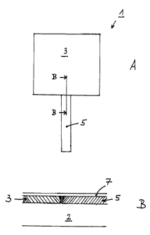
Fig. lA shows a top view representation of a cell of a sili-
con-based photoelectric multiplier according to an embodiment
and Fig. 1B shows a cross-sectional representation of the
cell along line B-B of Fig. 1A.
The cell 1 comprises a layer 2 of a first conductivity type
and a layer 3 of a second conductivity type formed on the
layer 2 so that the layer 2 and the layer 3 form a first p-n
junction. The cell 1 further comprises a quenching resistor
layer 5 formed on the layer 2 laterally besides the layer 3
and connected to a lateral side face of the layer 3.
The cell 1 and in particular the layer 3 can have a rectangu-
lar or quadratic shape and the quenching resistor layer 5 can
be connected to one of the side edges of the layer 3, in par-
ticular in the center of the side edge. The quenching resis-
tor layer 5 extends in a direction away from the layer 3 to
make electrical contact to a voltage distribution line (not
shown) remote from the layer 3. The cell 1 can also comprise
an insulation layer 7 covering the layer 2, the layer 3 and
the quenching resistor layer 5. The insulation layer 7 can be
such that it covers the whole matrix of cells with only one
opening at an edge portion of the device for the purpose of
electrically contacting the voltage distribution line. The
layer 3 and the quenching resistor layer 5 can be formed as
well areas into the layer 2 by using conventional ion implan-
CA 02769121 2012-01-24
WO 2011/015206 7 PCT/EP2009/005609
tation processes as known in CMOS fabrication technology. As
can be seen in Fig. 1B, the implantation region of the layer
3 is shown left-hatched and the implantation region of the
quenching resistor layer 5 is shown right-hatched and an
overlap between both regions can be provided when conducting
the implantation steps so as to provide for a satisfactory
electrical contact between both regions.
It is to be noted that the elements as shown in Fig. lA are
not necessarily to scale as regards their dimensions with re-
spect to each other as well as the geometric dimensions of
the elements themselves. For example the quenching resistor
layer 5 is shown to have a strip-like shape wherein the
strip-like quenching resistor layer 5 can have, for example,
a length to width ratio of greater than 10, more preferably
greater than 20, more preferably greater than 30. Moreover
the ratio of the length of a side edge of the cell 1 or of
the layer 3 to the width of the strip-like quenching resistor
layer 5 can be, for example, greater than 10, more preferably
greater than 20, more preferably greater than 30.
Furthermore the quenching resistor layer 5 can have a resis-
tivity in the range of 10 to 50 KOhm/square. With such a re-
sistivity the quenching resistor layer 5 can efficiently act
as a quenching resistor for quenching the avalanche current
in operation of the photodiode. The value of the resistivity
can be adjusted by the geometric dimensions and the dopant
concentration of the quenching resistor layer 5.
The layer 3 can have a relatively high level dopant concen-
tration which can, for example, be in the range of 1018 to
1019 cm-3.
CA 02769121 2012-01-24
WO 2011/015206 8 PCT/EP2009/005609
Fig. 2 shows a top view representation of a section of a
silicon-based photoelectric multiplier according to an em-
bodiment.
The photoelectric multiplier 10 depicted in Fig. 2 is com-
prised of a plurality of cells 1 such as that shown in Figs.
1A,B. They are arranged along rows wherein the cells 1 of one
row are laterally displaced with respect to the cells 1 of an
adjacent row wherein the displacement can be, for example,
half the length of one side edge of a quadratically shaped
cell 1.
The photoelectric multiplier 10 can have a plurality of volt-
age distribution lines 6. In the section of the photoelectric
multiplier 10 as shown in Fig. 2 there are shown two voltage
distribution lines 6 which are arranged along outer side
edges of two adjacent rows of cells 1. The quenching resistor
layers 5 of each cell 1 of one row extend in the narrow space
between two neighboring cells 1 of an adjacent row and are
electrically connected with the voltage distribution line 6
extending along the adjacent row. The voltage distribution
lines 6 can also be made of a well area formed within the
layer 2. In particular the voltage distribution lines 6 can
be formed of well areas having a dopant concentration of
about 1019 cm-3 or 5 x 1019 cm-3 to 5 x 1019 cm-3 so that they
function as conductive wires. Thus the fabrication of the
voltage distribution lines 6 can also be part of and embedded
within the CMOS fabrication process.
Also shown in the top view representation of Fig. 2 are the
grooves 4 which surround each one of the cells 1 and which
prevent the penetration of secondary Geiger photons from one
cell to the adjacent cells. The grooves 4 are shown in more
detail in an embodiment of a silicon-based photoelectric mul-
tiplier as shown in Fig. 3.
CA 02769121 2012-01-24
WO 2011/015206 9 PCT/EP2009/005609
Fig. 3 shows a cross-sectional representation along line A-A
of Fig. 2 of the silicon-based photoelectric multiplier ac-
cording to an embodiment.
The section of the photoelectric multiplier 20 shown in Fig.
3 includes the right part of one cell 1 shown on the left
side of the drawing and the left part of a further cell 1
shown on the right side of the drawing and a region in be-
tween the adjacent cells 1, the region comprising a quenching
resistor layer 5 and grooves 4. The photoelectric multiplier
comprises a substrate 21 of a second conductivity type
having a relatively low doping agent concentration which can
be, for example, in the range of 5 x 10¹³ - 5 x 1014 cm-3 and a
15 buried layer 22 of a first conductivity type having a peak
doping agent concentration in the range of 5 x 10¹⁷ - 5 x 10¹⁸
cm-3 and a gradient of doping concentration in the order of
1015- 1018 from up to down due to back scattering of im-
planted ions; such a gradient creates a built-in electric
20 field, said field forces carriers generated by yellow-red
photons in the doping gradient region to move into Geiger de-
pletion region to be detected. This leads to the increase of
long wavelength photon detection efficiency. The substrate 21
and the buried layer 22 form another N-P junction at an in-
terface between them.
Above the buried layer 22 the plurality of identical cells 1
with the grooves 4 as separating elements between them is lo-
cated, wherein each cell 1 is formed by the layer 2 and the
layer 3. The layer 2 is common for all cells 1 and it is con-
tiguous throughout the photoelectric multiplier 20. The layer
3 is formed as a thin layer of second conductivity type hav-
ing a relatively high doping agent concentration like, for
example, 1018 to 1018 cm-3, and disposed on top of the layer 2.
The layer 3 functions as an entrance window of the photoelec-
CA 02769121 2012-01-24
WO 2011/015206 10 PCT/EP2009/005609
tric multiplier 20. The layer 2 and the layer 3 form an N-P
junction at an interface between them, wherein in operation a
reverse bias voltage is applied to the N-P junction to such
an extent that the photodiode operates in the Geiger mode.
The thin strip-like silicon quenching resistor layers 5 of
second conductance type connect each cell 1 with one of the
voltage distribution lines 6 and serve as quenching resistors
having a resistance of 10 - 50 KOhm/square. The voltage dis-
tribution lines 6 are made of second conductivity type silt-
con layers having a relatively high doping agent concentra-
tion like, for example, about 1019 cm-3 or 5 x 1018 cm-3 to 5 x
1019 cm-3 of a doping agent concentration. The upper surface
of the photoelectric multiplier 20 is covered by an insula-
tion layer 7, in particular a silicon oxide layer, with cor-
responding antireflection properties at an upper surface
thereof. Said strip-like quenching resistor layers 5 and
voltage distribution lines 6 are disposed between the layer 2
and the insulation layer 7. The voltage distribution lines 6
are connected together on the periphery of the photoelectric
multiplier and there is only a single input power supply con-
tact through a single opening window in the insulation layer
7. Finally a grid-like aluminum layer 8 which is serving for
the output of the SiPM signal is disposed on top of the sili-
con oxide layer.
The photoelectric multiplier 20 according to Fig. 3 is an em-
bodiment of a highly efficient CMOS-technology compatible
photoelectric multiplier. The buried layer 22 can be formed
by an ion implantation step which can be carried out at an
appropriate time in the course of the CMOS fabrication proc-
ess. Also the other layers like the layer 3, the quenching
resistor layers 5 and the voltage distribution lines 6 can be
processed by further ion implantation steps at appropriate
times in the course of the CMOS fabrication process.
CA 02769121 2012-01-24
WO 2011/015206 11 PCT/EP2009/005609
The silicon based photoelectric multiplier 20 thus contains
the substrate 21 of the second conductivity type, the buried
layer 22 of the second conductivity type, a layer 2 of first
conductivity type, a layer 3 of second conductivity type
(entrance window), separation elements 4 (triangular grooves)
between the cells 1, strip-like quenching resistor layers 5
(quenching resistors) of first conductivity type, voltage
distribution buses 6, the insulation layer 7, and the grid-
like layer 8 on top of the insulation layer 7.
As an example, the substrate 21 can have p-type (n-type) con-
ductivity, the buried layer 22 can have n-type (p-type) con-
ductivity, the layer 2 can have n-type (p-type) conductivity,
the layers 3 can have p-type (n-type) conductivity, and the
quenching resistor layers 5 and the voltage distribution
lines 6 can have p-type (n-type) conductivity.
It should be noted further that according to the embodiment
of Fig. 3 the buried layer 22 is fabricated as a non-planar
layer, in particular it is fabricated such that it comprises
varying depth throughout the device. In Fig. 3 it can be seen
that in areas between the cells 1 the buried layer 22 is lo-
cated deeper within the substrate as compared to the areas of
the cells 1. The reason for this is that the electric field
will be higher within the cells 1 as compared to the areas
between the cells 1 so that only light which is incident on
the cell 1 will be efficiently detected only by cell 1.
The highly efficient light detection in a broad part of the
spectrum (300 nm - 700 nm) along with high uniformity of an
electrical field is reached in a structure as that shown in
Fig. 3, which is made by a CMOS-technology process. A high
electric field needed for Geiger-type discharge (voltage
above the breakdown value) is created in the N-P junction be-
tween the layer 3 (entrance window) and the layer 2.
CA 02769121 2012-01-24
WO 2011/015206 12 PCT/EP2009/005609
In addition in the embodiment of Fig. 3, another N-P junction
is made between the substrate 21 and the buried layer 22,
said junction preventing penetration of photoelectrons, cre-
ated by secondary photons of the Geiger discharge, into the
volume of adjacent cells. The penetration of the secondary
Geiger photons into the adjacent cells is also prevented by
the separating elements 4 between the cells which also serve
as optical barriers and which, for example, can be formed as
grooves, in particular triangular V-grooves.
Highly Efficient CMOS-technology compatible photoelectric
multipliers according to one of the above embodiments com-
prise independent cells having 20-100 microns of size, that
is, for example, length of one side edge of one cell 1 or
layer 3. All the cells are jointed through quenching resis-
tors 5 with voltage distribution buses 6, and the identical
bias voltage, exceeding the breakdown voltage, is applied to
the cells 1, that provides working in the Geiger mode. The
quenched Geiger discharge develops in the active region of
the cell when a photon gets there. The quenching, that is
stopping the discharge, takes place due to fluctuations of
the number of the charge carriers up to zero when the voltage
of the p-n boundary drops, due to availability of quenching
resistor 5 (current-limiting resistor) in each cell. The cur-
rent signals from the worked cells are summarized on a common
load. The amplification of each cell constitutes up to 107.
The spread of amplification value is defined by technological
spread of the cell capacity and breakdown voltage of the
cell, and constitutes less than 5%. As all the cells are
identical, the response of the detector to gentle light
flashes is proportional to the number of the worked cells,
i.e. to light intensity.