Note: Descriptions are shown in the official language in which they were submitted.
CA 02776292 2014-06-20
=
- 1
CLOSED-LOOP LOAD CONTROL CIRCUIT HAVING A WIDE OUTPUT RANGE
BACKGROUND OF THE INVENTION
Cross Reference to Related Applications
[00011 This application claims priority from commonly-assigned U.S.
Provisional Patent
Application No. 61/249,477, filed October 7, 2009, entitled LOAD CONTROL
DEVICE FOR A
LIGHT-EMITTING DIODE LIGHT SOURCE; U.S. Provisional Patent Application
No. 61/319,530, filed March 31, 2010; entitled LAMP DRIVER CONFIGURATION
DEVELOPMENT TOOL; U.S. Provisional Patent Application No. 61/332,983, filed
May 10, 2010,
entitled LOAD CONTROL DEVICE FOR A LIGHT-EMITTING DIODE LIGHT SOURCE and
U.S. Non-provisional Patent Application No. 12/814,026 filed June 11, 2010,
entitled CLOSED-
LOOP LOAD CONTROL CIRCUIT HAVING A WIDE OUTPUT RANGE.
Field of the Invention
100021 The present invention relates to a load control device for an
electrical load, and more
particularly, to an light-emitting diode (LED) driver having a load current
feedback circuit that
allows the LED driver to have a wide output current range.
Description of the Related Art
[0003] Light-emitting diode (LED) light sources are often used in place
of or as
replacements for conventional incandescent, fluorescent, or halogen lamps, and
the like. LED light
sources may comprise a plurality of light-emitting diodes mounted on a single
structure and provided
in a suitable housing. LED light sources are typically more efficient and
provide longer operational
CA 02776292 2012-03-30
WO 2011/044085 PCT/US2010/051405
- 2 -
lives as compared to incandescent, fluorescent, and halogen lamps. In order to
illuminate properly,
an LED driver control device (i.e., an LED driver) must be coupled between an
alternating-current
(AC) source and the LED light source for regulating the power supplied to the
LED light source.
The LED driver may regulate either the voltage provided to the LED light
source to a particular
value, the current supplied to the LED light source to a specific peak current
value, or may regulate
both the current and voltage.
[0004] The prior art dealing with LED drivers is extensive. See, for
example, the listing of
U.S. and foreign patent documents and other publications in U.S. Patent No.
7,352,138, issued
April 1, 2008, assigned to Philips Solid-State Lighting Solutions, Inc., of
Burlington, Massachusetts,
and U.S. Patent No. 6,016,038, issued January 18, 2000, assigned to Color
Kinetics, Inc., of Boston,
Massachusetts (hereinafter "CK").
[0005] LED drivers are well known. For example, U.S. Patent No.
6,586,890, issued
July 1, 2003, assigned to Koninklijke Philips Electronics N.V., of Eindhoven,
the Netherlands
(hereinafter "Philips"), discloses a driver circuit for LEDs that provide
power to the LEDs by using
pulse-width modulation (PWM). Other examples of LED drives are U.S. Patent No.
6,580,309,
published September 27, 2001, assigned to Philips, which describes switching
an LED power supply
unit on and off using a pulse duration modulator to control the mean light
output of the LEDs.
Moreover, the aforementioned U.S. Patent No. 6,016,038 also describes using
PWM signals to alter
the brightness and color of LEDs. Further, U.S. Patent No. 4,845,481, issued
July 4, 1989 to Karel
Havel, discloses varying the duty cycles of supply currents to differently
colored LEDs to vary the
light intensities of the LEDs so as to achieve continuously variable color
mixing.
[0006] Patent No. 6,586,890 also discloses a closed-loop current power
supply for LEDs.
Closed-loop current power supplies for supplying power to other types of lamps
are also well
known. For example, U.S. Patent No. 5,041,763, issued August 20, 1991,
assigned to Lutron
Electronics Co., Inc. of Coopersburg, Pennsylvania (hereinafter "Lutron"),
describes closed-loop
current power supplies for fluorescent lamps that can supply power to any type
of lamp.
[0007] U.S. Patent No. 6,577,512, issued June 10, 2003, assigned to
Philips, discloses a
power supply for LEDs that uses closed-loop current feedback to control the
current supplied to the
CA 02776292 2012-03-30
WO 2011/044085 PCT/US2010/051405
- 3 -
LEDs and includes means for protecting the LEDs. Likewise, U.S. Patent No.
6,150,771, issued
November 21, 2000, assigned to Precision Solar Controls Inc., of Garland,
Texas, and Japanese
patent publication 2001093662A, published 6 April 2001, assigned to Nippon
Seiki Co., Ltd.,
describe over-current and over-voltage protection for drivers for LEDs and
other lamps.
[0008] LED drivers that may be dimmed by conventional A.C. dimmers are
also known.
Thus, aforementioned U.S. Patent No. 7,352,138, and U.S. Patent No. 7,038,399,
issued
May 2, 2006, assigned to CK, describe LED-based light sources that are
controlled by conventional
A.C. phase control dimmers. The aforementioned U.S. Patent No. 6,016,038
discloses a PWM
controlled LED-based light source used as a light bulb that may be placed in
an Edison-mount
(screw-type) light bulb housing. Control of lamps, such as LED lamps, by phase
control signals are
also described in U.S. Patent No. 6,111,368, issued August 29, 2000, U.S.
Patent No. 5,399,940,
issued March 21, 1995, U.S. Patent No. 5,017,837, issued May 21, 1991, all of
which are assigned to
Lutron. U.S. Patent No. 6,111,368, for example, discloses an electronic
dimming fluorescent lamp
ballast that is controlled by a conventional A.C. phase control dimmer. U.S.
Patent No. 5,399,940
discloses a microprocessor-controlled "smart" dimmer that controls the light
intensities of an array
of LEDs in response to a phase control dimming voltage waveform. U.S. Patent
No. 5,017,837
discloses an analog A.C. phase control dimmer having an indicator LED, the
intensity of which is
controlled in response to a phase control dimming voltage waveform. The well-
known
CREDENZA in-line lamp cord dimmer, manufactured by Lutron since 1977, also
includes an
indicator LED, the light intensity of which is controlled in response to a
phase control dimming
voltage waveform.
[0009] Applications for LED illumination systems are also shown in U.S.
Patent
No. 7,309,965, issued December 18, 2007, and U.S. Patent No. 7,242,152, issued
July 10, 2007, both
assigned to CK. U.S. Patent No. 7,309,965 discloses smart lighting devices
having processors, and
networks comprising such smart lighting devices, sensors, and signal emitters.
U.S. Patent
No. 7,242,152 discloses systems and methods for controlling a plurality of
networked lighting
devices in response to lighting control signals. Such systems are also used in
the RADIORA
product, which has been sold since 1996 by Lutron.
CA 02776292 2012-03-30
WO 2011/044085 PCT/US2010/051405
-4-
100101 In addition, there are known techniques for controlling current
delivered to an LED
light source. LED light sources are often referred to as "LED light engines."
These LED light
engines typically comprise a plurality of individual LED semiconductor
structures, such as, for
example, Gallium-Indium-Nitride (GaInN) LEDs. The individual LEDs may each
produce light
photons by electron-hole combination in the blue visible spectrum, which is
converted to white light
by a yellow phospher filter.
[0011] It is known that the light output of an LED is proportional to the
current flowing
through it. It is also known that LEDs suffer from a phenomena known as
"droop" in which the
efficiency is reduced as the power is increased. For LEDs of the GaInN type
(used for providing
illumination), a typical load current is approximately 350 milliamps (mA) at a
forward operating
voltage of between three and four volts (V) which corresponds to approximately
a one watt (W)
power rating. At this power rating, these LEDs provide approximately 100
lumens per watt. This is
significantly more efficient than other conventional light sources. For
example, incandescent lamps
typically provide 10 to 20 lumens per watt and fluorescent lamps, 60 to 90
lumens per watt. As
discussed, LED light sources can provide larger ratios of lumens per watt at
lower currents, thus
avoiding the droop phenomena. Further, it is expected that, as technology
improves, the efficiency of
LED light sources will improve even at higher current levels than presently
employed to provide
higher light outputs per diode in an LED light engine.
[0012] LED light sources typically comprise a plurality of individual
LEDs that may be
arranged in both a series and parallel relationship. In other words, a
plurality of LEDs may be
arranged in a series string and a number of series strings may be arranged in
parallel to achieve the
desired light output. For example, five LEDs in a first series string each
with a forward bias of
approximately 3 volts (V) and each consuming approximately one watt of power
(at 350 mA through
the string) consume about 5 W. A second string of a series of five LEDs
connected in parallel across
the first string will result in a power consumption of 10 W with each string
drawing 350 mA. Thus,
an LED driver would need to supply 700 mA to the two strings of LEDs, and
since each string has
five LEDs, the output voltage provided by the LED driver would be about 15
volts. Additional
strings of LEDs can be placed in parallel for additional light output,
however, the LED driver must
be operable to provide the necessary current. Alternatively, more LEDs can be
placed in series on
CA 02776292 2012-03-30
WO 2011/044085 PCT/US2010/051405
- 5 -
each sting, and as a result, the LED driver must also be operable to provide
the necessary voltage
(e.g., 18 volts for a series of six LEDs).
[0013] LED light sources are typically rated to be driven via one of two
different control
techniques: a current load control technique or a voltage load control
technique. An LED light
source that is rated for the current load control technique is also
characterized by a rated current
(e.g., 350 milliamps) to which the peak magnitude of the current through the
LED light source
should be regulated to ensure that the LED light source is illuminated to the
appropriate intensity and
color. In contrast, an LED light source that is rated for the voltage load
control technique is
characterized by a rated voltage (e.g., 15 volts) to which the voltage across
the LED light source
should be regulated to ensure proper operation of the LED light source.
Typically, each string of
LEDs in an LED light source rated for the voltage load control technique
includes a current balance
regulation element to ensure that each of the parallel legs has the same
impedance so that the same
current is drawn in each parallel string.
100141 In addition, it is known that the light output of an LED light
source can be dimmed.
Different methods of dimming LEDs include a pulse-width modulation (PWM)
technique and a
constant current reduction (CCR) technique. Pulse-width modulation dimming can
be used for LED
light sources that are controlled in either a current or voltage load control
mode. In pulse-width
modulation dimming, a pulsed signal with a varying duty cycle is supplied to
the LED light source.
If an LED light source is being controlled using the current load control
technique, the peak current
supplied to the LED light source is kept constant during an on time of the
duty cycle of the pulsed
signal. However, as the duty cycle of the pulsed signal varies, the average
current supplied to the
LED light source also varies, thereby varying the intensity of the light
output of the LED light
source. If the LED light source is being controlled using the voltage load
control technique, the
voltage supplied to the LED light source is kept constant during the on time
of the duty cycle of the
pulsed signal in order to achieve the desired target voltage level, and the
duty cycle of the load
voltage is varied in order to adjust the intensity of the light output.
Constant current reduction
dimming is typically only used when an LED light source is being controlled
using the current load
control technique. In constant current reduction dimming, current is
continuously provided to the
CA 02776292 2012-03-30
WO 2011/044085 PCT/US2010/051405
- 6 -
LED light source, however, the DC magnitude of the current provided to the LED
light source is
varied to thus adjust the intensity of the light output.
[0015] Therefore, there is a need to provide an LED driver that is
flexible and configurable,
such that it can be used with LED light sources that are rated to operate at
different voltage and
current magnitudes, and using the different load control and dimming
techniques. In addition, there
is a need to provide an LED driver that is more efficient and is relatively
simple with a reduced
component count. There is a need for a simpler driver regulator circuit that
is also energy efficient.
Furthermore, there is a need for an LED driver that maximizes efficiency of
the driver by reducing
losses in the driver itself.
SUMMARY OF THE INVENTION
[0016] According to an embodiment of the present invention, a load
control circuit for
controlling the amount of power delivered to an electrical load comprises a
regulation transistor
adapted to be coupled in series with the load, and a feedback circuit coupled
in series with the
regulation transistor, whereby the load control circuit is able to control the
magnitude of a load
current conducted through the load from a minimum load current to a maximum
load current, which
is at least approximately one thousand times larger than the minimum load
current. The feedback
circuit generates a load current feedback signal representative of the
magnitude of the load current.
The regulation transistor operates in the linear region to control the
magnitude of the load current
conducted through the load in response to the magnitude of the load current
determined from the
load current feedback signal, so as to control the amount of power delivered
to the load, such that the
maximum load current is at least approximately one thousand times larger than
the minimum load
current.
[0017] According to another embodiment of the present invention, an LED
driver for
controlling an LED light source comprises a power converter circuit operable
to receive a rectified
AC voltage and to generate a DC bus voltage, and a LED drive circuit operable
to receive the bus
voltage and to control the magnitude of a load current conducted through the
LED light source. The
LED drive circuit comprises a feedback circuit operable to generate a first
load current feedback
signal representative of the magnitude of the load current. The LED driver
further comprises a
CA 02776292 2012-03-30
WO 2011/044085 PCT/US2010/051405
- 7 -
control circuit operatively coupled to the LED drive circuit for controlling
the magnitude of the load
current through the load in response to the first load current feedback
signal, such that the load
control circuit is able to control the magnitude of the load current conducted
through the load from a
minimum load current to a maximum load current, and the maximum load current
is at least
approximately one hundred times larger than the minimum load current
[0018] According to another aspect of the present invention, an LED
driver for controlling an
LED light source comprises a power converter circuit operable to receive a
rectified AC voltage and
to generate a DC bus voltage, and a LED drive circuit operable to receive the
bus voltage and to
control both the magnitude of a load current conducted through the LED light
source and the
magnitude of a load voltage produced across the LED light source. The LED
driver further
comprises a control circuit coupled to the LED drive circuit for adjusting the
magnitude of the load
current conducted through the LED light source when operating in a current
load control mode, and
adjusting the magnitude of the load voltage produced across the LED light
source when operating in
a voltage load control mode.
[0019] In addition, a load control circuit for controlling the amount of
power delivered to an
electrical load is also described herein. The load control circuit comprises a
regulation transistor
adapted to be coupled in series with the load to control the magnitude of a
load current conducted
through the load, so as to control the amount of power delivered to the load,
a feedback circuit
coupled in series with the regulation transistor and operable to generate
first and second load current
feedback signals representative of the magnitude of the load current, and a
control circuit operable to
determine the magnitude of the load current in response to both the first and
second load current
feedback signals. The first and second load current feedback signals are
characterized by respective
first and second gains with respect to the magnitude of the load current, the
first gain different than
the second gain. The control circuit is operatively coupled to the regulation
transistor for controlling
the regulation transistor to operate in the linear region to thus adjust the
magnitude of the load
current through the load in response to the magnitude of the load current
determined from the first
and second load current feedback signals.
[0020] According to another embodiment of the present invention, a load
control circuit for
controlling the amount of power delivered to an electrical load comprises a
regulation transistor
CA 02776292 2012-03-30
WO 2011/044085 PCT/US2010/051405
- 8 -
adapted to be coupled in series with the load to control the magnitude of a
load current conducted
through the load, so as to control the amount of power delivered to the load,
an adjustable-gain
feedback circuit coupled in series with the regulation FET and operable to
generate a load current
feedback signal representative of the magnitude of the load current, and a
control circuit operatively
coupled to the regulation transistor for controlling the regulation transistor
to thus adjust the
magnitude of the load current through the load. The adjustable-gain feedback
circuit comprises first
and second resistors coupled in series with the regulation FET, and a gain-
adjustment transistor
coupled across the second resistor. The control circuit is further coupled to
the adjustable-gain
feedback circuit for rendering the gain-adjustment transistor conductive and
non-conductive, such
that the series combination of the first and second resistors is coupled in
series with the regulation
FET when the gain-adjustment transistor is non-conductive, and only the first
resistor is coupled in
series with the regulation FET when the gain-adjustment transistor is
conductive. The control circuit
renders the gain-adjustment transistor non-conductive when the magnitude of
the load current is less
than a threshold current.
[0021] The present invention further provides a method of controlling the
amount of power
delivered to an electrical load. The method comprises (1) controlling the
magnitude of a load
current conducted through the load, so as to control the amount of power
delivered to the load;
(2) generating first and second load current feedback signals representative
of the magnitude of the
load current, the first and second load current feedback signals characterized
by respective first and
second gains applied to the magnitude of the load current, the first gain
different than the second
gain; (3) calculating the magnitude of the load current in response to both
the first and second load
current feedback signals; and (4) adjusting the magnitude of the load current
in response to the
calculated magnitude of the load current determined from the first and second
load current feedback
signals.
[0022] According to another embodiment of the present invention, a method
of controlling
the amount of power delivered to an electrical load comprises: (1) controlling
the magnitude of a
load current conducted through the load, so as to control the amount of power
delivered to the load;
(2) conducting the load current through first and second series-connected
resistors; (3) generating a
load current feedback signal across the series-connected resistors, the load
current feedback signal
CA 02776292 2012-03-30
WO 2011/044085 PCT/US2010/051405
- 9 -
representative of the magnitude of the load current; (4) calculating the
magnitude of the load current
in response to both the load current feedback signal; (5) adjusting the
magnitude of the load current
in response to the magnitude of the load current determined from the first and
second load current
feedback signals; (6) controlling a gain-adjustment transistor coupled across
the second resistor to be
conductive, such that the load current feedback signal is generated from only
the first resistor; and
(7) controlling the gain-adjustment transistor coupled across the second
resistor to be non-conductive
when the magnitude of the load current is less than a threshold current, such
that the load current
feedback signal is generated across the series combination of the first and
second resistors.
[0023] Other features and advantages of the present invention will become
apparent from the
following description of the invention that refers to the accompanying
drawings.
BRIEF DESCRIPTION OF THE DRAWINGS
[0024] Fig. 1 is a simplified block diagram of a system including a light-
emitting diode
(LED) driver for controlling the intensity of an LED light source according to
a first embodiment of
the present invention;
[0025] Fig. 2 is a simplified block diagram of the LED driver of Fig. 1;
[0026] Fig. 3 is a simplified schematic diagram of a flyback converter
and an LED drive
circuit of the LED driver of Fig. 1;
[0027] Figs. 4A and 4B are simplified flowcharts of a startup procedure
executed by a
control circuit of the LED driver of Fig. 1;
[0028] Fig. 5 is a simplified flowchart of a target intensity procedure
executed by the control
circuit of the LED driver of Fig. 1;
[0029] Fig. 6 is a simplified flowchart of a current load control mode
procedure executed by
the control circuit of the LED driver of Fig. 1 in a current load control
mode;
[0030] = Fig. 7 is a simplified flowchart of a voltage load control mode
procedure executed by
the control circuit of the LED driver of Fig. 1 in a voltage load control
mode;
CA 02776292 2012-03-30
WO 2011/044085 PCT/US2010/051405
- 10 -
[0031] Fig. 8 is a simplified schematic diagram of an LED drive circuit
of an LED
driver according to a second embodiment of the present invention;
[0032] Fig. 9 is a simplified flowchart of a transition mode procedure
executed periodically
by a control circuit of the LED driver of Fig. 8 according to the second
embodiment of the present
invention;
[0033] Fig. 10 is a simplified block diagram of an LED driver according
to a third
embodiment of the present invention;
[0034] Fig. 11 is a simplified circuit diagram of a flyback converter of
the LED driver of
Fig. 10 according to the third embodiment of the present invention;
[0035] Fig. 12 is a simplified schematic diagram of an LED drive circuit
of the LED
driver of Fig. 10 according to the third embodiment of the present invention;
[0036] Fig. 13 is a simplified flowchart of a load current feedback
procedure executed by a
control circuit of the LED driver of Fig. 10 when the LED driver is operating
in the current load
control mode;
[0037] Fig. 14 is a simplified schematic diagram of an LED drive circuit
of a LED
driver according to a fourth embodiment of the present invention;
[0038] Fig. 15A is a plot of a duty cycle of a load current with respect
to the target
intensity of the LED driver of Fig. 14 according to the fourth embodiment of
the present invention;
[0039] Fig. 15B is a plot of a peak magnitude of the load current with
respect to the target
intensity of the LED driver of Fig. 14 according to the fourth embodiment of
the present invention;
[0040] Fig. 16 is a simplified flowchart of a target intensity procedure
executed by a control
circuit of the LED driver of Fig. 14 according to the fourth embodiment of the
present invention;
[0041] Fig. 17 is a simplified flowchart of a transition mode procedure
executed periodically
by the control circuit of the LED driver of Fig. 14 according to the fourth
embodiment of the present
invention;
CA 02776292 2012-03-30
WO 2011/044085 PCT/US2010/051405
- 11 -
[0042] Fig. 18 is a simplified block diagram of an LED driver development
system;
[0043] Fig. 19 is a simplified block diagram of a portion of the system
of Fig. 18;
[0044] Fig. 20 is an example of a display screen presented by software
that operates on a
computer in the system of Fig. 18;
[0045] Fig. 21 is a general flowchart of the operation of the system of
Fig. 18;
[0046] Fig. 22 is a simplified software flowchart of a configuration
process executed by the
computer of the system of Fig. 18; and
[0047] Fig. 23 is a simplified software flowchart of the configuration
process executed by the
LED driver while being configured in the system of Fig. 18.
DETAILED DESCRIPTION OF THE INVENTION
[0048] The foregoing summary, as well as the following detailed
description of the preferred
embodiments, is better understood when read in conjunction with the appended
drawings. For the
purposes of illustrating the invention, there is shown in the drawings an
embodiment that is presently
preferred, in which like numerals represent similar parts throughout the
several views of the
drawings, it being understood, however, that the invention is not limited to
the specific methods and
instrumentalities disclosed.
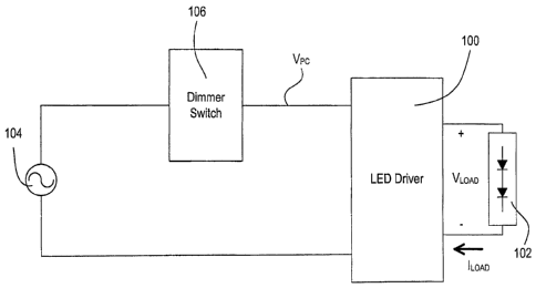
[0049] Fig. 1 is a simplified block diagram of a system including a light-
emitting diode
(LED) driver 100 for controlling the intensity of an LED light source 102
(e.g., an LED light engine)
according to a first embodiment of the present invention. The LED light source
102 is shown as a
plurality of LEDs connected in series but may comprise a single LED or a
plurality of LEDs
connected in parallel or a suitable combination thereof, depending on the
particular lighting system.
In addition, the LED light source 102 may alternatively comprise one or more
organic light-emitting
diodes (OLEDs). The LED driver 100 is coupled to an alternating-current (AC)
power source 104
via a dimmer switch 106. The dimmer switch 106 generates a phase-control
signal Vpc (e.g., a
dimmed-hot voltage), which is provided to the LED driver 100. The dimmer
switch 106 comprises a
bidirectional semiconductor switch (not shown), such as, for example, a triac
or two anti-series-
CA 02776292 2012-03-30
WO 2011/044085
PCT/US2010/051405
- 12 -
connected field-effect transistors (FETs), coupled in series between the AC
power source 104 and
the LED driver 100. The dimmer switch 106 controls the bidirectional
semiconductor switch to be
conductive for a conduction period Tcc=N each half-cycle of the AC power
source 104 to generate the
phase-control signal Vpc.
[0050] The
LED driver 100 is operable to turn the LED light source 102 on and off in
response to the conductive period Tc0N of the phase-control signal Vpc
received from the dimmer
switch 106. In addition, the LED driver 100 is operable to adjust (i.e., dim)
the intensity of the LED
light source 102 to a target intensity LTRGT, which may range across a dimming
range of the LED
light source, i.e., between a low-end intensity LLE (e.g., approximately 1%)
and a high-end
intensity LHE (e.g., approximately 100%) in response to the phase-control
signal Vpc. The LED
driver 100 is able to control both the magnitude of a load current 'LOAD
through the LED light
source 102 and the magnitude of a load voltage VLOAD across the LED light
source. Accordingly,
the LED driver 100 controls at least one of the load voltage VLOAD across the
LED light source 102
and the load current 'LOAD through the LED light source to control the amount
of power delivered to
the LED light source depending upon a mode of operation of the LED driver (as
will be described in
greater detail below).
[0051] The
LED driver 100 is adapted to work with a plurality of different LED light
sources, which may be rated to operate using different load control
techniques, different dimming
techniques, and different magnitudes of load current and voltage. The LED
driver 100 is operable to
control the magnitude of the load current 'LOAD through the LED light source
102 or the load
voltage VLOAD across the LED light source using two different modes of
operation: a current load
control mode (i.e., for using the current load control technique) and a
voltage load control mode (i.e.,
for using the voltage load control technique). The LED driver 100 may also be
configured to adjust
the magnitude to which the LED driver will control the load current 'LOAD
through the LED light
source 102 in the current load control mode, or the magnitude to which the LED
driver will control
the load voltage VLOAD across the LED light source in the voltage load control
mode. When
operating in the current load control mode, the LED driver 100 is operable to
control the intensity of
the LED light source 102 using two different dimming modes: a PWM dimming mode
(i.e., for
using the PWM dimming technique) and a CCR dimming mode (i.e., for using the
CCR dimming
CA 02776292 2012-03-30
WO 2011/044085 PCT/US2010/051405
- 13 -
technique). When operating in the voltage load control mode, the LED driver
100 is only operable
to adjust the amount of power delivered to the LED light source 102 using the
PWM dimming
technique.
[0052] Fig. 2 is a simplified block diagram of the LED driver 100
according to the first
embodiment of the present invention. The LED driver 100 comprises a radio-
frequency (RFI) filter
and rectifier circuit 110, which receives the phase-control signal Vpc from
the dimmer switch 106.
The RFI filter and rectifier circuit 110 operates to minimize the noise
provided on the AC power
source 104 and to generate a rectified voltage VRECT. The LED driver 100
further comprises a power
converter, e.g., a buck-boost flyback converter 120, which receives the
rectified voltage VRECT and
generates a variable direct-current (DC) bus voltage VBus across a bus
capacitor CBus. The flyback
converter 120 may alternatively comprise any suitable power converter circuit
for generating an
appropriate bus voltage. The bus voltage VBus may be characterized by some
voltage ripple as the
bus capacitor CBUS periodically charges and discharges. The flyback converter
120 may also provide
electrical isolation between the AC power source 104 and the LED light source
102, and operate as a
power factor correction (PFC) circuit to adjust the power factor of the LED
driver 100 towards a
power factor of one. Alternatively, the flyback converter 120 could comprise a
boost converter, a
buck converter, a single-ended primary-inductor converter (SEPIC), a uk
converter, or other
suitable power converter circuit.
[0053] The LED driver 100 also comprises an LED drive circuit 130, which
receives the bus
voltage VBuS and controls the amount of power delivered to the LED light
source 102 so as to
control the intensity of the LED light source. The LED drive circuit 130 may
comprise a
controllable-impedance circuit, such as a linear regulator, as will be
described in greater detail
below. Alternatively, the LED drive circuit 130 could comprise a switching
regulator, such as a
buck converter.
[0054] The LED driver 100 further comprises a control circuit 140 for
controlling the
operation of the flyback converter 120 and the LED drive circuit 130. The
control circuit 140 may
comprise, for example, a microcontroller or any other suitable processing
device, such as, for
example, a programmable logic device (PLD), a microprocessor, or an
application specific
integrated circuit (ASIC). The LED driver 100 further comprises a power supply
150, which
CA 02776292 2012-03-30
WO 2011/044085 PCT/US2010/051405
- 14 -
receives the rectified voltage VRECT and generates a plurality of direct-
current (DC) supply voltages
for powering the circuitry of the LED driver. Specifically, the power supply
150 generates a first
non-isolated supply voltage Vcc (e.g., approximately 14 volts) for powering
the control circuitry of
the flyback converter 120, a second isolated supply voltage Vcc2 (e.g.,
approximately 9 volts) for
powering the control circuitry of the LED drive circuit 130, and a third non-
isolated supply
voltage Vcc3 (e.g., approximately 5 volts) for powering the control circuit
140.
[0055] The control circuit 140 is coupled to a phase-control input
circuit 160, which
generates a target intensity control signal VTRGT. The target intensity
control signal VTRGT
comprises, for example, a square-wave signal having a duty cycle DCTRGT, which
is dependent upon
the conduction period Tc0N of the phase-control signal VpG received from the
dimmer switch 106,
and thus is representative of the target intensity LTRGT of the LED light
source 102. Alternatively,
the target intensity control signal VTRGT could comprise a DC voltage having a
magnitude dependent
upon the conduction period TcGN of the phase-control signal Vpc, and thus
representative of the
target intensity LTRGT of the LED light source 102.
[0056] The control circuit 140 is also coupled to a memory 170 for
storing the operational
characteristics of the LED driver 100 (e.g., the load control mode, the
dimming mode, and the
magnitude of the rated load voltage or current). Finally, the LED driver 100
may also comprise a
communication circuit 180, which may be coupled to, for example, a wired
communication link or a
wireless communication link, such as a radio-frequency (RF) communication link
or an infrared (IR)
communication link. The control circuit 140 may be operable to update the
target intensity LTRGT of
the LED light source 102 or the operational characteristics stored in the
memory 170 in response to
digital messages received via the communication circuit 180. For example, the
LED driver 100
could alternatively be operable to receive a full conduction AC waveform
directly from the AC
power source 104 (i.e., not the phase-control signal VpG from the dimmer
switch 106) and could
simply determine the target intensity LTRGT for the LED light source 102 from
the digital messages
received via the communication circuit 180.
[0057] As previously mentioned, the control circuit 140 manages the
operation of the flyback
converter 120 and the LED drive circuit 130 to control the intensity of the
LED light source 102.
The control circuit 140 receives a bus voltage feedback signal VBUS-FB, which
is representative of the
CA 02776292 2012-03-30
WO 2011/044085 PCT/US2010/051405
- 15 -
magnitude of the bus voltage VBUS, from the flyback converter 120. The control
circuit 140 provides
a bus voltage control signal VBUS-CNTL to the flyback converter 120 for
controlling the magnitude of
the bus voltage VBuS (e.g., from approximately 8 volts to 60 volts). When
operating in the current
load control mode, the LED drive circuit 130 controls a peak magnitude Inc of
the load current 'LOAD
conducted through the LED light source 102 between a minimum load current
'LOAD-MIN and a
maximum load current 'LOAD-MAX in response to a peak current control signal
VIM provided by the
control circuit 140. The control circuit 140 receives a load current feedback
signal \Tip:AD, which is
representative of the magnitude of the load current 'LOAD flowing through the
LED light source 102.
The control circuit 140 also receives a LED voltage feedback signal VLED-NEG,
which is
representative of the magnitude of the voltage at the negative terminal of the
LED light source 102.
The control circuit 140 is operable to calculate the magnitude of a load
voltage VLOAD developed
across the LED light source 102 in response to the bus voltage feedback signal
VBUS-FB and the LED
voltage feedback signal VLED-NEG as will be described in greater detail below.
[0058] The control circuit 140 is operable to control the LED drive
circuit 130, so as to
control the amount of power delivered to the LED light source 102 using the
two different modes of
operation (i.e., the current load control mode and the voltage load control
mode). During the current
load control mode, the LED drive circuit 130 regulates the peak magnitude IpK
of the load
current 'LOAD through the LED light source 102 to a target load current ITRGT
in response to the load
current feedback signal VILOAD (i.e., using closed loop control). The target
load current ITRGT may be
stored in the memory 170 and may be programmed to be any specific magnitude
depending upon the
LED light source 102 (as will be described in greater detail below with
reference to Figs. 18-23).
[0059] To control the intensity of the LED light source 102 during the
current load control
mode, the control circuit 140 is operable to control the LED drive circuit 130
to adjust the amount of
power delivered to the LED light source 102 using both of the dimming
techniques (i.e., the PWM
dimming technique and the CCR dimming technique). Using the PWM dimming
technique, the
control circuit 140 controls the peak magnitude IpK of the load current 'LOAD
through the LED light
source 102 to the target load current ITRGT and then pulse-width modulates the
load current 'LOAD to
dim the LED light source 102 to achieve the target load current 'MGT.
Specifically, the LED drive
circuit 130 controls a duty cycle DCBLAD of the load current 'LOAD in response
to a duty cycle DCDim
CA 02776292 2012-03-30
WO 2011/044085 PCT/US2010/051405
- 16 -
of a dimming control signal VDTM provided by the control circuit 140.
Accordingly, the intensity of
the LED light source 102 is dependent upon the duty cycle DCILOAD of the pulse-
width modulated
load current 'LOAD. Using the CCR technique, the control circuit 140 does not
pulse-width modulate
the load current 'LOAD, but instead adjusts the magnitude of the target load
current ITRGT so as to
adjust the DC magnitude of the load current 'LOAD through the LED light source
102.
100601 During the voltage load control mode, the LED drive circuit 130
regulates the DC
voltage of the load voltage VLOAD across the LED light source 102 to a target
load voltage VTRGT.
The target load voltage VTRGT may be stored in the memory 170 and may be
programmed to be any
specific magnitude depending upon the LED light source 102 (as will be
described in greater detail
below with reference to Figs. 18-23). The control circuit 140 is operable to
dim the LED light
source 102 using only the PWM dimming technique during the voltage load
control mode.
Specifically, the control circuit 140 adjusts a duty cycle DCyDDAD of the load
voltage VLOAD to dim
the LED light source 102.
[0061] Fig. 3 is a simplified schematic diagram of the flyback converter
120 and the LED
drive circuit 130. The flyback converter 120 comprises a flyback transformer
210 having a primary
winding coupled in series with a flyback switching transistor, e.g., a field-
effect transistor
(FET) Q212 or other suitable semiconductor switch. The secondary winding of
the flyback
transformer 210 is coupled to the bus capacitor CBuS via a diode D214. The bus
voltage feedback
signal VBUS-FB is generated by a voltage divider comprising two resistors
R216, R218 coupled across
the bus capacitor CBUS. A flyback controller 222 receives the bus voltage
control signal VBUS-CNTL
from the control circuit 140 via a filter circuit 224 and an optocoupler
circuit 226, which provides
electrical isolation between the flyback converter 120 and the control circuit
140. The flyback
controller 222 may comprise, for example, part number TDA4863, manufactured by
Infineon
Technologies. The filter circuit 224 may comprise, for example, a two-stage
resistor-capacitor (RC)
filter, for generating a filtered bus voltage control signal VBUS-CNTL, which
has a DC magnitude
dependent upon a duty cycle DCBus of the bus voltage control signal Vgus-uNTL.
The flyback
controller 222 also receives a control signal representative of the current
through the FET Q212 from
a feedback resistor R228, which is coupled in series with the FET.
CA 02776292 2012-03-30
WO 2011/044085 PCT/US2010/051405
- 17 -
[0062] The flyback controller 222 controls the FET Q212 to selectively
conduct current
through the flyback transformer 210 to thus generate the bus voltage VBus. The
flyback
controller 222 is operable to render the FET Q212 conductive and non-
conductive at a high
frequency (e.g., approximately 150 kHz or less) to thus control the magnitude
of the bus
voltage VBus in response to the DC magnitude of the filtered bus voltage
control signal VBUS-F and
the magnitude of the current through the FET Q212. Specifically, the control
circuit 140 increases
the duty cycle DCBus of the bus voltage control signal VBUS-CNTL, such that
the DC magnitude of the
filter bus voltage control signal Vuus-F increases in order to decrease the
magnitude of the bus
voltage VBus. The control circuit 140 decreases the duty cycle DCBus of the
bus voltage control
signal VBUS-CNTL to increase the magnitude of the bus voltage VBUS.
[0063] As previously mentioned, the LED drive circuit 130 comprises a
linear regulator (i.e.,
a controllable-impedance circuit) including a power semiconductor switch,
e.g., a regulation
field-effect transistor (FET) Q232, coupled in series with the LED light
source 102 for conducting
the load current 'LOAD. The regulation FET Q232 could alternatively comprise a
bipolar junction
transistor (BJT), an insulated-gate bipolar transistor (IGBT), or any suitable
transistor. The peak
current control signal Vim is coupled to the gate of the regulation FET Q232
through a filter
circuit 234, an amplifier circuit 236, and a gate resistor R238. The control
circuit 140 is operable to
control a duty cycle DCB,K of the peak current control signal Vim to control
the magnitude of the
load current 'LOAD conducted through the LED light source 102 to the target
load current ITRGT. The
filter circuit 234 (e.g., a two-stage RC filter) generates a filtered peak
current control signal VIPK-F,
which has a DC magnitude dependent upon the duty cycle DCIpK of the peak
current control
signal Vipx, and is thus representative of the magnitude of the target load
current ITRGT. The
amplifier circuit 236 generates an amplified peak current control signal
VipK_A, which is provided to
the gate of the regulation transistor Q232 through the resistor R238, such
that a gate voltage VIPK-G at
the gate of the regulation transistor Q232 has a magnitude dependent upon the
target load
current ITRGT. The amplifier circuit 236 may comprise a standard non-inverting
operational
amplifier circuit having, for example, a gain a of approximately three.
[0064] A feedback circuit 242 comprising a feedback resistor R244 is
coupled in series with
the regulation FET Q232, such that the voltage generated across the feedback
resistor is
CA 02776292 2012-03-30
WO 2011/044085 PCT/US2010/051405
- 18 -
representative of the magnitude of the load current 'LOAD. For example, the
feedback resistor R244
may have a resistance of approximately 0.0375 Q. The feedback circuit 240
further comprises a
filter circuit 246 (e.g., a two-stage RC filter) coupled between the feedback
resistor R244 and an
amplifier circuit 248 (e.g., a non-inverting operational amplifier circuit
having a gain f3 of
approximately 20). Alternatively, the amplifier circuit 248 could have a
variable gain, which could
be controlled by the control circuit 140 and could range between approximately
1 and 1000. The
amplifier circuit 248 generates the load current feedback signal \Tip:3AD,
which is provided to the
control circuit 140 and is representative of an average magnitude 'AVE of the
load current 'LOAD, e.g.,
'AVE = VILOAD (0 = RFB),
(Equation 1)
wherein RFB is the resistance of the feedback resistor R244. When operating in
the current load
control mode, the control circuit 140 controls the regulation FET Q232 to
operate in the linear
region, such that the magnitude of the load current 'LOAD is dependent upon
the DC magnitude of the
filtered peak current control signal VIPK-F. In other words, the regulation
FET Q232 provides a
controllable-impedance in series with the LED light source 102. When operating
in the voltage load
control mode, the control circuit 140 is operable to drive the regulation FET
Q232 into the saturation
region, such that the magnitude of the load voltage VLOAD is approximately
equal to the magnitude
of the bus voltage VBus (minus the small voltage drops due to the on-state
drain-source
resistance Ros-oN of the FET regulation Q232 and the resistance of the
feedback resistor R244).
[0065] The LED drive circuit 130 also comprises a dimming FET Q250, which
is coupled
between the gate of the regulation FET Q232 and circuit common. The dimming
control signal VDIM
from the control circuit 140 is provided to the gate of the dimming FET Q250.
When the dimming
FET Q250 is rendered conductive, the regulation FET Q232 is rendered non-
conductive, and when
the dimming FET Q250 is rendered non-conductive, the regulation FET Q232 is
rendered
conductive. While using the PWM dimming technique during the current mode of
operation, the
control circuit 140 adjusts the duty cycle DCDim of the dimming control signal
VDBA to thus control
the intensity of the LED light source 102. As the duty cycle DCDE,,I of the
dimming control
signal VDIm increases, the duty cycle DCITRGT, DCvTRGT of the corresponding
load current 'LOAD or
load voltage VLOAD decreases, and vice versa. When using the PWM dimming
technique in both the
current and voltage load control modes, the control circuit 140 is operable to
calculate the peak
magnitude IN( of the load current 'LOAD from the load current feedback signal
VILDAD (which is
CA 02776292 2014-06-20
. ' - 19 -
_
representative of the average magnitude 'AVE of the load current UAL)) and the
duty cycle DCDE,A of
the dimming control signal VD1M, i.e.,
IpK = 'AVE / (1 - DCDim).
(Equation 2)
When using the CCR dimming technique during the current mode of operation, the
control
circuit 140 maintains the duty cycle DCDim of the dimming control signal Vpim
at a high-end
dimming duty cycle DCHE (e.g., approximately 0%, such that the FET Q232 is
always conductive)
and adjusts the target load current ITRGT (via the duty cycle DC wK of the
peak current control
signal VwK) to control the intensity of the LED light source 102.
[0066] The LED voltage feedback signal VLED-NEG is generated by a
voltage divider
comprising two resistors R260, R262 coupled to the negative terminal of the
LED light source 102,
such that the magnitude of the LED voltage feedback signal VLED-NEG is
representative of a regulator
voltage VREG generated across the series combination of the regulation FET
Q232 and the feedback
resistor R244. The control circuit 140 is operable to calculate the magnitude
of a load voltage VLOAD
developed across the LED light source 102 in response to the bus voltage
feedback signal VBUS-FB
and the LED voltage feedback signal VLED-NEG.
[0067] When operating in the current load control mode, the control
circuit 140 is operable
to adjust the magnitude of the bus voltage VBuS to control the magnitude of
the regulator
voltage VREG to a target regulator voltage VREG-TRG1 (i.e., a minimum or "drop-
out" voltage, such as,
for example, approximately two volts). By controlling the regulator voltage
VREG to the target
regulator voltage VREG-TRGT, the control circuit 140 is able to minimize the
magnitude of the
regulator voltage (and thus the power dissipated in the regulation FET Q232)
as well as ensuring that
the regulator voltage does not drop too low and the load voltage VLOAD does
not have any voltage
ripple. Accordingly, the control circuit 140 is operable to optimize the
efficiency and reduce the
total power dissipation of the LED driver 100 by controlling the magnitude of
the bus voltage VBUS,
such that the power dissipation is optimally balanced between the flyback
converter 120 and the
LED drive circuit 130. In other words, the control circuit 140 is operable to
adjust the magnitude of
the bus voltage VBuS in order to reduce the total power dissipation in the
flyback converter 120 and
the LED drive circuit 130. In addition, since the load voltage VLOAD does not
have any voltage
CA 02776292 2014-06-20
- 20
ripple, the peak magnitude IN( of the load current 'TOAD and thus the
intensity of the LED light
source 102 is maintained constant.
[0068] Figs. 4A and 4B are simplified flowcharts of a startup procedure
300 executed by the
control circuit 140 of the LED driver 100 when the control circuit first
starts up at step 310 (e.g.,
when the LED driver 100 is first powered up). If the LED driver 100 is
operating in the current load
control mode (as stored in the memory 170) at step 312, the control circuit
140 determines if the
target load current ITRGT and the dimming method are known (i.e., are stored
in the memory 170) at
steps 314, 316. If the target load current ITRG1 and the dimming method are
known at steps 314, 316,
and the dimming method is the PWM dimming technique at step 318, the control
circuit 140 sets the
duty cycle DCnim of the dimming control signal ViDim equal to a low-end
dimming duty cycle DCLI
at step 320. For example, the low-end duty cycle DCLE may be approximately
99%, such that the
dimming FET Q250 is rendered conductive 99% of the time, thus causing the
regulation FET Q232
to be rendered conductive approximately 1% of the time (i.e., to control the
intensity of the LED
light source 102 to the low-end intensity LLE). If the dimming method is the
CCR dimming
technique at step 318, the control circuit 140 sets the duty cycle DC[ilm of
the dimming control
signal ViDim equal to the high-end dimming duty cycle DCHE (i.e.,
approximately 0%) at step 322.
The control circuit 140 then sets the duty cycle DCIpK of the peak current
control signal Vim to a
minimum peak current duty cycle DCmIN at step 324.
[0069] Next, the control circuit 140 executes a current load control
procedure 500 (which
will be described in greater detail below with reference to Fig. 6) in order
to regulate the peak
magnitude IpK of the load current 'LOAD flowing through the feedback resistor
R244 to the target load
current ITRGT and to regulate the regulator voltage VREG across the series
combination of the
regulation FET Q232 and the feedback resistor R244 to the target regulator
voltage VREG-TRGT. The
control circuit 140 may calculate the peak magnitude Ipi{ of the load current
'TOAD from t he
magnitude of the load current feedback signal V1LOAD using equations 1 and 2
shown above. If the
peak magnitude IN( of the load current 'LOAD is not equal to the target load
current IfRGT at step 326,
or if the regulator voltage VREG (as determined from the LED voltage feedback
signal VLED-NEG) is
not equal to the target regulator voltage VREG-TRGT at step 328, the control
circuit 140 executes the
current load control procedure 500 once again. The control circuit 140
continues to execute the
CA 02776292 2012-03-30
WO 2011/044085 PCT/US2010/051405
-21 -
current load control procedure 500 until the load current 'LOAD is equal to
the target load
current ITRGT at step 326 and the regulator voltage VREG is equal to the
target regulator
voltage VREG-TRGT at step 328.
[0070] When the peak magnitude IN( of the load current 'LOAD is equal to
the target load
current ITRGT at step 326 and the regulator voltage VREG is equal to the
target regulator
voltage VREG-TRGT at step 328, the control circuit 140 determines if the
dimming method is the PWM
dimming technique at step 330. If not, the startup procedure 300 simply exits.
However, if the
dimming method is the PWM dimming technique at step 330, the control circuit
140 sets the duty
cycle DCDEvi of the dimming control signal Vpim equal to a target dimming duty
cycle DCTRGT at
step 332 to control the intensity of the LED light source 102 to the target
intensity LTRGT and the
startup procedure 300 exits.
[0071] If the target load current ITRGT or the dimming method is not
known (i.e., is not stored
in the memory 170) at steps 314, 316, the control circuit 140 changes to the
CCR dimming mode at
step 334 and sets the duty cycle DCDEA of the dimming control signal ViDim
equal to the high-end
dimming duty cycle DC HE and the target load current ITRG equal to the minimum
load
current 'LOAD-MIN (e.g., approximately two milliamps) at step 336. The control
circuit 140 then
regulates the load current 'LOAD to be equal to the minimum load current 'LOAD-
MIN using the current
load control procedure 500, before the startup procedure 300 exits. If the LED
driver 100 is
operating in the voltage load control mode at step 312 and the target load
voltage VTRGT is not
known (i.e., not stored in the memory 170) at step 338, the control circuit
140 changes to the current
load control mode at step 340. The control circuit 140 then changes to the CCR
dimming mode at
step 334 and sets the duty cycle DCDim of the dimming control signal VElim to
the high-end dimming
duty cycle DCHE and the target load current ITRGT to the minimum load current
'LOAD-MIN at step 336,
before the control circuit 140 regulates the load current 'LOAD to the minimum
load current ILOAD-miN
using the current load control procedure 500 and the startup procedure 300
exits. Because at least
one of the target load current ITRGT and the dimming method is not known, the
control circuit 140
controls the flyback converter 120 and the LED drive circuit 130 to provide
the minimum amount of
current to the LED light source 102 such that the LED light source is not
damaged by being exposed
to excessive voltage or current.
CA 02776292 2012-03-30
WO 2011/044085 PCT/US2010/051405
- 22 -
[0072] Referring to Fig. 4B, if the LED driver 100 is operating in the
voltage load control
mode at step 312 and the target load voltage VTRGT is known (i.e., stored in
the memory 170) at
step 338, the control circuit 140 determines a current limit 'Limn to which
the load current 'LOAD will
be limited during the voltage load control mode. Specifically, if a maximum
power dissipation PmAx
divided by the target load voltage VTRGT is less than a maximum load current
ImAx at step 342, the
control circuit 140 sets the current limit 'Lima to be equal to the maximum
power dissipation PmAx
divided by the target load voltage VTRGT at step 344. Otherwise, the control
circuit 140 sets the
current limit Iumn to be equal to the maximum load current ImAx at step 346.
At step 348, the
control circuit 140 sets the duty cycle DCR)K of the peak current control
signal Vim to a maximum
peak current duty cycle DC mAx (i.e., 100%). At step 350, the control circuit
140 sets the duty
cycle DCDim of the dimming control signal Vpim equal to the low-end dimming
duty cycle DCLE,
such that the dimming FET Q250 is rendered conductive 99% of the time, and the
regulation
FET Q232 is rendered conductive approximately 1% of the time.
[0073] Next, the control circuit 140 regulates the load voltage VLOAD
across the LED light
source 102 to the target load voltage VTRGT using a voltage load control
procedure 600 (which will
be described in greater detail below with reference to Fig. 7). If the load
voltage VLOAD is not equal
to the target load voltage VTRGT at step 352, the control circuit 140 executes
the voltage load control
procedure 600 once again. When the load voltage VLOAD is equal to the target
load voltage VTRGT at
step 352, the control circuit 140 sets the duty cycle DCDE,A of the dimming
control signal VDIm equal
to the target dimming duty cycle DCTRGT at step 354 to control the intensity
of the LED light
source 102 to the target intensity LTRGT and the startup procedure 300 exits.
[0074] Fig. 5 is a simplified flowchart of a target intensity procedure
400 executed by the
control circuit 140 of the LED driver 100 (when both the target load current
ITRGT or the dimming
method are known). The eontrol circuit 140 executes the target intensity
procedure 400 when the
target intensity LTRGT changes at step 410, for example, in response to a
change in the DC magnitude
of the target intensity control signal VTRGT generated by the phase-control
input circuit 160. If the
LED driver 100 is operating in the current load control mode (as stored in the
memory 170) at
step 412, the control circuit 140 determines at step 414 if the LED driver is
using the PWM dimming
technique (as stored in the memory 170). If so, the control circuit 140
adjusts the duty cycle DCEqm
CA 02776292 2014-06-20
= - 23
of the dimming control signal Vpim at step 416 in response to the new target
intensity LTRGT, so as to
control the intensity of the LED light source 102 to the new target intensity
LTRGT. If the LED
driver 100 is operating in the current load control mode at step 412 and with
the CCR dimming
technique at step 414, the control circuit 140 adjusts the target load current
ITRGT of the load
current 'LOAD in response to the new target intensity LTRGT at step 418 before
the target intensity
procedure 400 exits. Specifically, the control circuit 140 adjusts the duty
cycle DCIpic of the peak
current control signal V1131( at step 418, so as to control the magnitude of
the load current 'LOAD
towards the target load current ITRGT. If the LED driver 100 is operating in
the voltage load control
mode at step 412, the control circuit 140 adjusts the duty cycle DCDim of the
dimming control
signal VDEvi in response to the new target intensity LTRGT at step 416 and the
target intensity
procedure 400 exits.
[0075]
Fig. 6 is a simplified flowchart of the current load control mode
procedure 500, which
is executed periodically by the control circuit 140 when the LED driver 100 is
operating in the
current load control mode. The current load control mode procedure 500 allows
the control
circuit 140 to regulate the peak magnitude Im of the load current 'LOAD
flowing through the feedback
resistor R244 to the target load current ITRGT and to control the magnitude of
the regulator
voltage VREG across the series combination of the regulation FET Q232 and the
feedback
resistor R244 by controlling the magnitude of the bus voltage VBus. For
example, the control
circuit 140 may determine the peak magnitude of the load current 'LOAD from
the average
magnitude 'AVE of the load current 'LOAD and the duty cycle DCDim of the
dimming control
signal Vijim , i.e., Ipi( = 'AVE / (1 - DCoim), as shown in Equation 2 above.
If the peak magnitude Ipk
of the load current 'LOAD is less than the target load current ITRG1 at step
510, the control circuit 140
increases the duty cycle DCipic of the peak current control signal Vim( by a
predetermined
percentage ADCIpK at step 512. Accordingly, the magnitude of the gate voltage
VipK_G at the gate of
the regulation FET Q232 will increase, thus causing the peak magnitude 'pi( of
the load current 'LOAD
to increase. If the load current 'LOAD is not less than the target load
current ITRGT at step 510, but is
greater than the target load current ITRGT at step 514, the control circuit
140 decreases the duty
cycle DCim of the peak current control signal Vim{ by the predetermined
percentage ADCwK at
step 516 to decrease the peak magnitude Ipi( of the load current 'LOAD.
CA 02776292 2012-03-30
WO 2011/044085 PCT/US2010/051405
- 24 -
[0076] Next, the control circuit 140 adjusts the magnitude of the bus
voltage VBUS in order to
minimize the regulator voltage VREG to minimize the power dissipation in the
FET Q232, while
ensuring that the regulator voltage does not drop too low and the load voltage
VLOAD does not have
any voltage ripple. Specifically, if the regulator voltage VREG (as determined
from the LED voltage
feedback signal VLED-NEG) is greater than the target regulator voltage VREG-
TRGT at step 518, the
control circuit 140 increases the duty cycle DCBus of the bus voltage control
signal VBus-ci\ITL by the
predetermined percentage ADCBus at step 520 to decrease the magnitude of the
bus voltage VBUS
and thus decrease the magnitude of the regulator voltage VREG. If the
regulator voltage VREG is not
greater than the target regulator voltage VREG-TRGT at step 518, but is less
than the target regulator
voltage VREG-TRGT at step 522, the control circuit 140 decreases the duty
cycle DCBus of the bus
voltage control signal VBuS-CNTL by the predetermined percentage ADCBus at
step 524 to increase the
magnitude of the bus voltage VBUS to ensure that the regulator voltage VREG
does not drop too low.
If the load current 'LOAD is equal to the target load current ITRGT at steps
510, 514, and the regulator
voltage VREG is equal to the target regulator voltage VREG_TRGT at steps 518,
522, the current load
control mode procedure 500 simply exits without adjusting the duty cycle
DCipic of the peak current
control signal Vim{ or the duty cycle DCBus of the bus voltage control signal
VBus-cNTL.
[0077] Fig. 7 is a simplified flowchart of a voltage load control mode
procedure 600, which
is executed periodically by the control circuit 140 when the LED driver 100 is
operating in the
voltage load control mode. The voltage load control mode procedure 600 allows
the control
circuit 140 to regulate the load voltage VLOAD to the target load voltage
VTRGT by controlling the
magnitude of the bus voltage VBUS. If the magnitude of the load current 'LOAD
is less than the current
limit Iumrr at step 610, the control circuit 140 subtracts the magnitude of
the regulator voltage VREG
(as represented by the LED voltage feedback signal VLED-NEG) from the
magnitude of the bus
voltage VBUS (as represented by the bus voltage feedback signal VBus-FB) at
step 612 to calculate the
magnitude of the load voltage VLOAD. If the load voltage VLOAD is less than
the target load
voltage VTRGT at step 614, the control circuit 140 decreases the duty cycle
DCBus of the bus voltage
control signal VBUS-CNTL using a proportional-integral-derivative (PID)
control technique at step 616
to thus increase the magnitude of the bus voltage VBUS, before the voltage
load control mode
procedure 600 exits. If the load voltage VLOAD is not less than the target
load voltage VTRGT at
step 614, but is greater than the target load voltage VTRGT at step 618, the
control circuit 140
CA 02776292 2014-06-20
= - 25 -
increases the duty cycle DCBus of the bus voltage control signal VBUS-CNTL
using the PID control
technique at step 620 to thus decrease the magnitude of the bus voltage VBUS,
before the voltage load
control mode procedure 600 exits. If the load voltage VLOAD is not less than
the target load
voltage VTRGT at step 614 and is not greater than the target load voltage V
rRoT at step 618 (i.e.,
the load voltage VLoAD is equal to the target load voltage V FRGT), the
voltage load control mode
procedure 600 exits without adjusting the duty cycle DCBus of the bus voltage
control
signal VBUS-CNTL=
[0078] If the magnitude of the load current 'LOAD is greater than or
equal to the current
limit ILINHT at step 610, the control circuit 140 begins to operate in an
overcurrent protection mode at
step 622 in order to limit the load current 'LOAD to be less than the current
limit 'LIMIT. For example,
the control circuit 140 may decrease the duty cycle DCipi( of the peak current
control signal Vim
until the load current 'LOAD becomes less than the current limit 'LIMIT at
step 624. During the
overcurrent protection mode, the load voltage VLOAD may drop lower than the
target load
voltage VTRG r. The control circuit continues to operate in the overcurrent
protection mode at
step 622 while the magnitude of the load current 'LOAD remains greater than or
equal to the current
limit Limn- at step 624. When the magnitude of the load current 'LOAD
decreases below the current
limit luvirr at step 624, the control circuit 140 executes the startup
procedure 300 (as shown in
Figs. 4A and 4B) and the voltage load control mode procedure 600 exits.
[0079] Fig. 8 is a simplified schematic diagram of an LED drive
circuit 730 of an LED
driver 700 according to a second embodiment of the present invention. The LED
drive circuit 730 is
controlled by a control circuit 740 in response to the peak current control
signal Vim in a similar
manner as the control circuit 140 controls the LED drive circuit 130 of the
first embodiment. In the
current load control mode, the control circuit 740 is operable to control the
peak magnitude Ipic of
the load current 'LOAD to range from approximately the minimum load current
'LOAD-MIN to the
maximum load current 'LOAD-MAX to dim the LED light source 102 across the
dimming range.
According to the second embodiment of the present invention, the maximum load
current 'LOAD-MAX
is at least one hundred times greater than the minimum load current 'LOAD-MIN.
For example, the
minimum load current 'LOAD-MIN may be approximately two milliamps, and the
maximum load
CA 02776292 2014-06-20
= - 26
current 'LOAD-MAX may be approximately two amps, such that the maximum load
current 'LOAD-MAX is
one thousand times greater than the minimum load current 'LOAD-MIN
[0080] The LED drive circuit 730 comprises a regulation FET Q732
coupled in series with
the LED light source 102 for controlling the magnitude of the load current
LOAD conducted through
the LED light source 102. The LED drive circuit 730 comprises a filter circuit
734 that receives the
peak current control signal Vim from the control circuit 740 and generates the
filtered peak current
control signal VipK-F. Specifically, the filter circuit 734 comprises a two-
stage RC filter having two
resistors R738A, R738B (e.g., both having resistances of approximately 10 kiI)
and two
capacitors C739A, C7398 (e.g., both having capacitances of approximately 1
pf). As shown in
Fig. 8, the filter circuit 734 is referenced to the source of the regulation
FET Q732. The filtered peak
current control signal Vipx-F is coupled to the gate of the regulation FET
Q732 via an amplifier
circuit 736 and a resistor R735 (e.g., having a resistance of approximately
150 Q). The amplifier
circuit 736 may have, for example, a gain x of approximately one, such that
the amplifier circuit
simply operates as a buffer.
[0081] The LED drive circuit 730 also comprises a dimming FET Q750,
which is controlled
in response to the dimming control signal Vpim from the control circuit 140 to
dim the LED light
source 102 using the PWM dimming technique (in a similar manner as the dimming
FET Q250 of
the first embodiment is controlled). An NPN bipolar junction transistor Q752
is coupled between
the filter circuit 734 and the amplifier circuit 736 for selectively coupling
the filtered peak current
control signal VIPK-F to the amplifier circuit. The dimming FET Q750 is
coupled to the base of the
transistor Q752 via a resistor R754 (e.g., having a resistance of
approximately 1001(0). A
resistor R756 is coupled between the emitter and the base of the transistor
Q752 and has, for
example, a resistance of approximately 100 Ica When the dimming FET Q750 is
controlled to be
conductive, the transistor Q752 is also rendered conductive, thus coupling the
filtered peak current
control signal VIPK-F to the amplifier circuit 736, such that the regulation
FET Q732 is controlled to
be conductive. When the dimming FET Q750 is controlled to be non-conductive,
the
transistor Q752 is also rendered non-conductive and the filtered peak current
control signal VIPK-F is
not provided to the amplifier circuit 736, such that the regulation FET Q732
is rendered
non-conductive.
CA 02776292 2012-03-30
WO 2011/044085 PCT/US2010/051405
- 27 -
[0082] The LED drive circuit 730 comprises a current mirror circuit R760,
which is coupled
across the LED light source 102 and generates a load voltage feedback signal
VLOAD-FB
representative of the magnitude of the load voltage VLOAD- The control circuit
740 receives the load
voltage feedback signal VLOAD-FB, such that the control circuit does not need
to calculate the
magnitude of the load voltage by subtracting the magnitude of the regulator
voltage VREG from the
magnitude of the bus voltage VBUS (as in the first embodiment). The load
voltage feedback
signal VLOAD-FB is also provided to an inverting input of a comparator 762 for
providing over-voltage
protection for the LED drive circuit 730. When the magnitude of the load
voltage feedback
signal VLOAD-FB exceeds the magnitude of a first reference voltage VREF1, the
comparator 762 is
operable to pull the gate of the regulation FET Q732 down towards circuit
common, thus rendering
the regulation FET Q732 non-conductive and controlling the load voltage VLOAD
to approximately
zero volts. The magnitude of the first reference voltage VREF1 corresponds to
a magnitude of the
load voltage VLOAD that represents an over-voltage condition for the LED light
source 102. For
example, the magnitude of the first reference voltage VREF1 may be chosen such
that the regulation
FET Q732 is rendered non-conductive when the magnitude of the load voltage
VLOAD exceeds
approximately 40 volts for a Class 2 LED light source.
[0083] The LED drive circuit 730 comprises an adjustable gain feedback
circuit 770 that
allows the control circuit 740 to properly measure the peak magnitude IpK of
the load current 'LOAD
from the minimum load current 'LOAD-MIN to the maximum load current 'LOAD-MAX,
which may be
approximately one thousand times greater than the minimum load current 'LOAD-
MIN- The adjustable
gain feedback circuit 770 comprises a filter circuit 746 and an amplifier
circuit 748 for generating
the load current feedback signal VILOAD (in a similar manner as the filter
circuit 246 and the
amplifier circuit 248 of the feedback circuit 242 of the first embodiment).
The amplifier circuit 748
may comprise a non-inverting operational amplifier circuit having a gain y
(e.g., approximately 20).
The adjustable gain feedback circuit 770 is controlled to adjust the magnitude
of the load current
feedback signal ViLoAD in response to a gain control signal VGAIN generated by
the control
circuit 740 when operating in the current load control mode. The adjustable
gain feedback
circuit 770 comprises two feedback resistors R772, R774, which are coupled in
series with the
regulation FET Q732 (i.e., to replace the feedback resistor R244 of the
feedback circuit 242 of the
first embodiment). For example, the resistors R772, R774 may have resistances
of approximately
CA 02776292 2012-03-30
WO 2011/044085 PCT/US2010/051405
- 28 -
0.0375 C2 and 1.96 f2, respectively. A FET Q775 is coupled across the second
feedback
resistor R774 and is controlled to be conductive and non-conductive to control
the gain (i.e., the
magnitude) of the load current feedback signal VIL0AD. The gain control signal
VGAIN is coupled to
the gate of the FET Q775 via a drive circuit comprising a FET Q776 and two
resistors R778, R779
(e.g., having resistances of approximately 5 kì and 1 kt2, respectively).
[0084] According to the second embodiment of the present invention, the
gain control
signal VGAIN is controlled so as to adjust the equivalent resistance RFB of
the adjustable gain
feedback circuit 770 (to thus increase the gain of the adjustable gain
feedback circuit) when the
magnitude of the load current 'LOAD is less than or equal to a threshold
current ITH (e.g.,
approximately 100 mA). The magnitude of the load current 'LOAD crosses the
threshold current ITH
in the middle of the dimming range of the LED driver 700. When the magnitude
of the load
current 'LOAD is less than or equal to the threshold current ITH, the gain
control signal VGAIN is
controlled to be high (i.e., at approximately the third supply voltage Vcc3),
such that the FET Q776
is rendered conductive and the gate of the FET Q775 is pulled down towards
circuit common.
Accordingly, the FET Q775 is rendered non-conductive, and both the first and
second feedback
resistors R772, R774 (i.e., approximately 2 S2 total resistance) is coupled in
series with the regulation
FET Q732. When the magnitude of the load current 'LOAD is greater than the
threshold current ITH,
the gain control signal VGAIN is controlled to be low (i.e., at approximately
circuit common)
rendering the FET Q776 non-conductive, such that the gate of the FET Q775 is
pulled up towards
the second supply voltage VCC2, and the FET Q775 is rendered conductive. Thus,
only the first
feedback resistor R772 (i.e., approximately 0.0375 S2) is coupled in series
with the regulation
FET Q732. For example, the control circuit 740 may control the gain control
signal VGAIN using
some hysteresis, such that the FET Q775 is not quickly and unstably rendered
conductive and
non-conductive.
[0085] When the FET Q775 of the adjustable gain feedback circuit 770 is
rendered
conductive and non-conductive, there is a step change in the resistance
coupled in series with the
regulation FET Q732 (and thus a step change in the magnitude of the voltage at
the source of the
regulation FET). As a result, there may also be a sharp change in the load
current 'LOAD, which
could cause a slight and temporary increase or decrease (e.g., a "blip") in
the intensity of the LED
CA 02776292 2014-06-20
= - 29 -
light source 102. Because the threshold current ITH is in the middle of the
dimming range of the
LED driver 100, it is very desirable to have no fluctuations of the intensity
of the LED light
source 102 as the intensity of the LED light source is being dimmed up or
dimmed down. Since the
filter circuit 734 is referenced to the source of the regulation FET Q732,
changes in the magnitude of
the voltage at the source do not greatly affect the magnitude of the peak
current control signal VIPK
and thus the gate-source voltage of the regulation FET Q732. Accordingly, the
large fluctuations of
the load current 'LOAD (and thus the intensity of the LED light source 102)
are minimized when the
FET Q775 is rendered conductive and non-conductive at the threshold current
'TH.
[0086] In addition, the control circuit 740 "pre-loads" the peak
current control signal Vim<
whenever the magnitude of the load current 'LOAD transitions above or below
the threshold
current ITH to avoid large fluctuations of the load current 'LOAD and thus the
intensity of the LED
light source 102. Specifically, when the magnitude of the load current 'LOAD
transitions across the
threshold current ITH, the control circuit 740 enters a transition mode in
which the closed loop
control of the regulation FET Q732 (i.e., the current load control procedure
500) is paused. After
entering the transition mode, the control circuit 740 adjusts the peak current
control signal Vim{ by a
predetermined correction factor AVipK, and then waits for a first delay time
TDELAY1 (e.g.,
approximately one to two milliseconds) before controlling the gain control
signal VGAIN to render the
FET Q775 either conductive or non-conductive. After controlling the FET Q775,
the control
circuit 740 waits for a second delay time TDELAY2 after which the control
circuit exits the transition
mode and resumes the close loop control of the regulation FET Q732. For
example, the second
delay time TDELAY2 may be approximately ten milliseconds when the magnitude of
the load
current 'LOAD has transitioned above the threshold current ITH and
approximately four milliseconds
when the magnitude of the load current 'LOAD has transitioned below the
threshold current 1m.
[0087] Referring back to Fig. 8, the LED drive circuit 730 further
comprises an over-current
protection circuit having an amplifier circuit 764 (e.g., having a gain z of
approximately two) and a
comparator 766. When the magnitude of load current UAL) increases such that
the magnitude of the
voltage at the non-inverting input of the comparator 766 exceeds the magnitude
of a second
reference voltage VREF2, the comparator 766 is operable to pull the gate of
the regulation FET Q732
down towards circuit common, thus rendering the regulation FET Q732 non-
conductive and
CA 02776292 2012-03-30
WO 2011/044085 PCT/US2010/051405
- 30 -
controlling the load current 'LOAD to approximately zero amps. The magnitude
of the second
reference voltage VREF2 corresponds to a magnitude of the load current 'LOAD
that represents an
over-current condition through the LED light source 102. For example, the
magnitude of the second
reference voltage VREF2 may be chosen such that the regulation FET Q732 is
rendered
non-conductive when the magnitude of the load current 'LOAD exceeds
approximately four amps.
[0088] Fig. 9 is a simplified flowchart of a transition mode procedure
800 executed
periodically by the control circuit 740 when the LED driver 700 is operating
in the current load
control mode. During the transition mode procedure 800, the control circuit
740 begins operating in
a transition mode if the magnitude of the load current 'LOAD has just
transitioned across the threshold
current ITH. If the control circuit 740 is not in the transition mode at step
810 when the transition
mode procedure 800 begins, the control circuit first executes the current load
control procedure 500
(as shown in Fig. 6). For example, the control circuit 740 may calculate the
peak magnitude IN( of
the load current 'LOAD using Equations 1 and 2 shown above, where the
equivalent resistance RFB of
the adjustable-gain feedback circuit 770 is dependent upon the state of the
FET Q775. For example,
the equivalent resistance RFB may be equal to approximately the resistance of
the resistor R772
when the FET Q775 is conductive, and may be equal to approximately the
resistance of the series
combination of the first and second feedback resistors R772, R774 when the FET
Q775 is
non-conductive.
[0089] After executing the current load control mode procedure 500, the
control circuit 740
then checks to determine if the magnitude of the load current 'LOAD just
transitioned across the
threshold current ITH. Specifically, if the magnitude of the load current
'LOAD has risen above the
threshold current ITH at step 812, the control circuit 740 adds the correction
factor AVII,K to the peak
current control signal Vim( at step 814 and enters the transition mode at step
816 (i.e., execution of
the current load control procedure 500 is paused). The control circuit 740
then initializes a first
delay timer to the first delay time TDELAY1 and starts the first delay timer
decreasing in value with
respect to time at step 818, before the transition mode procedure 800 exits.
If the magnitude of the
load current 'LOAD has just dropped below the threshold current ITH at step
820, the control
circuit 740 subtracts the correction factor AVH)K from the peak current
control signal Vim at
CA 02776292 2014-06-20
_ = - 31 -
step 822, enters the transition mode at step 816, and starts the first delay
timer with the first delay
time TDELAY1 at step 818, before the transition mode procedure 800 exits.
[00901 When the control circuit 740 is in the transition mode at
step 810, the control
circuit 740 does not execute the current load control procedure 500, and
rather operates to control
the FET Q775 to adjust the gain of the adjustable-gain feedback circuit 770.
Specifically, when the
first delay timer expires at step 824 and the magnitude of the load current
'LOAD has risen above the
threshold current ITH at step 826, the control circuit 740 drives the gain
control signal VGAIN low at
step 828 to render the FET Q775 conductive, such that only the first feedback
resistor R772 is
coupled in series with the regulation FET Q732. The control circuit 740 then
updates the equivalent
resistance RFB of the adjustable gain feedback circuit 770 to be equal to the
resistance of only the
resistor R772 at step 830. At step 832, the control circuit 740 initializes a
second delay timer to the
second delay time TDELAy2 and starts the second delay timer decreasing in
value with respect to time,
before the transition mode procedure 800 exits.
[0091] When the first delay timer expires at step 824 and the
magnitude of the load
current 'LOAD has dropped below the threshold current ITH at step 826, the
control circuit 740 drives
the gain control signal VG/km high at step 834 to render the FET Q775 non-
conductive, such that
both the first and second feedback resistors R772, R774 are coupled in series
with the regulation
FET Q732. The control circuit 740 then adjusts resistance RFB of the
adjustable gain feedback
circuit 770 to be equal to the resistance of the series combination of the
resistors R772, R774 at
step 830, and starts the second delay timer with the second delay time TDELAY2
at step 832, before the
transition mode procedure 800 exits. When the second delay timer expires at
step 836, the control
circuit 740 exits the transition mode at step 838, such that when the
transition mode procedure 800 is
executed again, the current load control procedure 500 will be executed.
[0092] Fig. 10 is a simplified block diagram of an LED driver 900
according to a third
embodiment of the present invention. The LED driver 900 of the third
embodiment includes many
similar functional blocks as the LED driver 100 of the first embodiment as
shown in Fig. 2.
However, the LED driver 900 of the third embodiment does not include the power
supply 150.
Rather, the LED driver 900 comprises a buck-boost flyback converter 920, which
generates the
CA 02776292 2014-06-20
- 32
variable DC bus voltage VBus across the bus capacitor CBus, as well as
generating the various DC
supply voltages Vcci, VCC2, VCC3 for powering the circuitry of the LED driver.
[0093] In addition, the LED drive circuit 930 includes a multiple-output
feedback circuit 970
(Fig. 12) that provides first and second load current feedback signals
VILOADI, VILOAD2 to a control
circuit 940. The first load current feedback signal VILOAD1 is characterized
by a first gain yi applied
to the average magnitude 'AVE of the load current 'LOAD, while the second load
current feedback
signal VILOAD2 is characterized by a second gain 72. The second gain 72 (e.g.,
approximately 101) is
greater than the first gain 71 (e.g., approximately one), such that the first
and second load current
feedback signals VILOADI, VILOAD2 provide two differently scaled
representations of the average
magnitude 'AVE of the load current 'LOAD. The control circuit 940 uses both of
the first and second
load current feedback signals VILOADI, VILOAD2 to determine the peak magnitude
III( of the load
current 'LOAD, which may range from the minimum load current 'LOAD-MIN to the
maximum load
current 'LOAD-MAX (as will be described in greater detail below). Accordingly,
the maximum load
current 'LOAD-MAX may be at least one hundred times greater than the minimum
load
current 'LOAD-MIN, for example, approximately one thousand times greater than
the minimum load
current 'LOAD-MIN, as in the second embodiment.
[0094] Fig. 11 is a simplified circuit diagram of the flyback converter
920 of the LED
driver 900 of the third embodiment of the present invention. The flyback
converter 920 comprises a
flyback transformer 910 having a primary winding coupled in series with a FET
Q912 and a
feedback resistor R926. The secondary winding of the flyback transformer 910
is coupled to the bus
capacitor CBus via a diode D914. The secondary winding of the flyback
transformer 910 comprises
a center tap that generates a center tap voltage V Ap having a magnitude
proportional to the
magnitude of the bus voltage VBus. The bus voltage feedback signal VBUS-FB is
generated by a
voltage divider comprising two resistors R916, R918 coupled across the bus
capacitor CBUS and is
provided to the control circuit 940. The center tap voltage V FAB is used to
generate the second
supply voltage VCC2 and the third supply voltage Vcc3 as will be described in
greater detail below.
[0095] The flyback converter 920 comprises a flyback controller 922,
which operates in a
similar manner as the flyback controller 222 of the flyback converter 120 of
the first embodiment to
generate the bus voltage VBus across the bus capacitor CBus. The flyback
controller 922 controls the
CA 02776292 2014-06-20
- 33 -
FET Q912 in response to the bus voltage control signal VBus_uNTL received from
the control
circuit 940 (via a filter circuit 924 and an optocoupler circuit 926) and a
control signal received from
the feedback resistor R928 and representative of the current through the FET
Q912.
[0096] The flyback converter 920 comprises a flyback controller power
supply 932 for
generating the first DC supply voltage Vcc (e.g., approximately 14 volts for
powering the flyback
controller 922) across a capacitor C929 (e.g., having a capacitance of
approximately 220 F). The
flyback controller power supply 932 is coupled to a supply winding 910A of the
flyback transformer
910, such that the flyback controller power supply is only able to generate
the first DC supply
voltage Vcc1 while the flyback converter 920 is actively generating the DC bus
voltage VBus (i.e.,
after the flyback controller 922 has started up). The flyback controller power
supply 932 comprises
a pass-transistor supply that includes an NPN bipolar junction transistor
Q934, a resistor R935 (e.g.,
having a resistance of approximately 10 1(0), a zener diode Z936 (e.g., having
a breakover voltage of
approximately 14 volts), and a diode D938. The emitter of the transistor Q934
is coupled to the
capacitor C929 through the diode D938 and the zener diode Z936 is coupled to
the base of the
transistor Q934. Accordingly, the capacitor C929 is able to charge through the
transistor Q934 to a
voltage equal to approximately the break-over voltage of the zener diode Z936
minus the
base-emitter drop of the transistor and the diode drop of the diode D938.
[0097] Since the flyback controller power supply 932 is only able to
generate the first DC
supply voltage Vcci while the flyback converter 920 is actively generating the
DC bus voltage VBUS,
the flyback converter further comprises a startup power supply 950 for
allowing the capacitor C929
to charge before the flyback controller 922 has started up. The startup power
supply 950 comprises
a cat-ear power supply including a FET Q952 for allowing the capacitor C929 to
charge from the
rectified voltage VREcT through a diode D954 and a resistor R956 (e.g., having
a resistance of
approximately 1 Q). The gate of the FET Q952 is coupled to the rectified
voltage VRECT through
two resistors R958, R960 (e.g., having resistances of approximately 250 IcQ
and 200 kQ,
respectively), such that shortly after the beginning of a half-cycle of the AC
power source 104, the
FET 952 is rendered conductive allowing the capacitor C929 to charge. An NPN
bipolar junction
transistor Q962 is coupled to the gate of the FET Q952 for providing over-
current protection in the
startup power supply 950. Specifically, if the current through the FET Q952
increases such that the
CA 02776292 2012-03-30
WO 2011/044085 PCT/US2010/051405
- 34 -
voltage across the resistor R956 exceeds the rated base-emitter voltage of the
transistor Q962, the
transistor Q962 becomes conductive, thus rendering the FET 952 non-conductive.
[0098] The gate of the FET Q952 is coupled to circuit common via an NPN
bipolar junction
transistor Q964. The base of the transistor Q964 is coupled to the rectified
voltage VRECT via the
resistor R958, a zener diode Z965 (e.g., having a breakover voltage of
approximately 5.6 volts), and
another resistor R966 (e.g., having a resistance of approximately 1 MU). A
resistor R968 is coupled
between the base and the emitter of the transistor Q964 and has, for example,
a resistance of
approximately 392 ka When the magnitude of the rectified voltage VRECT
increases to a magnitude
such that the voltage across the resistor R968 exceeds the breakover voltage
of the zener diode Z965
and the base-emitter voltage of the transistor Q964, the transistor Q964 is
rendered conductive, thus
pulling the gate of the FET 952 down towards circuit common. Accordingly, the
FET 952 is
rendered non-conductive preventing the capacitor C929 from charging from the
rectified
voltage VRECT. As a result, the startup power supply 950 only allows the
capacitor C929 to charge
around the zero-crossings of the AC power source 104, and thus provide more
efficient operation
during startup of the flyback controller 922 than, for example, simply having
a single resistor
coupled between the rectified voltage VRECT and the capacitor C929. After the
capacitor C929 has
appropriately charged (i.e., the magnitude of the first DC supply voltage Vcci
has exceeded the rated
operating voltage of the flyback controller 922), the flyback controller power
supply 932 is able to
generate the first DC supply voltage Vcci and the startup power supply 950
ceases operating.
However, the startup power supply 950 may once again begin operating during
normal operation if
the voltage across the supply winding 910A drops below approximately the first
DC supply
voltage Vcc t=
[0099] The flyback converter 920 further comprises first and second power
supplies 980, 990
that have outputs that are coupled together. The first and second power
supplies 980, 990 operate
separately (e.g., in a complementary fashion) to generate the second DC supply
voltage VcC2 across
a capacitor C972 (e.g., having a capacitance of approximately 0.1 tiF) during
different modes of
operation of the LED driver 900. The first power supply 980 is coupled to the
center tap of the
flyback transformer 910 through a diode D974, and draws current from a
capacitor C976, which is
coupled to the input of the first power supply and has a capacitance of, for
example,
CA 02776292 2014-06-20
_ = - 35 -
approximately 220 F. The second power supply 990 is coupled to the bus voltage
VBus and thus
draws current from the bus capacitor CBus. A linear regulator 999 receives the
second DC supply
voltage Vcc2 and generates the third DC supply voltage Vco across an output
capacitor C978 (e.g.,
having a capacitance of approximately 2.2 [tF).
[0100] The magnitude of the bus voltage VBus is controlled by the
control circuit 940 to
optimize the efficiency and reduce the total power dissipation of the LED
driver 930 during the
current load control mode procedure 500, and to regulate the load voltage
VLOAD to the target load
voltage VTRGT in a similar manner as the control circuit 930 of the first
embodiment (i.e., during the
voltage load control mode procedure 600). When the magnitude of the center tap
voltage VTAp is
above a cutover voltage Vcuy (e.g., approximately 10 volts), the first power
supply 980 operates to
charge the capacitor C972 (rather than the second power supply 990). When the
magnitude of the
center tap voltage VTAp is below the cutover voltage VcuT, the first power
supply 980 stops charging
the capacitor C972, and the second power supply 990 operates to charge the
capacitor C972.
Accordingly, the flyback converter 920 provides a wide output range and only a
single
high-frequency switching transistor (i.e., FET Q912) in addition to generating
the three DC supply
voltages Vcc 1, VCC29 VCC3.
[0101] Both of the power supplies 980, 990 comprise pass-transistor
supplies. The first
power supply 980 comprises a NPN bipolar junction transistor Q972 coupled
between the
diode D974 and the capacitor C972 for conducting current to the capacitor
C972. The first power
supply 980 further comprises a resistor R984, which is coupled between the
collector and the emitter
of the transistor Q972 and has, for example, a resistance of approximately 10
kO. A diode D985 and
a zener diode Z986 (e.g., having a breakover voltage of approximately 10
volts) are coupled in series
between the base of the transistor Q972 and circuit common, such that the
capacitor C972 is able to
charge to a voltage equal to approximately the breakover voltage of the zener
diode. A diode D988
is coupled from the emitter to the collector of the transistor Q972, such that
when the transistor Q972
is non-conductive, the voltage across the capacitor C972 is maintained at
approximately a diode drop
below the second DC supply voltage Vcc2.
[0102] The second power supply 990 comprises an NPN bipolar junction
transistor Q992
coupled between the bus voltage VBus and the capacitor C972 and a resistor
R994, which is coupled
CA 02776292 2012-03-30
WO 2011/044085 PCT/US2010/051405
- 36 -
between the collector and the base of the transistor Q992 and has a resistance
of, for example,
approximately 10 ka The second power supply 990 further comprises a zener
diode Z996 coupled
between the base of the transistor Q992 and circuit common, such that the
capacitor C972 is
operable to charge through the transistor Q992 to a voltage equal to
approximately the breakover
voltage of the zener diode minus the base-emitter voltage of the transistor
Q992. When the
magnitude of the center tap voltage VT Ap drops below the cutover voltage
\Tarr and the diode D988
of the first power supply 980 becomes forward biased, the second power supply
990 begins to
generate the second DC supply voltage Vcc2. Since the zener diode Z986 of the
first power
supply 980 and the zener diode Z996 of the second power supply 990 have the
same breakover
voltage (i.e., approximately 10 volts), the second power supply could
alternatively not comprise the
zener diode Z996 and the first and second power supplies could "share" the
zener diode Z986.
Specifically, the base of the transistor Q992 of the second power supply 990
would be coupled to the
junction of the diode D985 and the zener diode Z986 of the first power supply
980.
[0103] Fig. 12 is a simplified schematic diagram of the LED drive circuit
930 of the LED
driver 900 according to the third embodiment of the present invention. As
previously mentioned, the
LED driver circuit 930 comprises the multiple-output feedback circuit 970 that
generates the two
load current feedback signals VILOADI, VILOAD2. The control circuit 940 is
able to control the
FET Q775 to either couple only the resistor R772 or the series combination of
the resistors R772,
R774 in series with the regulation FET Q732. The first load current feedback
signal VILOAD1 is
produced by the filter circuit 746, and is thus simply a filtered version of
the voltage generated
across the feedback circuit 970 (i.e., the voltage across either the resistor
R772 or the series
combination of the resistors R772, R774 depending upon the state of the FET
Q775). In other
words, the first gain 71 of the first load current feedback signal VIDDADI is
approximately one. The
second load current feedback signal VILOAD2 is an amplified version of the
voltage generated across
the feedback circuit 970, i.e., as generated by an amplifier circuit 948, such
that the second gain y2 of
the second load current feedback signal VILOAD2 is approximately 101. In other
words, the
magnitude of the second load current feedback signal VILOAD2 is approximately
equal to the
magnitude of the first load current feedback signal VIDDADI multiplied by the
second gain 72.
CA 02776292 2012-03-30
WO 2011/044085 PCT/US2010/051405
- 37 -
[0104] The control circuit 940 is operable to appropriately control the
regulation FET Q732
in response to both of the load current feedback signals VILOAD1, VILOAD2.
Specifically, the control
circuit 940 uses the first load current feedback signal VILDADI to determine
the peak magnitude IpK of
the load current 'LOAD when the magnitude of the second load current feedback
signal VILOAD2 is
above a maximum voltage threshold VTH-MAX. The control circuit 940 uses the
second load current
feedback signal VILOAD2 to determine the peak magnitude IN( of the load
current 'LOAD when the
magnitude of the second load current feedback signal VILOAD2 is below a
minimum voltage
threshold VTH-mll.r. For example, the maximum and minimum voltage thresholds
VTH-MAX, VTH-MIN
may be approximately 3 volts and 2.95 volts respectively. In other words, the
control circuit 940
only uses the second load current feedback signal VILOAD2 to determine the
peak magnitude IN( of
the load current 'LOAD when the magnitude of the second load current feedback
signal VILOAD2 is less
than 2.95 volts, which is less than a rated maximum voltage (e.g.,
approximately 3.3 volts) of the
microprocessor of the control circuit 940. When the magnitude of the second
load current feedback
signal VILOAD2 exceeds 3 volts (and also may exceed the rated maximum voltage
of the
microprocessor), the control circuit 940 then uses the first load current
feedback signal VILOADI
(which has a magnitude less than the rated maximum voltage of the
microprocessor) to determine
the peak magnitude IpK of the load current 'LOAD.
[0105] When the magnitude of the second load current feedback signal
VILOAD2 is between
the maximum voltage threshold VTH-MAX and the minimum voltage threshold VTH-
miN, the control
circuit 940 "slushes" (i.e., combines) the first and second load current
feedback signals VILOADI,
VILOAD2 together to determine a value to use for the magnitude of the load
current 'LOAD.
Specifically, the control circuit 940 calculates the magnitude of the load
current 'LOAD using a
weighted sum of the first and second current feedback signals VILOADI,
VILOAD2, where the values of
weight factors m and n are each a function of the magnitude of the second load
current feedback
signal VILOAD2. Alternatively, the values of the weight factors could each be
a function of the
magnitude of the first load current feedback signal VILOADI. In addition, the
values of the weight
factors could each alternatively be recalled from a look-up table, or could be
calculated as a function
of the elapsed time since the magnitude of either of the first and second load
current feedback
signals VH,0AL1, VILOAD2 dropped below the maximum voltage threshold VTH_mAx
or rose above the
minimum voltage threshold VTH-MIN.
CA 02776292 2012-03-30
WO 2011/044085 PCT/US2010/051405
-38 -
[0106] According to the third embodiment of the present invention, the
control circuit 940
does not control the gain control signal VGAIN to control the FET Q775 during
normal operation of
the LED driver 900. In other words, the control circuit 940 does not render
the FET Q775
conductive and non-conductive depending upon the magnitude of the load current
'LOAD at some
point in the middle of the dimming range. The memory 170 of the LED driver 900
of the third
embodiment is programmed at the time of manufacture to either render the FET
Q775 conductive or
non-conductive at all times during operation. Even though the gain control
signal VGAIN is not
adjusted during normal operation of the LED driver 900 (and is only adjusted
at the time of
manufacture), the FET Q775 still allows a single piece of electrical hardware
to be used to control
LED light sources having a plurality of different rated voltages and/or rated
currents.
[0107] Fig. 13 is a simplified flowchart of a load current feedback
procedure 1000, which is
executed periodically by the control circuit 940 when the LED driver 900 is
operating in the current
load control mode. If the magnitude of the second load current feedback signal
VILOAD2 is greater
than the maximum voltage threshold VTH-MAX at step 1010, the control circuit
940 calculates the
peak magnitude Im of the load current 'LOAD as a function of the magnitude of
the first load current
feedback signal VILOADI at step 1012, e.g.,
IN( =f(VILOADI) = VILOADI [(1 - DCDE\4) ' yi = RFB)i=
(Equation 3)
The control circuit 940 then executes the current load control procedure 500
using the peak
magnitude IN( of the load current 'LOAD as determined at step 1012, before the
load current feedback
procedure 1000 exits. If the magnitude of the second load current feedback
signal VILOAD2 is less
than the minimum voltage threshold VTH-MIN at step 1014, the control circuit
940 calculates the peak
magnitude Im of the load current 'LOAD as a function of the magnitude of the
second load current
feedback signal VILOAD2 at step 1016, e.g.,
IN( =f (VILOAD2) = VILOAD2 - DCDIM) = 72 = RFB)1,
(Equation 4)
and then executes the current load control procedure 500, before the load
current feedback
procedure 1000 exits.
[0108] If the magnitude of the second load current feedback signal
VILOAD2 is not greater
than the maximum voltage threshold VTH-MAX at step 1010 and is not less than
the minimum voltage
CA 02776292 2012-03-30
WO 2011/044085 PCT/US2010/051405
- 39 -
threshold VTH-miN at step 1014, the control circuit 940 calculates the first
weight factor m as a
function of the magnitude of the second load current feedback signal VILOAD2
at step 1018, e.g.,
VILOAD2 - VTH-MIN
172 = ________________________________________________________ (Equation 5)
VTH-MAX VTH-MIN
The control circuit 940 then calculates the second weight factor n from the
first weight factor m (i.e.,
also as a function of the magnitude of the second load current feedback signal
VILOAD2) at step 1020,
e.g.,
n = 1 - m.
(Equation 6)
The control circuit 940 then uses the weighting factors m, n to calculate the
peak magnitude IN( of
the load current 'LOAD as a function of the weighted sum of the first and
second load current
feedback signals VILOADI, VILOAD2 at step 1022, e.g.,
IN( = [MVILOADI n'VILOAD2/Y1 - DCDIM) = RF131
(Equation 7)
The control circuit 940 then executes the current load control procedure 500
using the peak
magnitude IN( of the load current 'LOAD as determined at step 1022, before the
load current feedback
procedure 1000 exits.
[0109] According to an alternative embodiment of the present invention,
the control
circuit 940 of the LED driver 900 could control the gain control signal VGAIN
to control the
FET Q775 during normal operation (as in the second embodiment) in addition to
receiving both of
the first and second load current feedback signals VILOADI, VILOAD2 (as in the
third embodiment) in
order to achieve an even greater dimming range.
[0110] Fig. 14 is a simplified schematic diagram of an LED drive circuit
1130 of a LED
driver 1100 according to a fourth embodiment of the present invention. The LED
driver 1100 of the
fourth embodiment comprises a control circuit 1140 that is operable to control
the intensity of the
LED light source 102 using a combined PWM-CCR dimming technique when operating
in the
current load control mode. Fig. 15A is a plot of the duty cycle DCIDDAD Of the
load current 'LOAD
with respect to the target intensity LTRGT of the LED light source 102
according to the fourth
embodiment of the present invention. Fig. 15B is a plot of the peak magnitude
IN( of the load
current 'LOAD conducted through the LED light source 102 with respect to the
target intensity LTRGT
of the LED light source 102 according to the fourth embodiment of the present
invention.
CA 02776292 2014-06-20
-
- 40 -
[0111] When the target intensity LI RGT of the LED light source 102
is above a threshold
intensity LTH, the LED driver 1100 regulates the peak magnitude Im of the load
current 'LOAD to a
maximum peak magnitude Ipx-mAx, and operates using the PWM dimming technique
to only adjust
the duty Cycle DC1LOAD of the load current 'LOAD. For example, the threshold
intensity LTH may be
dependent upon the smallest value of the duty cycle DCDim of the dimming
control signal Viimm that
the control circuit 1140 can generate. The control circuit 1140 is operable to
adjust the intensity of
the LED light source 102 below the threshold intensity L ni by decreasing the
peak magnitude IpK. of
the load current 'LOAD. Specifically, the LED driver 1100 maintains the duty
cycle DCILOAD of the
load current 'LOAD constant at a minimum duty cycle DCILOAD-MIN (e.g.,
approximately 1-5%), and
reduces the peak magnitude IN( of the load current 'LOAD (towards a minimum
peak
magnitude IpK_MIN) as the target intensity LTRGT of the LED light source 102
decreases below the
threshold intensity LTH.
[0112] The LED drive circuit 1130 comprises an adjustable gain
feedback circuit 1170 that
does not include a filter circuit (i.e., the filter circuit 746 of the LED
drive circuit 730 of the second
embodiment). Therefore, the adjustable gain feedback circuit 1170 generates a
load current
feedback signal VILOADT that is provided to a control circuit 1140 and is
representative of the
instantaneous magnitude INsT of the load current 'LOAD (rather than the
average magnitude IAvE).
Above the threshold intensity LTH, the control circuit 1140 is operable to
control the dimming
control signal VDim to adjust the duty cycle DCIT0AD of the pulse-width
modulated load current 'LOAD
and thus the intensity of the LED light source 102. Below the threshold
intensity LTH, the control
circuit 1140 is operable to control the peak current control signal VIM to
adjust the peak
magnitude Ipi( of the pulse-width modulated load current 'LOAD and thus the
intensity of the LED
light source 102.
[0113] The control circuit 1140 is also operable to control the FET
Q775 to adjust the gain of
the adjustable gain feedback circuit 1170 when the peak magnitude Inc of the
load current 'LOAD
crosses a peak current threshold IpK-TH (for example, using some hysteresis).
After the peak
magnitude 'pi( of the load current 'LOAD transitions across the peak current
threshold IpK_TH, the
control circuit 1140 is operable to render the FET Q775 of the adjustable gain
feedback circuit 1170
conductive and non-conductive during one of the "valleys" of the pulse-width
modulated load
CA 02776292 2014-06-20
. - 41
current 'LOAD, i.e., when the dimming control signal VD1m is low and the
regulation FET Q732 is
non-conductive, such that the instantaneous magnitude IINsT of the load
current 'LOAD is
approximately zero amps. By controlling the FET Q775 during the valleys of the
pulse-width
modulated load current 'LOAD, the control circuit 1140 is operable to avoid
large fluctuations of the
load current LOAD and thus the intensity of the LED light source 102 while
dimming the LED light
source.
[0114] Fig. 16 is a simplified flowchart of a target intensity
procedure 1200 executed by the
control circuit 1140 of the LED driver 1100 when the target intensity LTRGT
changes at step 1210
according to the fourth embodiment of the present invention. If the new target
intensity LTRGT is
greater than or equal to the threshold intensity LTH at step 1212, the control
circuit 1140 controls the
duty cycle DCipi( of the peak current control signal Vim< to control the peak
magnitude IpK, of the
load current 'LOAD to the maximum peak magnitude IPK-MAX at step 1214. At step
1216, the control
circuit 1140 adjusts the duty cycle DCDim of the dimming control signal VDim
in response to the new
target intensity LTRGT, so as to control the intensity of the LED light source
102 to the new target
intensity LTRGT, and the target intensity procedure 1200 exits. If the new
target intensity LTRGT is
less than the threshold intensity LTH at step 1212, the control circuit 1140
controls the duty
cycle DCDim of the dimming control signal Vpim at step 1218, so as to maintain
the duty
cycle DCITIDAD of the load current 'LOAD at the minimum duty cycle
DCILGAD_miN. At step 1220, the
control circuit 1140 adjusts the target load current ITRGT of the load current
'LOAD in response to the
new target intensity LTRGT, and the target intensity procedure 1200 exits.
[0115] Fig. 17 is a simplified flowchart of a transition mode
procedure 1300 executed
periodically by the control circuit 1140 according to the fourth embodiment of
the present invention.
The control circuit 1140 first executes the current load control procedure 500
(as shown in Fig. 6).
According to the fourth embodiment, the control circuit 1140 is operable to
calculate the peak
magnitude Ipic of the load current 'LOAD from the load current feedback signal
VILGAD' when the
dimming control signal VDim is high (and the instantaneous magnitude IINsT of
the load current 'LOAD
is greater than approximately zero amps), i.e.,
= IiNsT = VILOAD' RFB).
(Equation 8)
During the transition mode procedure 1300, the control circuit 1140 begins
operating in a transition
CA 02776292 2012-03-30
WO 2011/044085 PCT/US2010/051405
- 42 -
mode if the peak magnitude IpK of the load current 'LOAD has just transitioned
across the peak current
threshold IPK-TH. Specifically, if the control circuit 1140 is not in the
transition mode at step 1310,
but the peak magnitude IpK of the load current 'LOAD has just transitioned
across the peak current
threshold IPK-TH at step 1312, the control circuit 1140 begins operating in a
transition mode at
step 1314.
[0116] Next the control circuit 1140 waits until the dimming control
signal Viimm is low (i.e.,
at approximately circuit common), such that the instantaneous magnitude INST.
of the load
current 'LOAD is approximately zero amps, before controlling the FET Q775 to
adjust the gain of the
adjustable-gain feedback circuit 1170. Specifically, when the control circuit
1140 is operating in the
transition mode at step 1310 or at step 1314, but the dimming control signal
"Vmm is not low at
step 1316, the transition mode procedure 1300 simply exits. However, when the
dimming control
signal Vpim is low at step 1316 and the peak magnitude IpK of the load current
'LOAD has risen above
the threshold current ITH at step 1318, the control circuit 1140 drives the
gain control signal VGAIN
low at step 1320 to render the FET Q775 conductive, such that only the first
feedback resistor R772
is coupled in series with the regulation FET Q732. The control circuit 1140
then updates the
equivalent resistance RFB of the adjustable gain feedback circuit 1170 to be
equal to the resistance of
only the resistor R772 at step 1322 and exits the transition mode at step
1324, before the transition
mode procedure 1300 exits. When the magnitude of the load current LOAD has
dropped below the
threshold current ITH at step 1318, the control circuit 1140 drives the gain
control signal VGAIN high
at step 1326 to render the FET Q775 non-conductive, such that both the first
and second feedback
resistors R772, R774 are coupled in series with the regulation FET Q732.
[0117] Fig. 18 shows an exemplary LED driver configuration system 1400
for configuring
the LED drivers 100, 700, 900, 1100 according to an embodiment of the present
invention. The
configuration system 1400 can be used in multiple locations including a
lamp/LED driver
manufacturing facility (i.e., a factory); an original equipment manufacturing
(OEM) site where a
lighting fixture may be preassembled with the LED driver (e.g., LED driver
100), lamp load (e.g.,
LED light source 102), and/or an a lighting control (e.g., dimmer switch 106);
or in the field, i.e., at
the lighting system installation location to optimize the lighting system
driver to the installed
lighting system. The system utilizes software (e.g., a configuration program)
that can be
CA 02776292 2012-03-30
WO 2011/044085 PCT/US2010/051405
- 43 -
downloaded from a server connected to the Internet 1410. Alternatively, the
software could be
provided on a storage medium such as a disc or CD. The configuration program,
which allows the
user to program the operating characteristics of the lamp driver, such as the
LED driver 100, is
loaded into a personal computer (PC) 1420, and will be described in further
detail below. According
to an embodiment of the present invention, the user interacts with the
configuration program using a
graphical user interface (GUI) software to select the operating mode and
voltage and/or current at
which the configurable LED driver 100 will operate the LED light source 102.
[0118] The configuration program that is loaded into the computer 1420
allows the user to
select the operational mode (current load control mode or voltage load control
mode) as well as the
dimming technique (e.g., constant current reduction, constant current PWM, or
constant voltage
PWM) and incrementally change the magnitude of the current or voltage at which
the LED
driver 100 will operate the LED light source 102. The software operating on
the computer 1420 will
provide instructions to a programming device 1450 via, for example, a
universal serial bus (USB)
port 1422 and a USB jack 1424. The programming device 1450 is provided with
power from the
AC power source 102 via a standard line cord 1460, or could alternatively be
provided with power
from a DC supply, a battery supply, or from the USB jack 1424. The programming
device 1450
converts the instructions received from the computer 1420 on the USB port 1422
to data that is
provided via a terminal block 1426 to the LED driver 100 (i.e., to the
communication circuit 180) via
a communication bus 1430.
[0119] In order to provide feedback to the computer 1420 during the
configuration process,
an optional sensor 1470 can be provided to measure different characteristics
of the LED driver 100
and/or the LED light source 102. For example, the sensor 1470 may comprise a
photosensor that
measures the light output of the LED light source 102 and provides a signal
back to the
computer 1420, and the measured light output may be displayed on the computer
such that the user
can determine if a desired light level has been reached. Alternatively, the
sensor 1470 may further
comprise a power meter along with the photosensor which could be operable to
provide "lumen per
watt" feedback to the user. The sensor 1470 could alternatively comprise a
temperature sensor that
measures the temperature of the LED driver 100 and/or the LED light source
102, and sends that
information to the computer 1420 such that the user can be advised of the
operating temperature(s).
CA 02776292 2012-03-30
WO 2011/044085 PCT/US2010/051405
- 44 -
The sensor 1470 could further be operable to measure the color temperature
and/or the color
rendering index of the LED light source 102 and provide that information to
the user on the
computer 1420 such that the user can configure the LED driver to achieve a
desired color
characteristic. The process for measuring different characteristics of the LED
driver 100 with the
sensor 1470 could be automated (e.g., provided as a "wizard") to assist the
user in optimizing a
certain characteristic of the LED driver. Alternatively, feedback can be
dispensed with, in which
case the user can manually adjust the operating characteristics of the LED
driver 100 such that the
desired performance is achieved visually.
[0120] Fig. 19 is a simplified block diagram of the programming device
1450. The
programming data from the computer 1420 that is used to program the LED driver
100 according to
the desired operation mode and dimming technique and to the target voltage or
current, is
transmitted via the USB jack 1424 to a USB-to-RS232 interface 1490. The USB-to-
RS232
interface 1490 translates the USB serial data into R5232 serial format, and is
powered by the USB
connection from the computer 1420. The output of the USB-to-RS232 interface
1490 is provided to
a further interface 1495 that translates the RS232 data into the LED driver
100 protocol utilized on
the communication bus 1430 to which the LED driver 100 is connected, for
example, the Lutron
ECOSYSTEM communication protocol which allows a plurality of drivers (or
fluorescent lamp
ballasts and other devices such as sensors) to communicate with each other on
the communication
bus 1430. The programming device 1450 comprises a bus power supply 1497 for
powering the
communication bus 1430. The bus power supply 1497 is powered from the AC power
source 104
via the line cord 1460. A low voltage supply 1499 provides power for the
interface 1495 from the
AC power source 104 via the line cord 1460. Alternatively, the low voltage
supply 1499 could
receive power via the USB jack 1424. The programming device 1450 can be used
in the factory, at a
fixture OEM site, or in the field to program the LED driver 100. Although the
embodiment
described utilizes the USB, RS232, and driver protocols, these are merely
illustrative. Any other
communication protocols, standards, or specifications can be used, as desired,
such as, but not
limited to, wireless communication.
[0121] Fig. 20 shows an example GUI screen display 1480 on the computer
1420, and
Fig. 21 is a general flowchart 1500 of the operation of the lamp driver
configuration system 1400.
CA 02776292 2012-03-30
WO 2011/044085 PCT/US2010/051405
- 45 -
To use the lamp driver configuration system 1400, the user first downloads the
configuration
program from the Internet by connecting the computer 1420 to the
manufacturer's website at
step 1510. Alternatively, the configuration program could be otherwise
obtained (e.g., on a storage
medium, such as a compact disc) and then loaded into the computer 1420. Next,
the communication
bus 1430 is connected to the LED driver 100 and to the terminal block 1426 of
the programming
device 1450 at step 1512 to allow the LED driver to be programmed with the
settings provided by
the computer 1420. After the LED driver 100 is connected to the terminal block
1426 of the
programming device 1450, power is applied to the LED driver by turning on the
AC power
source 104 at step 1514 (e.g., by closing a circuit breaker or operating a
switch or dimmer switch
connected to the AC power source). Next, the user uses the GUI software of the
configuration
program running on the computer 1420 to set the parameters (i.e., control mode
and desired current
and/or voltage) for the LED driver 100 at step 1516. The parameters are then
sent to the
programming device 1450 and thus to the LED driver 100 to program the LED
driver with these
parameters at step 1518 (i.e., the parameter are saved in memory 170 of the
LED driver). The GUI
software of the configuration program can be used to incrementally select the
driver parameters until
the desired performance is attained. If the desired performance is not
achieved at step 1520, the user
may adjust the parameters of the LED driver 100 at step 1516, and reprogram
the LED driver at
step 1518.
[0122] The configuration program loaded into the computer 1420 =allows
the user to select
the operation mode and dimming technique. As previously discussed, the LED
driver 100 can
operate in a voltage load control mode using a PWM dimming technique, a
current load control
mode using a PWM dimming technique, or a current load control mode using
constant current
reduction. The "output type" selection on the GUI screen display 1480 allows
the user to select both
the operation mode and dimming technique together (i.e., constant voltage PWM,
constant current
PWM or constant current reduction). In addition, the user can dial in the
desired (target)
corresponding voltage or current. According to an embodiment of the present
invention, the LED
driver 100 may be provided in several basic models. For example, the LED
driver may, in order to
cover the entire output range necessary, be provided in three basic power
ranges, a high range, a
medium range and a low range in order to cover the required output operational
range. The base
model of the LED driver 100 that is used will be automatically determined
during the configuration
CA 02776292 2012-03-30
WO 2011/044085 PCT/US2010/051405
- 46 -
program. In addition to the power ranges of the LED driver 100, for which
there may be multiple, as
explained, there may also be different physical "form factors" for the LED
driver. For example, the
LED driver 100 may take the form of three physically different devices, a K
can, a K can with studs,
and an M can device. These different form factors provide for different
installation and mounting
techniques.
[0123] As shown on the example GUI screen display 1480 of Fig. 20, the
GUI software
allows the user to configure the LED driver 100 in one of two ways, by
parameter (" by setting") or
by model number. In each case, the LED driver 100 that is connected to the
programming
device 1450 is identified by the configuration software (i.e., the driver
sends back its model number
which includes at least a base model number).
[0124] If the user chooses to configure by setting, the user clicks on
"by setting". The user
selects the output type (constant voltage PWM, constant current PWM, or
constant current
reduction), sets the target voltage or current (depending on output type) and
also selects the other
parameters (form factor, input signal, etc.). The model number is determined
and displayed by the
software in response to the entered parameters. If the user selects a
parameter not within the
specification range of the connected driver (i.e., the base model is different
than the connected driver
base model), the base model will be highlighted on the screen to alert the
user that a different driver
must be connected or different parameters consistent with the connected driver
must be connected.
So long as the selected parameters are within the specifications of the
connected driver, the software
will determine the model number which will be identified on the screen for
ordering by the user, for
example, over the Internet. If the settings are inconsistent with the
connected driver, an error
message will be generated and the parameters will not be saved to the LED
driver 100. Assuming
the connected driver is compatible with the selected parameters, the driver
can then be programmed
and/or the model number of the configured driver can be ordered.
Alternatively, even if the LED
driver 100 is not connected to the programming device 1450, the GUI software
can still allow the
user to 'build' a model number by selecting the desired settings such that the
appropriate LED driver
may be ordered. If the model number of the configured driver is ordered, the
parameters can be
programmed into the appropriate base model driver at the factory and shipped
to the customer either
for installation or for use as a sample. The programmed LED driver 100 can
also be labeled with
CA 02776292 2012-03-30
WO 2011/044085 PCT/US2010/051405
- 47 -
the programmed parameters. For example, a label machine may be coupled to the
computer 1420
and may be operable to print a label with the proper model number and/or
programmed parameters
upon successfully programming an LED driver 100.
[0125] If the user chooses "by model number", a model number may be
entered or modified
by the user in the "by model number" window. If the model number entered is
within the
specification of the currently connected LED driver 100, the currently
connected driver can then be
reconfigured per the specifications of the selected model number. If the
selected model number is
outside the specification of the currently connected driver, the base model
number field will be
highlighted, alerting the user that the selected model number is outside the
specifications of the
currently connected driver. The user can then select a different model number
or restart by
connecting a different base model driver.
[0126] The GUI screen display 1480 also allows the user to specify the
form factor, i.e., the
particular physical form of the LED driver 100 and any other mechanical
options as well as the
control input, which may be a communication bus input (received by the
communication circuit 180
of the LED driver) or a phase control input (received by the phase control
input circuit 160 of the
LED driver). Specifically, the phase control input may be either a two-wire
electronic-low voltage
(ELV) phase-control input or a three-wire phase-control input. In addition,
the LED driver 100 may
be operable to be responsive to a combination of control inputs. For example,
one LED driver 100
may be configured to be operable to receive control inputs from both the
communication bus via the
communication circuit 180 and three-wire phase control dimming signals via the
phase control input
circuit 160. A safety rating may be displayed in response to the selections
made. According to an
alternative embodiment, the desired safety rating may be entered by the user.
In addition, the screen
will show an image of the selected mechanical form factor of the driver at
1485.
[0127] Fig. 22 is a simplified software flowchart of a configuration
process 1600 executed by
the computer 1420 (i.e., the GUI software) of the lamp driver configuration
system 1400. The
configuration process 1600 is typically started after the user has downloaded
the configuration
program, connected the LED driver 100 to the programming device 1450, and
applied power to the
LED driver (per steps 1510, 1512, 1514 of Fig. 21). At step 1602, the
configuration program waits
to receive a "Connect" command in response to the user clicking the "Connect"
button on the GUI
CA 02776292 2012-03-30
WO 2011/044085 PCT/US2010/051405
- 48 -
display screen 1480 of the computer 1420. Once the user has clicked the
"Connect" button, the
computer 1420 attempts to establish communication with the LED driver 100 via
the programming
device 1450 at step 1604.
[0128] Then at step 1610, the programming device 1450 retrieves the base
model number
from the LED driver 100. Additionally, at step 1610, the programming device
1450 may be
operable to retrieve other parameters from the LED driver 100 such as output
type, control input
type, or mechanical form factor in the event that the LED driver had already
been programmed or
manufactured with some parameters. At step 1612, the base model and/or full
model number and
any other parameter information retrieved from the LED driver 100 are then
displayed on the GUI
display.
[0129] Next, the system waits to receive a "by setting" command at step
1614 or a "by model
number" command at step 1618 in response to the user's selection of the
associated radio button on
the GUI display. If the user has selected the "by setting" radio button at
step 1614, then at
step 1616, the user can select the desired electrical and optional parameters
for the LED driver 100
using the dropdowri menus on the GUI display screen 1480. As the user makes
various parameter
selections at step 1616, the model number displayed on the GUI display screen
1480 may also
update in response to those parameter selections. If the user has selected the
"by model number"
radio button at step 1618, then at step 1620, the user can enter the complete
desired model number
by using the dropdown model number entry screen on the GUI display. As the
user enters portions
of the model number on the GUI display at step 1620, the parameter information
corresponding to
the entered model number are also displayed on the GUI screen display 1480,
and further settings
may be eliminated depending on the portion of the model number entered into
the GUI software.
[0130] Once the user has provided all of the necessary user input, the
configuration program
waits for a "Save to Driver" command at step 1626 in response to the user
clicking the "Save to
Driver" button on the GUI display screen 1480. If the configuration program
does not receive the
"Save to Driver" command at step 1626, then the process loops back to step
1612 such that the user
may make any additional changes to the selected parameters and/or model
number.
CA 02776292 2012-03-30
WO 2011/044085 PCT/US2010/051405
- 49 -
[0131] If the system receives the "Save to Driver" command at step 1626,
then at step 1628,
the system verifies that the selected parameters and/or model number are
compatible with the base
model number that was detected at step 1610. If the selected parameters and/or
model number are
not compatible with the detected base model, then at step 1630, the user is
notified of the
incompatibility between the selected parameters and the base model. The user
may decide at
step 1634 to change the LED driver 100 and then to click the "Connect" button
at step 1602 (i.e., to
reconnect a different LED driver having the compatible base model number to
the programming
device 1450). Alternatively, if the user decides not to change the connected
LED driver 100 at
step 1634, then the user may change any of the incompatible selections via
steps 1612-1620.
[0132] If at step 1628, the selected parameters and/or model number is
compatible with the
detected base model, then at step 1632, the settings are sent to the LED
driver 100 via the
programming device 1450, the LED driver verifies the received settings, and
the user is notified that
the LED driver has been programmed with the new settings. At this point, the
process 1600 ends.
However, in the event that the user evaluates the recently programmed LED
driver 100 and
determines that the driver is not operating as expected, the user may easily
repeat the process 1600 in
order to make any additional modifications to the LED driver 100.
[0133] Fig. 23 shows a simplified software flowchart of the configuration
process 1700
executed by the LED driver 100. The process is executed by the control circuit
140 of the LED
driver 100 once communication has been established between the programming
device 1450 and the
LED driver (i.e., after step 1604 of process 1600). At step 1702, the control
circuit 140 retrieves the
base model number from the memory 170. The base model number may be saved to
the memory 170
during the initial manufacturing process of the LED driver 100. Then, at step
1704, the control
circuit 140 retrieves the target voltage VTRGT and/or current ITRGT from the
memory 170 if known or
saved. At step 1706, the output type (i.e., the load control mode and the
dimming method) are
retrieved from the memory 170 if known or saved. Next at step 1708, all of the
data that was
retrieved from the memory 170 is sent to the programming device 1450 such that
it can be displayed
on the GUI display screen 1480 (i.e., at step 1612 of process 1600). The
control circuit 140 then
waits at step 1710 to receive new parameters from the programming device 1450,
and once the new
CA 02776292 2012-03-30
WO 2011/044085 PCT/US2010/051405
- 50 -
parameters are received, they are stored in the memory 170 at step 1712 before
the process 1700
ends.
[0134] Thus, the configuration program allows the user to program the LED
driver 100 to a
desired current for a constant current driver or desired voltage for a
constant voltage driver and
change the current or voltage as desired, until the desired parameters, such
as desired light output,
are achieved either by visual observation or by feedback from the sensor 1470
that may be connected
to the user's computer. Once the desired parameters of the LED driver 100 are
achieved, the LED
driver can be ordered from the factory by the model number identified on the
GUI display (as shown
on the example GUI screen display 1480 in Fig. 20) associated with the
selected specification.
According to an alternate embodiment, the GUI display may include an "Order
Now" button which
allows the user to order the model number identified on the screen via the
Internet 1410 (i.e.,
on-line). In response to clicking the "Order Now" button, the user may be
presented with (on the
computer 1420) an additional order screen via the Internet 1410 where the user
may provide
additional billing and shipping information such that the on-line order can be
properly processed. In
the factory, one of the basic model drivers can then be programmed to the
selected specifications and
the memory contents locked to those settings by preventing further changes to
the target voltage or
current stored in the microprocessor's memory. In the factory, the driver can
be labeled with the
selected specifications, i.e., operating voltage, current or power, for
example, according to necessary
code requirements or safety approval agencies, e.g. Underwriters Laboratory
(UL).
[0135] Thus, an optimized LED driver 100 can be configured. This
configuration can be
achieved to optimize the lighting system driven by the driver. In addition, a
single LED driver 100
can be easily and quickly reconfigured multiple times to evaluate the overall
performance of the
lighting system. Furthermore, the computer 1420 can identify the particular
model number of the
LED driver associated with the configured parameters. This model number driver
can then be either
ordered by the user for installation or a sample can be ordered for testing at
the installation location.
[0136] Accordingly, the development tool according to the present
invention allows the user
to configure an LED driver to the optimized configuration necessary for a
particular application.
This also minimizes the number of LED drivers that the factory needs to stock.
According to the
present invention, the factory needs only stock a limited number of basic LED
drivers in different
CA 02776292 2012-03-30
WO 2011/044085 PCT/US2010/051405
- 51 -
power ranges, for example, three, each in a different power range, plus a
limited number of different
physical form factor variations, e.g. three, as well as a limited range of
control inputs, e.g., two
different control input variations, i.e., ELV phase control input or
communication bus input plus
three wire phase control input. The factory accordingly need stock only
eighteen base models of
driver that is three output ranges times three form factors times two control
inputs for a total of
eighteen base models. Then, using the tool according to the present invention,
the appropriate base
model can be programmed with the desired voltage and current specifications,
as selected in the
field. Those voltage and current specifications can then be locked in so that
they cannot be altered
and the driver can be labeled with the final model according to the programmed
settings. These
specifications can also be used for UL approval.
[0137] Although the present invention has been described in relation to
particular
embodiments thereof, many other variations and modifications and other uses
will become apparent
to those skilled in the art. It is preferred, therefore, that the present
invention be limited not by the
specific disclosure herein, but only by the appended claims.