Note: Descriptions are shown in the official language in which they were submitted.
CA 02780685 2012-05-10
ELECTRONIC INVERTER WITH PROTECTION FOR DISCHARGES PRODUCED BY
MALFUNCTIONING IN GAS DISCHARGE OR FLUORESCENT LAMPS AT THE END OF THE
SERVICE LIFE THEREOF
OBJECT OF THE INVENTION
The object of this invention to provide a full-wave inverter, characterized by
being
protected against the phenomena generated through the life of the lamp and to
remain
useful, when the lamp connected to the circuit reaches the end of his life and
can be
replaced in the same investor for a new lamp, the inverter stops operating at
the time of
failure of the lamp. To achieve this goal, consider all the performance
characteristics of
the lamps over their lives, thereby protecting its two transistors to be the
exposed part,
because these transistors for placement in any anomaly in the circuit
overlapping signal
driving cycle being short-circuited these.
Another advantage of this invention is that its signal circuits for
alternately switching
two transistors, be carried out using diodes instead of capacitors which
removes all
internal shocks as this mode signal currents not interrupted only change in a
harmonious way, so efficiency is achieved by a range greater than three
percent,
compared to existing investors.
Despite the high efficiency, as is known has the gas discharge tube or
fluorescent low
pressure, as well as longer duration than is the order of ten times the life
of the
incandescent bulb. Having to replace the entire set when the lamp reaches the
end of
CA 02780685 2012-05-10
his life, this hurts his qualities as compared to the cost of incandescent
bulb, which is
about ten times smaller than the rectifier-inverter set over the lamp.
In order to more fairly compare the fluorescent lamp with incandescent bulb,
taking into
account their luminous efficiency, the fluorescent lamp is 68 lumens / Watt
incandescent bulb and has only 10 to 15 lumens / Watt. (IES Lighting Handbook
8-9, 8-
11, 8-26). The time-cost relationship of common incandescent light bulb, it is
perfectly
determined to penetrate every major economy in the lowest. Through this
invention,
the fluorescent lamp life can be calculated similar to the common incandescent
light
bulb and this will save energy with less initial cost.
When it first acquires the whole lamp investor attaches the rope turning the
plug
(socket) as is conventional today, and through this invention, the new lamp is
easy to
connect since the investor even if there is connected to the supply circuit,
the lamp
remains molten rock it and therefore without consuming energy, until you press
the
reset button normally open position, placed in the body of the investor, after
installing
the new lamp, which may have two terminals or contacts at each end, similar to
those
of the current Rapid start lamps. As the cost of the inverter of this
invention is
competitive with existing investors, can take advantage of lamp replacements
and cost
apportioning the cost of new lamps.
2
CA 02780685 2012-05-10
BACKGROUND
The inverter circuit full wave considered here are designed to convert an
input voltage
direct current output voltage to a high frequency of about 20 kHz. to 100 kHz,
used as
ballast in gas discharge lamps or fluorescent low pressure, more particularly
mentioned
here only as a lamp. These lamps can be of various types, most suitable for
this type of
investor is classified as a quick start by being more efficient than cold-
cathode. The
power of these investors may be obtained from the mains AC through rectifier
circuits
based on diodes and capacitors used as filters or as a voltage doubler or
pulse
modulator circuits and other arrangements, this in order to prevent harmonics
generated by the power supply capacitors, which are used as needed according
to
required standards.
These inverter circuits consisting of two transistors have the same
characteristics, which
are connected in series between the positive terminal (+) and negative (-)
power
inverter, which lead alternative is in series with the lamp at the time
driving and this is
achieved by means of a small toroidal core transformer, the signal induced in
its
windings conduct alternately driving the transistors. The lamp is in turn
connected in
series with an inductor and a capacitor, which is achieved current response to
a
sinusoidal voltage and resonant frequency of the predetermined system.
These lamps have tungsten filaments mixed with alkaline oxides are placed at
each end,
and to emit electrons produced through the gas discharge containing the lamp.
The
temperature of these filaments in normal operation is 1100 degrees Celsius
(Page R IES
3
CA 02780685 2012-05-10
Lighting Handbook 8-19.), And are heated by the investor permanently ending
the life of
the lamp when the filaments cease to issue or are interrupted. The electric
arc inside is
made by the gases that mainly contains argon gas and the electric current
increases the
arc instantly gasified mercury, which also contains in its interior.
These investors have the advantage of not using output transformer for the
lamp,
because they exploit the advantages of today's transistors, which can be
switched at
high voltages (several hundred volts).
At present, these investors for their high efficiency and good response to the
lamp, they
tend to supply the incandescent bulb. It is easy to see that she is about to
end the life of
a lamp, one ends emits more red light flashes on the other, as the tungsten
filament
does not sublimate her in the same way, leading one over the other and so your
downloads are not symmetrical, as well as the gas becomes more conductive by
the
sublimation of tungsten, reducing the voltage across the lamp, asymmetrical
and
discharging more often than those of normal operation.
This phenomenon may last several hours, whereas conventional electromagnetic
ballast
for this phenomenon is not important, especially for this type of investor is
highly
detrimental for the asymmetry and duration of discharge and which directly
affect the
operating cycle of its transistors. These discharges pass through the primary
winding of
the transformer reflected in alternating cycles of the driving transistors
having
asymmetry in the waveform, this overlap is reflected in the driving cycle of
the
transistors putting short circuit, be those directly connected between the
positive and
4
CA 02780685 2012-05-10
negative terminals of the inverter power and operate alternately. So, when the
lamp is
also merges merges the investor. In the U.S. Pat. Indicates that there are
4,782,268 to
replace the electronic circuit with the lamp when it fails. In the invention:
MX Pat.
Pat.1111901 CA 143143, U.S. Pat.4276496, is an early investor only half-wave,
where
the consequences of this phenomenon of a malfunction of the lamp, are damped
in this
case based on negative feedback and a non-saturable core transformer however,
the
investor continues to oscillate with the lamp melted and reaches its output
transistor to
fail by heating.
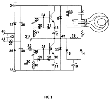
BRIEF DESCRIPTION OF THE FIGURES
The diagrams shown here help to understand as illustrative features of the
invention:
Fig.l is a complete diagram of the inverter voltage doubler rectifier and lamp
in the
circuit.
Fig.2 is a diagram illustrating the course of currents in the energized phase
inverter
element.
Fig.3 is a diagram illustrating the course of currents at the stage of de-
energized
elements of the inverter.
Fig. 4 is a diagram illustrating an electric arc lamp in the stage of a
malfunction at the
end of its useful life.
CA 02780685 2012-05-10
Fig. 5 shows the tubular core transformer in detail.
Fig. 6 shows an image of an electrical discharge in the lamp at the end of his
life,
obtained through digitizing oscilloscope and camera 2255 model tester AM503B
DC501
and current amplifier.
Fig. 7 shows the current in the lamp in normal operation, during its lifetime
obtained
with the same team.
Fig. 8 shows how you can connect more than one lamp to the circuit in Figure 1
by
adding the capacitor 44 in series with the lamp 49 and the positive side (+)
34, the
capacitor 46 in series with the filament 45 and filament 47 and the inductor
48, in
parallel with the inductance 7.
DETAILED DESCRIPTION OF THE INVENTION
Referring to Fig. 1, diodes, 8 and 22, commonly called free-bearing, which are
usually
built by the manufacturer in the body of the transistor used to protect the
peak-inverse
voltage. In order to have greater response in these diodes in the invention
connects the
diode 8, the positive (+) 34, point 43, excluding the resistor 12 and diode
22, negative (-)
35, to the point 43, excluding the resistance 11.
The operation of the starting circuit of the inverter is as follows: Once the
circuit
connected at the source of AC power at points 40 and 41, capacitors 38 and 39,
due to
6
CA 02780685 2012-05-10
the rectifier diodes 36 and 37 as known, between the point negative (-) 35
and, the
positive (+) 34, there is a full-wave rectified voltage twice the voltage of
AC power.
Based on the positive side (+) 34, the condenser 2, the filament 3, the
condenser 4, and
6 both filament lamp 5, the inductance 7, the primary winding 19, the
resistance 31 and
the capacitor 30 closes the circuit at the negative (-) 35, and when the
capacitor 30, is
energized, the diac 32 is placed on letting conducting state current at the
point 25 which
is the base of the transistor 9, the issuer that is the point 10, and through
the resistance
11, negative (-) 35. As the transistor 9, begins to conduct.
In order to give greater clarity to the investor behavior of this particular
operation is
considered in two stages: energizing stage and the stage of de-energization.
Once the driver to start driving transistor 9, In Fig.2 one can observe in
detail the
energization of the inverter stage, which begins at the point positive (+) 34,
where the
current passes through the condenser 2 and through strand 3, the condenser 4,
and the
filament 6, both of the lamp 5, while between these filaments of the lamp 5,
making the
electric arc passes through the inductor 7, the primary winding 19 by the
collector the
transistor 9, and its emitter 10, 11 resistance, and negative (-) 35.
Simultaneously, the
primary winding 19 magnetically coupled to the tubular core transformer for
simplicity
not drawn into the channels and clearly shown in Fig.5, which induces a
voltage in the
secondary winding 18, Fig 2, which generates the current flowing through the
resistor
26, and the point 25, which is the base of the transistor 9, paragraph 10,
which is the
issuer and the resistance 11, closing the circuit at the secondary winding 18,
bringing the
7
CA 02780685 2012-05-10
transistor 9, at maximum driving and therefore the maximum discharge lamp 5.
The
current generated in the secondary winding 18, circulates in positive
direction, ie in the
same direction as clockwise as illustrated in Figure 2. Simultaneously by
opposing
secondary winding 17, generating a current through the resistor 12, for item
13, the
diode 21 and the diode 20, closing the circuit at the secondary winding 17
antagonist. As
you can see, the point 13, which is the emitter of the transistor 1 has
greater potential
than the point 24, which is the base of transistor 1, so that the transistor
does not
conduct, being energized, the capacitor 2 and the condenser 4. This stage
concludes
energizing the inverter when the tubular core of the transformer Fig.5, is
saturated.
In that instant you start the cycle of de-energizing reversing a principle
known in the
inverter currents Fig.3, antagonist in the secondary winding 17, generating a
current
flowing in the positive direction, which passes through the resistor 23, for
Item 24 is the
base of transistor 1, point 13 which is the emitter of the transistor 1, and
the resistor 12,
closing the circuit at the secondary winding 17 antagonist, this current acts
on the
transistor 1, putting it in your state of maximum driving. Simultaneously in
the
secondary winding 18, generates a current that flows from the negative through
the
resistor 11, at point 10, the diode 28, through diode 29, closing the circuit
at the
secondary winding 18. As you can see the point 10 is more positive than about
25, so
that the transistor 9 can not drive and the stage of de-energization of the
investor ends
when the capacitor 2 and the capacitor 4 is discharged completely.
8
CA 02780685 2012-05-10
The stages of energizing and de-energization in the discharge of the lamp
currents and
voltages are sinusoidal, corresponding energizing phase inverter to the
positive side of
the sinusoid, and the stage of de-energizing the negative side. The system
operating
frequency is determined by the total value of capacitance and inductance that
contain
inverter circuits, and can be calculated using the formula known for resonant
circuits.
As shown in Fig. 2, and Fig.3, in the circuits for driving and driving in non-
Transistor 1
and 9, the currents induced change their meaning in harmony but not
interrupted for
the purpose of no discharges and transients generated within the circuit
itself can affect
the proper operation of the inverter, improving its operation up to three
percent
compared to current investors. Fig.4 is a diagram illustrating the behavior of
the
currents generated by malfunction of the lamp 5, the end of life, non-
symmetrical shock
and at a frequency higher than normal operation. As you can see the current
point of
the positive (+) 34, passing through the condenser 2, the filament 3, the
condenser 4,
the filament 6, the discharge of a malfunction of the lamp 5, through the
inductor 7, and
the primary winding 19, which has the necessary and sufficient inductive
reactance to
limit these current waveforms.
These lengthy downloads generate heat in the primary winding 19, in order to
avoid
these warm, this invention has a circuit of two high recovery diodes 14 and
15, whose
anodes are directly connected respectively to the ends of primary winding 19,
and
cathodes which are linked together connected to a resistor 16, where its other
end is
directly connected to the negative potential of the circuit point 35, and thus
is able to
9
CA 02780685 2012-05-10
send negative (-) 35, more frequent discharges to the stipulated so the
primary winding
19 can not induce enough voltage in the secondary winding 17 antagonist, so
that it can
generate enough current to make the transistor driver 1 and the condenser 2
and the
condenser 4, can not be downloaded what the investor ceases to oscillate. For
very low
power lamps under 10 watts, heating of the primary winding 19, is not very
strong so
that cost savings can eliminate high recovery rectifiers 14 and 15 and the
resistor 16, as
the circuit ceases to operate due to the inductive reactance of the primary
winding to
the position of the resistance 31, Fig.l not send start signal, the capacitor
being charged
2 and 4, having an abnormality or malfunction of the lamp in with the patent.
Once connected a new lamp button is pressed manually contact 33, Fig.l,
normally open
position so that the capacitor 2 and the capacitor 4 through the strands 3 and
6, the
new lamp 5, download and return the investor to operate as normal.
For the capacitors 2 and 4, remain energized and the inverter stops scrolling
in case of
malfunction of the lamp 5, it is necessary that the resistance 31, is
connected across the
primary winding 19, the inductance 7, strands 3 and 6, the lamp 5 and the
capacitor 4
and 2, the positive (+) 34 in the old technology the resistance 31 is directly
connected to
the feeder pole 34 or 35, so the diac 32, will be sending impulses causing the
transistor
9, the driver no matter what the discharge lamp, as investors continue
swinging to
prevent the transistor 9, stop driving discharging the capacitor 2 and the
capacitor 4
through the transistor 1.
CA 02780685 2012-05-10
The characteristic high inductive reactance of the tubular core transformer
Fig.5, the
minimum is achieved by maintaining the path of the magnetic field lines at its
core, this
dimension is limited in its inner diameter to space windings requiring three
turns with
minimal and to reduce the reluctance of the core is necessary to increase the
cross
sectional area without increasing the magnetic flux path and this is achieved
by
increasing the longer side of its cross section, so that said core acquires
its tubular shape
and its length is increases to a limit such that the resulting inductive
reactance does not
decrease the resonant frequency of design, as well as to limit discharges of
higher
frequency to pass through its windings.
The capacitor 42 and inductor 27 form a filter to protect the inverter circuit
on
phenomena that occur in the line of AC power connected to points 40 and 41.
Values of a circuit illustrating the invention Fig. 1 and Fig 8.
We present two cases 17 Watts and 80 Watts to illustrate the scope that has
the
invention.
Voltage doubler to 120 volts AC power in both cases.
For a lamp of 17 Watts For two lamps of 40 Watts
1, 9, Transistor 1, 9, Transistor
MJE 13007 To 220 MJE 13007 To 220
2, capacitor polyester 2, 44, polyester capacitor
.047 UF to 400v .047 uF to 400v
11
CA 02780685 2012-05-10
4, polyester capacitor 4, 46, polyester capacitor
.0039 UF at 1600V .021 uF at L600V
38, 39 electrolytic capacitor 38, 39 electrolytic capacitor
22uF a 250v IOOuF a 250v
7, Inductance 4.27 mH 7, 48, inductance 2.86 mH
11, 12 9 ohms Resistance 11, 12 9 ohms Resistance
Diode AR Diode AR
14, 15, 8, 20, 21, 22, 28, 29, 14, 15, 8, 20, 21, 22, 28, 29,
36, 37 Diode 1N4007 36 37 1N4007 diode
16, 6.6 megohms Resistance 16, Resistance 70 kohms
23, 26, 6.8 ohms Resistance 23, 26, 6.8 ohms Resistance
30, ceramic capacitor 30 ceramic capacitor
.014 UF at 600v .0047 u F at 600V
31, 50 k ohms Resistance 31, 100 k ohms Resistance
32, DIAC DB3 32 DIAC DB3
A core transformer of a tubular shape A core transformer of a tubular shape
.122 "x.111" x.244" 314" x.227 "x.347"
primary coil primary coil
two windings two windings
secondary coil secondary coil
three windings three windings
27 Inductance Capacitor O1mH 27 Inductance Capacitor O1mH
12
CA 02780685 2012-05-10
42 Polyester Capacitor 42 Polyester Capacitor
.047 u F 600v .047 u F 600v
13