Note: Descriptions are shown in the official language in which they were submitted.
CA 02783380 2012-06-06
WO 2011/106203 PCT/US2011/024948
SPALLING FOR A SEMICONDUCTOR SUBSTRATE
CROSS-REFERENCE TO RELATED APPLICATION
[0001] This application claims the benefit of U.S. Provisional Application No.
61/185,247, filed June 9, 2009. This application is also related to attorney
docket
numbers Y0R920100056U51, Y0R920100058U51, Y0R920100060U51, and
FIS920100006US1, each assigned to International Business Machines Corporation
(IBM)
and filed on the same day as the instant application, all of which are herein
incorporated
by reference in their entirety.
FIELD
[0002] The present invention is directed to semiconductor substrate
fabrication
using stress-induced substrate spalling.
DESCRIPTION OF RELATED ART
[0003] A large portion of the cost of a semiconductor-based solar cell may be
due
to the cost of producing a layer of a semiconductor substrate on which to
build the solar
cell. In addition to the energy costs associated with the separation and
purification of the
substrate material, there is a significant cost associated with the growth of
an ingot of the
substrate material. To form a layer of the substrate, the substrate ingot may
be cut using a
saw to separate the layer from the ingot. In the process of cutting, a portion
of the
semiconductor substrate material may be lost due to the saw kerf.
SUMMARY
[0004] In one aspect, a method for spalling a layer from an ingot of a
semiconductor substrate includes forming a metal layer on the ingot of the
semiconductor
substrate, wherein a tensile stress in the metal layer is configured to cause
a fracture in
the ingot; and removing the layer from the ingot at the fracture.
Page 1 of 11
CA 02783380 2012-06-06
WO 2011/106203 PCT/US2011/024948
[0005] In one aspect, a system for spalling a layer from an ingot of a
semiconductor substrate includes a metal layer formed on the ingot of the
semiconductor
substrate, wherein a tensile stress in the metal layer is configured to cause
a fracture in
the ingot, and wherein the layer is configured to be removed from the ingot at
the
fracture.
[0006] Additional features are realized through the techniques of the present
exemplary embodiment. Other embodiments are described in detail herein and are
considered a part of what is claimed. For a better understanding of the
features of the
exemplary embodiment, refer to the description and to the drawings.
BRIEF DESCRIPTION OF THE SEVERAL VIEWS OF THE DRAWINGS
[0007] Referring now to the drawings wherein like elements are numbered alike
in the several FIGURES:
[0008] FIG. 1 illustrates an embodiment of method for spalling for an ingot of
a
semiconductor substrate.
[0009] FIG. 2 illustrates an embodiment of an ingot of a semiconductor
substrate
with a seed layer.
[0010] FIG. 3 illustrates an embodiment of an ingot of a semiconductor
substrate
with an adhesion layer.
[0011] FIG. 4 illustrates an embodiment of a system for forming a stressed
metal
layer on an ingot of a semiconductor substrate.
[0012] FIG. 5 illustrates an embodiment of an ingot of a semiconductor
substrate
with a stressed metal layer.
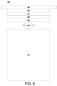
[0013] FIG. 6 illustrates an embodiment of a spalled layer of an ingot of a
semiconductor substrate.
Page 2 of 11
CA 02783380 2012-06-06
WO 2011/106203 PCT/US2011/024948
[0014] FIG. 7 illustrates a top view of an embodiment of a spalled layer of an
ingot of a semiconductor substrate.
DETAILED DESCRIPTION
[0015] Embodiments of systems and methods for spalling for a semiconductor
substrate are provided, with exemplary embodiments being discussed below in
detail.
[0016] A layer of tensile stressed metal or metal alloy may be formed on a
surface
of an ingot of a semiconductor material to induce a fracture in the ingot by a
process
referred to as spalling. A layer of the semiconductor substrate having
controlled
thickness may be separated from the ingot at the fracture without kerf loss.
The stressed
metal layer may be formed by electroplating or electroless plating. Spalling
may be used
to cost-effectively form layers of semiconductor substrate for use in any
semiconductor
fabrication application, such as relatively thin semiconductor substrate
wafers for
photovoltaic (PV) cells, or relatively thick semiconductor-on-insulator for
mixed-signal,
radiofrequency (RF), or microelectromechanical (MEMS) applications.
[0017] FIG. 1 illustrates an embodiment of a method 100 for spalling for an
ingot
of a semiconductor substrate. FIG. 1 is discussed with reference to FIGS. 2-7.
The
semiconductor material comprising the ingot may comprise germanium (Ge), or
single-
or poly-crystalline silicon (Si) in some embodiments, and may be n-type or p-
type. For
an n-type semiconductor material, block 101 is optional. In block 101, a
surface of an
ingot 201 of a semiconductor material that is to be spalled is pre-treated by
forming a
seed layer 202 on the surface of the ingot, as is shown in FIG. 2. The seed
layer 202 is
necessary for an ingot 201 of p-type semiconductor material (in which holes
are the
majority carriers), as direct electroplating on p-type material is difficult
due to the surface
depletion layer that may be formed when a p-type ingot 201 is subjected to a
negative
bias with respect to the electroplating solution. The seed layer 202 may
comprise a single
layer or multiple layers, and may comprise any appropriate material. The seed
layer 202
may comprise palladium (Pd) in some embodiments, which may be applied to ingot
201
Page 3 of 11
CA 02783380 2012-06-06
WO 2011/106203 PCT/US2011/024948
via immersion in a bath comprising a Pd solution. In other embodiments, in
which the
ingot 201 comprises Si, formation of the seed layer 202 may comprise forming a
layer of
titanium (Ti) on ingot 201, and forming a silver (Ag) layer over the Ti layer.
The Ti and
the Ag layers may each be less than about 20 nanometers (nm) thick. Ti may
form a
good adhesive bond to Si at low temperature, and the Ag surface resists
oxidation during
electroplating. The seed layer 202 may be formed by any appropriate method,
including
but not limited to electroless plating, evaporation, sputtering, chemical
surface
preparation, physical vapor deposition (PVD), or chemical vapor deposition
(CVD). The
seed layer 202 may be annealed after formation in some embodiments.
[0018] In block 102, an adhesion layer 301 of a metal is formed on the ingot
201.
For embodiments comprising a p-type ingot 201, the adhesion layer 301 is
optional, and
formed over the seed layer 202 as is shown in FIG. 3. For embodiments
comprising an n-
type ingot 201, the adhesion layer is formed directly on the ingot 201, and
there is no
seed layer 202. The adhesion layer 301 may comprise a metal, including but not
limited
to nickel (Ni), and may be formed by electroplating or by any other
appropriate process.
The adhesion layer 301 may be less than 100 nm thick in some embodiments.
Formation
of the adhesion layer 301 may be followed by annealing to promote adhesion
between the
metal adhesion layer 301, the seed layer 202 (for p-type semiconductor
material), and
semiconductor ingot 201. Annealing causes the adhesion layer 301 to react with
the
semiconductor material 201. Annealing may be performed at a relatively low
temperature, below 500 C in some embodiments. Inductive heating may be used
for
annealing process in some embodiments, allowing heating of the metal adhesion
layer
301 without heating the ingot 201.
[0019] In block 103, electroplating (or electrochemical plating) is performed
by
immersing the surface of ingot 201 comprising adhesion layer 301 in a plating
bath 401,
and applying a negative bias 402 with respect to plating bath 401 to the ingot
201, as is
shown in FIG. 4. The plating bath 401 may comprise any chemical solution
capable of
depositing a stressed metal layer 501 (as shown in FIG. 5) on the ingot 201
either
Page 4 of 11
CA 02783380 2012-06-06
WO 2011/106203 PCT/US2011/024948
autocatalytically (electroless) or upon application of external bias 402. In
an exemplary
embodiment, plating bath 401 comprises a 300 gram/liter (g/1) aqueous solution
of NiC12
with 25 g/1 of boric acid. The plating bath temperature may be between 0 C and
100 C in
some embodiments, and between 10 C and 60 C in some exemplary embodiments. The
plating current flowing in ingot 201 during electroplating may vary; however,
the plating
current may be about 50mA/cm2 in some embodiments, yielding a deposition rate
of
about 1 micron/min. Prior to electroplating, if any oxide layers have formed
on adhesion
layer 301, these oxide layers may be removed chemically. For example, a
diluted HC1
solution may be used to remove oxide layers from an adhesion layer 301
comprising Ni.
[0020] Electroplating causes stressed metal layer 501 to form on adhesion
layer
301, as is shown in FIG. 5. FIG. 5 shows an embodiment of an ingot 201
comprising p-
type semiconductor material, with a seed layer 202. If the ingot 201 comprises
n-type
semiconductor material, seed layer 202 is not present. The stressed metal
layer 501 may
be between 1 and 50 microns thick in some embodiments, and in between 4 and 15
microns thick in some exemplary embodiments. The tensile stress contained in
metal
layer 501 may be greater than about 100 megapascals (MPa) in some embodiments.
[0021] In block 104, semiconductor layer 601 is separated from ingot 201 via
spalling at fracture 603, as is shown in FIG. 6. FIG. 6 shows an embodiment of
an ingot
201 comprising p-type semiconductor material, having a seed layer 202. If the
ingot 201
comprises n-type semiconductor material, seed layer 202 is not present.
Spalling may be
used in conjunction with an ingot 201 having any crystallographic orientation;
however,
fracture 603 may be improved in terms of roughness and thickness uniformity if
fracture
603 is oriented along the natural cleavage plane of the material comprising
ingot 201
(<111> for Si and Ge).
[0022] Spalling may be either controlled or spontaneous. In controlled
spalling
(as shown in FIG. 6), a handle layer 602 is applied to the metal layer 501,
and is used to
induce fracture in the ingot 201 to remove the semiconductor layer 601 from
the ingot
Page 5 of 11
CA 02783380 2012-06-06
WO 2011/106203 PCT/US2011/024948
201 along fracture 603. The handle layer 602 may comprise a flexible adhesive,
which
may be water-soluble in some embodiments. Use of a rigid material for the
handle layer
602 may render the spalling mode of fracture unworkable. Therefore, the handle
layer
602 may further comprise a material having a radius of curvature of less than
5 meters in
some embodiments, and less than 1 meter in some exemplary embodiments. In
spontaneous spalling, the stress contained in the stressed metal layer 501
causes
semiconductor layer 601 and the stressed metal layer 501 to spontaneously
separate
themselves from the ingot 201 at a fracture, without the use of a handle layer
602.
Controlled spalling may be made to become spontaneous spalling upon heating of
the
stressed metal 501. Heating tends to increase the tensile stress in the
stressed metal 501,
and can initiate spontaneous spalling. Heating may be performed in any
appropriate
manner, including but not limited to a lamp, laser, resistive, or inductive
heating.
[0023] FIG. 7 illustrates a top view of an embodiment of a semiconductor layer
601 on a handle layer 602. The handle layer 602 may be removed, and stressed
metal
layer 501, adhesion layer 301, and seed layer 202 (in the case of a p-type
ingot 201) may
be etched off, depending on the application for which semiconductor layer 601
is to be
used. Semiconductor layer 601 may have any desired thickness, and be used in
any
desired application. Semiconductor layer 601 may comprise single- or poly-
crystalline
silicon in some embodiments.
[0024] In block 105, blocks 101-104 may be repeated using ingot 201. Because
there is no kerf loss, layers of the ingot 201 may removed from the ingot 201
with
relatively little waste, maximizing the number of layers of a semiconductor
material that
may be formed from a single ingot.
[0025] The technical effects and benefits of exemplary embodiments include
reduction of waste in semiconductor fabrication.
[0026] The terminology used herein is for the purpose of describing particular
embodiments only and is not intended to be limiting of the invention. As used
herein, the
Page 6 of 11
CA 02783380 2012-06-06
WO 2011/106203 PCT/US2011/024948
singular forms "a", "an", and "the" are intended to include the plural forms
as well, unless
the context clearly indicates otherwise. It will be further understood that
the terms
"comprises" and/or "comprising," when used in this specification, specify the
presence of
stated features, integers, steps, operations, elements, and/or components, but
do not
preclude the presence or addition of one or more other features, integers,
steps,
operations, elements, components, and/or groups thereof.
[0027] The corresponding structures, materials, acts, and equivalents of all
means
or step plus function elements in the claims below are intended to include any
structure,
material, or act for performing the function in combination with other claimed
elements
as specifically claimed. The description of the present invention has been
presented for
purposes of illustration and description, but is not intended to be exhaustive
or limited to
the invention in the form disclosed. Many modifications and variations will be
apparent
to those of ordinary skill in the art without departing from the scope and
spirit of the
invention. The embodiment was chosen and described in order to best explain
the
principles of the invention and the practical application, and to enable
others of ordinary
skill in the art to understand the invention for various embodiments with
various
modifications as are suited to the particular use contemplated.
INDUSTRIAL APPLICABILITY
[0028] This invention finds utility in the fabrication of semiconductor
substrates.
Page 7 of 11