Note: Descriptions are shown in the official language in which they were submitted.
CA 02802219 2012-12-11
WO 2012/009812 PCT/CA2011/050442
MULTIPAGE PROGRAM SCHEME FOR FLASH MEMORY
TECHNICAL FIELD
[0001] The present invention relates to generally a semiconductor device and
in
particular to programming multiple bits of data to a single flash memory cell.
BACKGROUND
[0002] Flash memory is a commonly used type of non-volatile memory in
widespread use as mass storage for consumer electronics, such as digital
cameras and
portable digital music players for example. The density of a presently
available flash
memory chip can be up to several Gbytes (GB) in size, which is suitable for
use in
popular USB flash drives since the size of one flash chip is small. Another
emerging
application for flash memory are solid state drives for replacing traditional
hard disk drives
used in laptop and desktop computers.
[0003] Figure 1 is a general block diagram of typical flash memory device
known
in the art. Flash memory device 10 includes input/output interface circuits,
control circuits,
memory circuits and a memory array. The input/output interface circuits of
flash memory
device 10 include a Ready/Busy signal buffer 12, control signal buffers 14 and
global data
buffers 16. The Ready/Busy signal buffer 12 is an output buffer which drives
the
Ready/Busy signal R/B# via a respective pin or port. In the present example,
the control
signal buffers 14 are input buffers which receive flash memory control signals
CE#, CLE,
ALE, WE#, RE# and WP# from corresponding pins or ports. Signal names ending
with "#"
should be understood from this point forward as being active low level
signals, where an
active low signal corresponds to a "0" logic level, or a VSS voltage level for
example. In
contrast, an active high logic level signal corresponds to a "1" logic level,
or a VDD or
VCC voltage level for example. Following is a short description of the
previously
mentioned control signals.
= Command Latch Enable (CLE): the CLE input signal is used to control loading
of
the operation mode command into the internal command register. The command
is latched into the command register from the I/O port on the rising edge of
the
WE# signal while CLE is High.
-1-
CA 02802219 2012-12-11
WO 2012/009812 PCT/CA2011/050442
= Address Latch Enable (ALE): the ALE signal is used to control loading
address
information into the internal address register. Address information is latched
into
the address register from the I/O port on the rising edge of the WE# signal
while
ALE is High.
= Chip Enable (CE#): the device goes into a low-power Standby mode when CE#
goes High during the device is in Ready state. The CE# signal is ignored when
device is in Busy state (R/B# = L), such as during a Program or Erase or Read
operation, and will not enter Standby mode even if the CE# input goes High.
= Write Enable (WE#): the WE# signal is used to control the acquisition of
data
from the I/O port.
= Read Enable (RE#): the RE signal controls serial data output. Data is
available
after the falling edge of RE#. The internal column address counter is also
incremented (Address = Address + I) on this falling edge.
= I/O Port (1/00 to 7): 1/00 to 7 pins are used as a port for transferring
address,
command and input/output data to and from the device.
= Write Protect (WP#): the WP# signal is used to protect the device from
accidental programming or erasing. The internal voltage regulator (high
voltage
generator) is reset when WP# is Low. This signal is usually used for
protecting the
data during the power-on/off sequence when input signals are invalid.
= Ready/Busy (R/B#): the R/B# is open drain pin and the output signal is used
to
indicate the operating condition of the device. The R/B# signal is in Busy
state
(R/B# = L) during the Program, Erase and Read operations and will return to
Ready state (R/B# = H) after completion of the operation.
[0004] The global data buffers 16 in the present example of Figure 1 are bi-
directional buffers which receive write data and provide read data on
respective
input/output (I/O) pins or ports. The flash memory device 10 is shown to have
8 such
ports 1/00 to 1/07, but can have more or less than 8 in alternate data width
configurations.
These I/O ports are also used for receive address and command information.
[0005] The control circuits of flash memory device 10 include controller 18,
command register 20, address register 22 and status register 24. Controller 18
controls
various functions of the other circuits in flash memory device 10, where such
functions
include read, program and program verification. While not shown, the
controller 18 can
include a command decoder for executing the functions in response to a
received
command. The registers store types of information received by flash memory
device 10 or
to be provided to an external host system, including a memory controller for
example. The
-2-
CA 02802219 2012-12-11
WO 2012/009812 PCT/CA2011/050442
described registers are not intended to be exhaustive, and other registers can
be
included, such as data registers for example.
[0006] The circuits primary controlled by controller are the memory circuits,
which
include row and column pre-decoders 26 and 28, row and column decoders 30 and
32,
sense amplifiers and page buffer block 34, and a high voltage generator 36.
The memory
array 38 of flash memory device 10 consists of NAND cell strings connected to
bitlines,
where each memory cell of a NAND cell string is connected to a wordline.
Further details
of a NAND cell string is shown later in Figure 3. The row pre-decoder 26, row
decoder 30
and high voltage generator 36 are controlled in a programming operation to
drive a
selected wordline to a high voltage effective for shifting a threshold voltage
of the
connected memory cell from a default erased threshold voltage to a desired
voltage level.
It is noted that a high voltage may be used in the memory array 38 to erase
memory cells
by shifting their threshold voltages to the default value. Different
combinations of high
voltages and applied time of the high voltages can be used to set specific
threshold
voltages for a flash memory cell. A combination for programming a specific
threshold
voltage can be referred to as a programming profile. The page buffer 34 stores
a page of
data to be programmed to the cells connected to the selected wordline.
Generally, a
memory cell connected to a bitline is either inhibited from being programmed
or enabled
for programming via the selected wordline, depending on the logic level the
bitline is
biased, or set to. The data bits stored in the page buffer are used to bias
the bitline.
[0007] Figure 2 is a threshold voltage distribution graph for a single bit
flash
memory cell, which stores one of two possible levels or states, State 0 or
State 1. This is
also referred to as single level cell (SLC) memory. In Figure 2, State 0 is
the default
erased state of all flash memory cells of memory array 38, which in this
example is a
negative threshold voltage. In contrast, State 1 corresponds to a positive
threshold
voltage. Therefore when erased, the flash memory cells stores the "1" logic
state for a
single bit of stored data. Programming is then executed to shift the erased
threshold
voltage to the positive voltage of State 1 if the data to be stored in a
selected cell
corresponds to a "0", which as previously explained is done by driving the
selected
wordline connected to the cell with a particular programming profile.
[0008] Figure 3 is a circuit schematic showing a portion of memory array 38 of
Figure 1, and in particular shows NAND cell strings connected to two bitlines
BL1 and
BLj. Each NAND cell string has flash memory cells 50 serially coupled arranged
and
electrically coupled to each other. Accordingly, wordlines WLO to WLi are
coupled to the
-3-
CA 02802219 2012-12-11
WO 2012/009812 PCT/CA2011/050442
gates of each flash memory cell 50 in the memory cell string. Place holders
"i" and "j" are
integer values, designating a last wordline and bitline respectively. A string
select device
52 coupled to signal SSL (string select line) selectively connects the memory
cell string to
a bitline (BL1 or BLj), while a ground select device 54 coupled to signal GSL
(ground
select line) selectively connects the memory cell string to a source line,
such as VSS. The
string select device 52 and the ground select device 54 are n-channel
transistors. The
two NAND cell strings shown in Figure 3 connected to the same wordlines, SSL
and GSL
are part of one memory block 56. Accordingly, there can be multiple memory
blocks
connected to the same bitlines BL1 to BLj in parallel to the memory block
shown in Figure
1.
[0009] If flash memory cells 50 store a single bit of data, then all the cells
50
connected to the same wordline store a page of data. In Figure 3 by example,
the cells
connected to WLO are collectively referred to physical Page 0, while the cells
connected
to WLj are collectively referred to as physical Page i, where each stores one
page of data.
[0010] Coupled to each bitline BL1 to BLj is a page buffer 58 for storing one
page
of data to be programmed into one page of flash memory cells. Page buffer 58
also
includes sense circuits for sensing data read from one page of flash memory
cells. During
programming operations, the data registers perform program verify operations
to ensure
that the data has been properly programmed into the flash memory cells coupled
to the
selected wordline. Therefore, each row of cells stores a page of data. To
achieve
improved density, each flash memory cell can store at least two bits of data,
and is
generally referred to as a multi-bit-cell (MBC). In storing at least two bits
of data per cell,
the storage density of a memory array is at least doubled relative to the same
memory
array having cells that store only one bit of data.
[0011] Figure 4 is a threshold voltage distribution graph for a two-bit flash
memory
cell. This is also referred to as multiple level per cell (MLC) memory. Figure
4 shows four
possible states, State 0, State 1, State 2 and State 3, which can be stored by
a two-bit
flash memory cell. As shown by example in Figure 4, each state corresponds to
a
combination of two bits of data. State 0 can represent binary values "11 ",
State 1 can
represent binary values "10", State 2 can represent binary values "00", and
State 3 can
represent binary values "01". The binary values shown in Figure 4 are example
combinations, and the assignment of binary value combinations for each state
can differ
from those presently shown in Figure 4. Accordingly, a row of flash memory
cells
connected to the same wordline can now store two pages of data, instead of the
single
page of data for the single bit flash memory cell. The logical organization of
these two
-4-
CA 02802219 2012-12-11
WO 2012/009812 PCT/CA2011/050442
pages of data, referred to as logical pages, associated with cells connected
to a common
wordline, referred to as a physical page, is now described.
[0012] Figure 5 is an illustration showing storage of lower and upper pages of
data stored in rows of two-bit flash memory cells. In Figure 5, flash memory
cells 70 and
72 are part of a first NAND cell string, flash memory cells 74 and 76 are part
of a second
NAND cell string, flash memory cells 78 and 80 are part a last NAND cell
string,
representing the last NAND cell string in a memory block. Depending on the
configuration
of the block, there can be a plurality of intervening NAND cell strings
between the second
NAND cell string and the last NAND cell string. Each of the flash memory cells
has one of
the four possible logic states shown in Figure 4, with the corresponding two-
bit binary
value assignments. In the example of Figure 5, cell 70 stores State 3, cell 72
stores State
1, cell 74 stores State 1, cell 76 stores State 3, cell 78 stores State 2, and
cell 80 stores
State 0. The binary values are shown in each cell, where the upper bit
corresponds to the
left-most bit in the corresponding state of Figure 4 and the lower bit
corresponds to the
right-most bit. The flash memory cells 72, 76 and 80 connected to wordline WLO
correspond to a physical page having lower bits of flash memory cells 72, 76
and 80
correspond to logical page 0, while the upper bits correspond to logical page
1. Similarly,
the flash memory cells 70, 74 and 78 connected to wordline WLi correspond to
another
physical page having lower bits corresponding to logical page k-1, while the
upper bits
correspond to a last logical page k. Therefore, it can be seen how each
physical page
stores two pages of data.
[0013] By extension, if each flash memory cell can store 3 bits of data, then
each
cell can store 23 = 8 states, which means that each physical page can store up
to 8 pages
of data. Provided all the different states can be programmed and sensed during
a read
operation, the increase in storage density without the need for increasing the
physical
memory array size affords significant advantages for mass storage
applications.
Unfortunately, the time required for programming two pages of data (two bits
per cell) per
physical page is significantly increased relative to programming a single page
of data per
physical page. This increased programming time is further exacerbated if 3 or
more bits
per cell storage is used.
[0014] While the time required for occasionally copying several small data
files to
a USB drive capable of multiple bit per cell storage may not appear
inconvenient for
users, the frequent writing of a large number of small data files will
noticeably take a
longer amount of time. Frequent writing of smaller data files is common in
solid state hard
-5-
CA 02802219 2012-12-11
WO 2012/009812 PCT/CA2011/050442
disk drives, which can impose a performance limitation on the computer system
it is used
within. Storage of larger data files such as music and video files to flash
memory capable
of storing multiple bits per cell will take a very noticeable duration of time
to program.
[0015] As flash memories are widely used in computing applications such as
Sods and flash cache, higher performance flash memories are desired. It should
be noted
that high performance operation can be obtained with one or more of higher I/O
bandwidth, higher read and write throughput and higher flexibility of
operations.
Moreover flash storage systems for computing applications require higher
memory
capacity without diminishing performance.
[0016] It is therefore desirable to reduce the time required for programming
cells
storing two or bits of data, to thereby improve overall performance of the
system it is used
within.
SUMMARY
[0017] In accordance with a first aspect, there is provided a multi-page
programming method for a NAND flash memory device. The method includes storing
M
pages of data in the NAND flash memory device, where M is an integer value
greater
than 1, and initiating a multi-page programming operation in the NAND flash
memory
device for storing up to 2M states in memory cells of the NAND flash memory
device.
According to one embodiment of the present aspect, the method can further
include
checking a completion status of the multi-page programming operation and
determining if
the multi-page programming operation was successful when the completion status
corresponds to a completed multipage programming operation. According to a
nether
embodiment of the present aspect, storing can include iteratively loading each
of the M
pages of data into respective M page buffers of the NAND flash memory device,
where
loading each of the M pages of data can include receiving at the NAND flash
memory
device, a data load command followed by input data. In the present
embodiments, the
input data includes the data and address information. Also in the present
embodiments,
the data load command is a first data load command, and a second data load
command
is received after the input data corresponding to the 1st data load command is
received.
In this embodiment, a data end command is received after the input data
corresponding
to the first data load command is received and before the second data load
command is
received. Alternately, a data end command fora last page of the M pages of
data is
-6-
CA 02802219 2012-12-11
WO 2012/009812 PCT/CA2011/050442
received after input data corresponding to the last page of the M pages of
data is
received, where the data end command includes a multi-page program command.
[0018] In another embodiment, the multi-page programming operation includes
executing 2M -1 programming iterations to program up to 2M -1 states and one
of the 2M
states is an erased state. Each programming iteration includes biasing each of
the bitlines
to enable or inhibit programming in response to a combination of bits of the M
pages of
data that correspond to each bitline. Furthermore, each programming iteration
includes
driving a selected wordline with a programming profile specific to each
programming
iteration while the bit lines are biased to enable or inhibit programming.
[0019] In a second aspect, there is provided a flash memory device. The flash
memory device includes a memory array, bitline access circuitry and row
circuits. The
memory array has flash memory cells connected to wordlines and coupled to
bitlines. The
bitline access circuitry stores M pages of data and biases the bitlines to
enable or inhibit
programming for each of 2M -1 programming iterations in response to a
combination of
bits corresponding to each bitline from the M pages of data, where M is an
integer
number of at least 2. The row circuits drive a selected wordline with a
programming
profile for each of the 2M -1 programming iterations while the bitlines are
biased to enable
or inhibit programming. According to an embodiment of the 2nd aspect, the
bitline access
circuitry includes M data buffers each for storing one of the M pages of data,
and bitline
biasing circuitry for biasing each of the bitlines to enable or inhibit
programming in
response to a combination of bits of the M pages of data stored in the M data
buffers that
correspond to each bitline. In this embodiment, each of the M data buffers
includes data
storage circuits for storing one bit of a page of data, and each bit position
of the M data
buffers includes a data verify decoder and inversion circuitry. The data
verify decoder
receives the bits of the M pages of data stored in the M data buffers that
correspond to
each bitline. The inversion circuitry inverts the bits in response to selected
outputs of the
data decoder.
[0020] In a third aspect, there is provided a flash memory device. The flash
memory device includes a memory array, a bitline access circuit, and row
circuits. The
memory array has flash memory cells connected to wordlines and coupled to
bitlines,
where each flash memory cell is programmable to have a threshold voltage
corresponding to one of an erase state, a first state, a second state and a
third state. The
bitline access circuit biases the bitlines to program the first state, the
second state and
the third state in a predetermined order. The bitline access circuit biases
the bitlines to
enable or inhibit programming for each of the first state, the second state
and the third
-7-
CA 02802219 2012-12-11
WO 2012/009812 PCT/CA2011/050442
state in response to specific combinations of bits from two pages of data. The
row circuits
drive a selected wordline with programming profiles corresponding to the first
state, the
second state and the third state while the bitline is biased for programming
the first state,
the second state and the third state respectively.
[0021] In a fourth aspect, there is provided a method for programming a flash
memory device. The method includes loading at least two pages of data into
page buffers
of the flash memory device; biasing bitlines of the flash memory device; and
driving a
wordline of the flash memory device. The bitlines of the flash memory device
are biased
to voltage levels effective for one of inhibiting programming and enabling
programming of
different threshold voltages to flash memory cells coupled to the bitlines in
response to
logic states of data bits of the at least two pages of data. The word line is
driven for a
period of time for programming the different threshold voltages to the flash
memory cells
that are connected to the wordline in parallel.
[0022] In a fifth aspect, there is provided a method for programming different
states to a plurality of flash memory cells in parallel. The method includes
receiving M bits
of data for each of the flash memory cells, where M is an integer value of at
least 2;
determining one state of 2M possible states to store in each of the plurality
of flash
memory cells in response to the M bits of data; biasing bit lines connected to
the plurality
of flash memory cells with predetermined voltage levels, where each
predetermined
voltage level corresponds to each of the 2M possible states; and driving a
selected word
line for programming up to 2M different states in the plurality of flash
memory cells in
parallel.
[0023] In a sixth aspect, there is provided a bitline modulator circuit for
multi-state
programming of pages of data to a physical page of flash memory cells. The
bitline
modulator circuit includes a program data decoder and a bitline biasing
circuit. The
program data decoder receives M bits of data and provides decoded selection
signals in
response to a logic combination of the M bits of data, where M is an integer
number of at
least 2 and each of the M bits of data is associated with one of the pages of
data. The
bitline biasing circuit biases a bitline to one of 2M voltage levels in
response to the
decoded selection signals.
[0024] In a seventh aspect, there is provided a flash memory device. The flash
memory device includes a memory array, M page buffers, bitline modulators and
row
circuits. The memory array has flash memory cells connected to wordlines and
coupled to
bitlines. The M page buffers store M pages of data, where M is an integer
number of at
least 2. The bitline modulators are coupled to each of the bitlines and to the
M page
-8-
CA 02802219 2012-12-11
WO 2012/009812 PCT/CA2011/050442
buffers. Each of the bitline modulators applies one of 2M voltage levels to a
corresponding
bitline in response to a combination of data bits from each of the M pages of
data. The
row circuits drive a selected wordline with a programming profile to program
the M pages
of data to a row of flash memory cells.
[0025] Other aspects and features of the present invention will become
apparent
to those ordinarily skilled in the art upon review of the following
description of specific
embodiments of the invention in conjunction with the accompanying figures.
BRIEF DESCRIPTION OF THE DRAWINGS
[0026] Embodiments of the present invention will now be described, by way of
example only, with reference to the attached Figures, wherein:
Figure 1 is a functional block diagram of a NAND flash memory device;
Figure 2 is a threshold voltage distribution graph for a single bit flash
memory cell;
Figure 3 is a circuit schematic showing NAND cell strings of a NAND flash
memory array;
Figure 4 is a threshold voltage distribution graph for a two-bit flash memory
cell;
Figure 5 is an illustration showing storage of lower and upper pages of
data stored in two-bit flash memory cells;
Figures 6A and 6B are graphical illustrations showing a sequence for
programming two-bit per cell data using two programming operations in NAND
flash;
Figure 7 illustrates an alternate sequence for programming two-bit per cell
data using two programming operations in NAND flash;
Figure 8 is a block diagram of a multi-page programmable NAND flash
memory, according to a present embodiment;
Figure 9 is a flow chart of a method of operating a flash memory device for
a multi-page program operation, according to a present embodiment;
Figure 10 is a flow chart of a method of operating a flash memory device
for a two-page multi-page program operation, according to a present
embodiment;
Figure 11 is a sequence diagram showing an example two-page multi-
page program operation of a flash memory device, according to a present
embodiment; Figure 12A is a sequence diagram showing an example command
-9-
CA 02802219 2012-12-11
WO 2012/009812 PCT/CA2011/050442
and data input sequence for a flash memory device, according to a present
embodiment;
Figure 12B is a sequence diagram showing an alternate example
command and data input sequence for a flash memory device, according to a
present embodiment;
Figure 13 is a flow chart of a method for programming all logic states to
MLC flash cells in a single programming operation cycle, according to a
present
embodiment;
Figure 14A is a sequence diagram showing a multi-page program
operation for programming logic states to flash cells connected to 4 different
bitlines, according to a present embodiment;
Figure 14B is a threshold voltage distribution graph showing threshold
voltages of the 4 flash cells programmed in Figure 14A;
Figure 15A is a sequence diagram showing an alternate multi-page
program operation for programming logic states to flash cells connected to 4
different bitlines, according to a present embodiment;
and,
Figure 15B is a threshold voltage distribution graph showing threshold
voltages of the 4 flash cells programmed in Figure 15A;
Figure 16 is a block diagram of the bitline access circuitry shown in Figure
8, according to a present embodiment;
Figure 17 is a schematic showing details of the data decoder of Figure 16,
according to a present embodiment;
Figure 18A is a sequence diagram showing a two-page parallel multi-page
program operation of a flash memory device, according to a present embodiment;
Figure 18B is a threshold voltage distribution graph showing example
threshold voltages of flash cells programmed in Figure 18A;
Figure 19A is a sequence diagram showing an alternate two-page parallel
multi-page program operation of a flash memory device, according to a present
embodiment;
Figure 19B is a threshold voltage distribution graph showing example
threshold voltages of flash cells programmed in Figure 19A;
Figure 20A is a sequence diagram showing an alternate two-page parallel
multi-page program operation of a flash memory device, according to a present
embodiment;
-10-
CA 02802219 2012-12-11
WO 2012/009812 PCT/CA2011/050442
Figure 20B is a threshold voltage distribution graph showing example
threshold voltages of flash cells programmed in Figure 20A;
Figure 21 is a flow chart illustrating a program inhibit method for flash
memory cells;
Figure 22A is cross sectional view of a NAND cell string;
Figure 22B is a sequence diagram illustrating an example of the program
inhibit method of Figure 21;
Figure 23 is a circuit schematic showing example voltage biasing of bitlines
for parallel multi-state programming, according to a present embodiment;
Figure 24 is a block diagram of bitline access circuitry for parallel multi-
state programming, according to a present embodiment;
Figure 25 is a schematic showing the functional blocks of the bitline
modulator shown in Figure 24, according to a present embodiment;
Figure 26 is a circuit schematic embodiment of the program data decoder
shown in Figure 25, according to a present embodiment;
Figure 27 is a circuit schematic embodiment of the bitline biasing circuit
shown in Figure 25; and
Figure 28 is a circuit schematic embodiment of a control circuit for the
multi-state programming embodiment of Figure 18A; and,
Figure 29 is a flowchart outlining a method for parallel multi-state
programming, according to a present embodiment.
DETAILED DESCRIPTION
[0027] The present invention generally relates to methods to program multiple
logical pages of data to one physical page of cells in a single programming
cycle in flash
memory. In particular, a circuit and method for programming multiple bits of
data to flash
memory cells in a single program operation cycle are described. Multiple pages
of data to
be programmed into one physical page of a flash memory array are stored in
page
buffers or other storage means on the memory device. The selected wordline
connected
to the cells to be programmed is driven with predetermined program profiles at
different
time intervals, where each predetermined program profile is configured for
shifting an
erase threshold voltage to a specific threshold voltage corresponding to a
specific logic
state. The bit lines are biased to specific states during each of the time
intervals, in
-11-
CA 02802219 2012-12-11
WO 2012/009812 PCT/CA2011/050442
response to the combination of specific logic states of the bits belonging to
each page of
data that are associated with that respective bitline.
[0028] Preferred embodiments are implemented in NAND flash memory although
the present invention may be applicable to other type of flash memory such as,
for
example, NOR flash memory.
[0029] Prior to a discussion of the embodiments, current MLC programming
schemes will now be described. A common MLC flash memory architecture is the 2
bit
per cell flash memory. Therefore, current 2 bit per cell programming schemes
are
described. In a 2 bit per cell scheme, each wordline within a NAND cell string
is decoded
into two logical pages as a first page (a lower page) and a second page (an
upper page).
With reference to Figure 5, logical page 0 can be a lower page while logical
page 1 can
be an upper page. In this example, the lower page is first programmed,
followed by
programming of the upper page. This sequence is illustratively shown in
Figures 6A and
6B.
[0030] Figure 6A is a threshold voltage distribution graph showing logic
states
corresponding to a first bit of data (1 or 0) to be stored in a 2 bit flash
memory cell. Prior
to programming, all cells of a memory block are erased. Figure 6A shows the
erased
state to be State 0, which in the present example is a negative threshold
voltage. In a
first program operation cycle, the bit corresponding is programmed to State 1,
or it
remains at State 0 depending on the logic state of the bit to be stored.
Figure 6B is
another threshold voltage distribution graph showing the possible sequence for
programming a second bit of data (1 or 0), also referred to as the bit of the
upper page, to
the cell programmed in Figure 6A. In a subsequent programming cycle, this
second bit
corresponding to the upper page is programmed. The logic state of this second
bit
determines if and how State 2 and State 3 are programmed. If for example State
0 and
State 1 have the binary assignments shown in Figure 4, and the second bit to
be
programmed (left-most bit) is a logic 1, then there is no need to program
State 2 or State
3 because both State 0 and State 1 have an upper bit assigned to a logic 1. On
the other
hand, programming of State 2 or State 3 is required if the second bit to be
programmed is
a logic 0.
[0031] In programming State 2 or State 3 of the present example, the logic
state
of the originally programmed lower bit is retained. Therefore, as shown in
Figure 6B, the
threshold voltage corresponding to State 0 is shifted to the threshold voltage
corresponding to State 3 or the threshold voltage corresponding to State 1 is
shifted to
the threshold voltage corresponding to State 2. Therefore, the shown logic
states State 0
-12-
CA 02802219 2012-12-11
WO 2012/009812 PCT/CA2011/050442
to State 3 encode the different logic combinations of the upper and lower
bits. Figures 6A
and 6B shows a two cycle programming scheme for programming two bits of data
per
cell. Figure 7 shows an threshold voltage distribution graph illustrating an
alternate two
cycle programming scheme to show that threshold voltages can be shifted to
different
levels, depending on the bit assignments for each logic state. In both shown
examples,
two separate programming cycles are required for programming two bits per
cell. Each
programming cycle involves receiving a command with address information and
the page
of data, and having the memory device program the first page of data followed
by a
program verify operation to ensure that the data bits have been properly
programmed.
[0032] It should be noted that in conventional MLC NAND flash memory
configured for two bit data storage per physical page, the total page program
time for the
lower page and upper page are different. Typically the page program time for
the lower
page is approximately 30% faster than the page program time for the upper page
due to
the following reasons. The lower page programming cycle requires only cell
programming
from State 0 to State 1, but the upper page programming cycle further includes
a read
operation of the lower page data in order to determine which of State 2 or
State 3
programming is required. Furthermore, the programming profiles for State 2 and
State 3
are more elaborate and take more time than programming of State 1. Therefore,
programming multiple pages to one physical page in an MLC memory will take a
significantly longer amount of time when compared to programming the same
number of
multiple pages to their own physical pages in an SLC memory.
[0033] It is known to those skilled in the art that subjecting flash memory
cells to
longer programming times can degrade the gate oxides of the cells, thereby
reducing
their reliability. This problem is compounded by the continued scaling down of
process
technologies. With smaller feature sizes and thinner gate oxides, program
throughput
degradation due to longer programming time becomes a serious problem. In
addition,
program stresses become significant issues which affect device reliability and
shorten the
device lifetime.
[0034] In order to address the disadvantages of current multiple page
programming schemes, a circuit and method for programming multiple bits of
data to
flash memory cells in a single program operation cycle are described. Multiple
pages of
data to be programmed into one physical page of a flash memory array are
stored in
page buffers or other storage means on the memory device. The selected
wordline
connected to the cells to be programmed is driven with predetermined program
profiles at
different time intervals, where each predetermined program profile is
configured for
-13-
CA 02802219 2012-12-11
WO 2012/009812 PCT/CA2011/050442
shifting an erase threshold voltage to a specific threshold voltage
corresponding to a
specific logic state. The bit lines are biased to voltage levels effective for
either enabling
or inhibiting programming of the memory cell connected to the selected
wordline being
driven during each time interval. The specific voltage level to apply to the
bit lines
depends on the combination of specific logic states of the bits belonging to
each page of
data that are associated with that respective bitline. The embodiments can be
applied to
m bit per cell MLC memory, where m can be any integer number. It is noted that
reference to an m bit per cell MLC memory means that each physical page of
cells can
store m logical pages.
[0035] Figure 8 is a block diagram of a flash memory device, according to a
present embodiment. Figure 8 is limited to showing the circuit blocks which
are used for
the presently described multi-page programming embodiments. Persons skilled in
the art
should understand that the omitted circuit blocks may include those shown
earlier in
Figure 1. The memory device of Figure 8 stores multiple pages of data, and
programs the
pages to a selected physical page in a single program cycle.
[0036] Memory device 100 includes a memory array 102, row circuits 104, a high
voltage generator 106, a control circuit 108 and bitline access circuitry 110.
Memory array
102 includes flash memory cells, arranged with a NAND cell string
configuration or a
NOR configuration, coupled to bitlines and wordlines. Memory array 102 has
bitlines
BL[1] to BL[j], where BL[j] is the last bitline in the memory array and j is
an integer
number. The memory array 100 can be organized as banks or sub-arrays. Row
circuits
104 includes address decoding circuits such as bank, block and row address
decoders
for selecting a wordline, and drivers for applying various voltages to the
wordlines during
read, program and erase operations. The high voltage generator 106 provides
one or
more positive and/or negative voltages greater than the externally provided
supply
voltage to the row circuits. These high voltages can be provided to other
circuits of
memory device 100. The control circuit 108 is responsible for executing the
various
algorithms of flash memory device 100, and asserting control signals with
appropriate
timing for controlling the circuits of flash memory device 100. In particular,
the control
circuit 108 includes logic configured to coordinate control of the row
circuits 104 and the
bitline access circuitry 110 for multi-page programming, according to the
present
embodiments.
[0037] According to the present embodiments, the bitline access circuitry 110
biases each bitline to program all possible states of the memory cell
connected to it in a
predetermined order at different times and in conjunction with the wordline
being driven
-14-
CA 02802219 2012-12-11
WO 2012/009812 PCT/CA2011/050442
with a specific programming profile. Each bitline is biased for enabling or
inhibiting
programming at a particular time in response to specific combinations of bits
from
corresponding bit positions of the pages of data stored in the memory device
100. These
pages of data are stored in the bitline access circuitry 110. The bitline
access circuitry
110 includes a page buffer 112, and at least one multi-page program buffer
114. The
page buffer 112 can be any well known page buffer having circuits such as
sense
amplifiers, column decoding circuits and program verify logic. Alternately,
data registers
can be used for storing pages of the data to be programmed. Page buffer 112 is
used for
storing a first page of data to be programmed. Bitline access circuitry 110
includes
multipage programming logic circuitry to ensure that the memory cell connected
to each
bitline has been programmed to a final threshold voltage corresponding to a
specific logic
state.
[0038] In the present example, memory device 100 is configured for two bit per
cell data storage, thus there is one multi-page program buffer 114 for storing
a second
page of data to be programmed. Additional multipage program buffers 114 can be
included in alternate embodiments where more than 2 pages of data are to be
stored in a
physical page of memory device 100. Buffer 114 also includes column decoding
logic for
receiving a starting column address at which the first bit of second page of
data is to be
stored. Both page buffers 112 and 114 are the same size, where page buffer 112
stores
data bits DATA1_[1] to DATA1_[j] of the first page of data, each corresponding
to a
respective bitline BL[1] to BL[j], where j is an integer number representing
the last bit
position of buffer 112. Page buffer 114 stores data bits DATA2_[1] to
DATA2_[j] of the
second page of data, each corresponding to a respective bitline BL[1] to
BL[j].
[0039] Following is a discussion of a method of controlling a flash memory
device
configured for multipage programming, according to a present embodiment.
Figure 9 is a
flow chart of a method of operating a flash memory device configured for the
previously
described multi-page program operation, which can be executed by a host system
including but not limited to, a memory controller or computer system having
memory
controller functionality. An example flash memory device which can be
controlled
according to the presently described method can have the configuration shown
in Figure
8.
[0040] The method of Figure 9 begins at 300 where up to m pages of data are
iteratively loaded into the page buffers of the flash memory device, via an
appropriate
command recognized by the flash memory device. With reference to the circuit
embodiment of Figure 8 by example, a first page of data is stored in page
buffer 112 and
-15-
CA 02802219 2012-12-11
WO 2012/009812 PCT/CA2011/050442
a second page buffer is stored in page buffer 114. At step 302, the multi-page
programming operation is initiated in the flash memory device after all the
pages of data
to be programmed to one physical page have been loaded into the flash memory
device.
Initiation of the multi-page programming operation can be done via a command
recognized by the flash memory device. Now the flash memory device executes
internal
operations to program the logical pages to the single physical page. The
internal
multipage programming operations of the memory device of the present
embodiments,
will be discussed in further detail later. The host system will poll the flash
memory device
at step 304 to check the programming status of the flash memory device, by way
of a
status request command. In response to the status request command, the flash
memory
device will output from its data output port a status bit indicating if the
programming
operation is completed or not. At step 306, the host system will determine if
programming
by the flash memory device is finished or not depending on the returned status
signal. If
programming is complete, then the method proceeds to step 308, otherwise the
host
system re-issues its status request later, and the method returns to step 304.
[0041] A determination of the success or failure of the multi-page programming
operation of the flash memory device is made at step 308, which can be done
through
another request by the host system. In response to this request, the flash
memory device
can output another signal indicative of successful or failed multi-page
programming. If
programming was successful, then the method proceeds to step 310 and the host
system
can initiate another operation with the flash memory device, such as another
multi-page
program operation for example. On the other hand, if multi-page programming
failed, then
the method proceeds to step 312. At this point, the data can be reprogrammed
to a
different row address, or to a different flash memory device, or the host
system simply
provides notification that an error occurred and the data was not written to
the flash
memory device. It is noted that the status signals provided by the flash
memory device
are written to registers of the flash memory device, which can be outputted in
response to
specific commands.
[0042] The method of Figure 9 is a general method for controlling a memory
device to program m logical pages of data to a single physical page of the
memory
device. Many currently available flash memory devices can store 2 logical
pages of data
to a single physical page of the memory device. Figure 10 shows a method of
operating a
flash memory device for a two-page program operation, according to a present
embodiment. The method shown in Figure 10 is now described with reference to
Figure
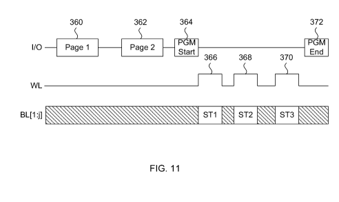
11, which shows a general sequence diagram of the operation of the memory
device of
-16-
CA 02802219 2012-12-11
WO 2012/009812 PCT/CA2011/050442
the present embodiments. Figure 11 shows signal traces for the memory device
input
output port I/O, a selected wordline of the memory device WL, and of bit lines
BL[1:j]. The
method of Figure 10 starts at step 350 where a first page of data is provided
to the
memory device, and is stored in a first page buffer of memory device. As shown
in Figure
11, data Page 1 is received at the I/O port at 360. Shortly thereafter, a
second page of
data is provided to the memory device at step 352, which is stored in a second
page
buffer of memory device. As shown in Figure 11, data Page 2 is received at the
I/O port at
362. From this point on, steps 302 to 312 are the same as those shown and
described for
Figure 9. Multipage programming is initiated at step 302, via a multipage
program start
command 364 of Figure 11.
[0043] Once multipage programming is initiated within the memory device, the
selected wordline WL is driven at 3 different time periods each with a
predetermined
programming profile. It should be noted that only 3 of the 4 possible states
per cell are
programmed since one of the states is the default erased state. In Figure 11,
the 3 time
periods are shown by the wordline WL being driven to the high logic level at
366, 368 and
370. It should be noted that in the memory device, the wordline WL can be
driven to
different voltage levels for a specific amount of time during each time
period. In one
embodiment, program verify operations can be executed after each time period
for
validating the threshold voltage that was just programmed to the cells. Figure
11 shows
that the bit lines are biased during time periods 366, 368 and 370 for
programming states
1, 2 and 3 respectively. In the present example embodiment, at the end of time
period
366 certain memory cells will have a final threshold voltage corresponding to
state
1(ST1), at the end of time period 368 certain memory cells will have a final
threshold
voltage corresponding to state two (ST2), and at the end of time period 370
certain
memory cells will have a final threshold voltage corresponding to state 3
(ST3). After time
period 370 has lapsed, steps 304 to 312 are executed and the program cycle
ends at 372
in Figure 11 with the memory device reporting to the memory controller via its
status
registers if the multipage programming operation was successful or not.
[0044] Figure 12A is a sequence diagram showing an example command and
data input sequence for a flash memory device according to the present
embodiments.
New Figure 11 A shows signal traces for the memory device input/output port
I/O and a
ready/busy signal R/B# provided by the memory device. The present example
command
and data input sequence is illustrated for a two-page multipage program
operation. The
commands shown in Figure 12A can be provided in any format that is understood
by the
memory device to have the same function as presently described. Starting from
the left
-17-
CA 02802219 2012-12-11
WO 2012/009812 PCT/CA2011/050442
side of new Figure 11 A, the first command to be received is a data load
command 380,
followed by input data, which includes address information 382 and write data
384.
Address information 382 can include bank, row and column address information,
and
write data 384 is a page of data to be programmed to the memory device. A data
end
command 386 is received to indicate the end of the input data. Up to this
point in time, the
R/B# signal is at the high logic level to indicate that the memory device is
in a ready state
and is available to receive the information appearing on the I/O port. After
the data end
command 386 is received, the memory device may enter a busy state where R/B#
falls to
the low logic level for a very short period of time.
[0045] After R/B# rises to the high logic level, the memory controller can
resume
the multipage programming operation by issuing another data load command 388.
Following is a second set of input data including address information 390 and
write data
392. The address information can include the same column address as in address
information 382, but would have a different row address to designate the write
data as the
second logical page. A final data end and multi-page program command 394 is
received
to indicate the end of the write data 392, and to initiate internal multipage
programming
operations of the memory device. Command 394 can be provided as a separate
data end
command, and a separate multipage program command. Thereafter, R/B# falls to
the low
logic level for a period of time required to program the to logical pages to a
physical page
of the memory device.
[0046] Figure 12B shows a variation of the command and data input sequence of
Figure 12A. In this embodiment, the memory device may not have the short busy
period
between command 386 and 388, and receipt of the data end command 386 is not
required. Therefore the second data load command 388 can also serve as the
data end
command for write data 384. Figure 12A and Figure 12B are example command and
data
input sequences for controlling a memory device capable of multipage
programming,
however any command and data input sequence which results in loading of the
page
buffers of the memory device followed by internal multipage programming can be
used.
[0047] As previously discussed, the memory cells connected to all bit lines
are
programmed to their respective logic states in one programming cycle, thereby
avoiding
the need to read out the page of data previously programmed in a previous
programming
cycle, before initiating a subsequent programming cycle for programming both
pages of
data to the same physical page. Following is a discussion of different
techniques for
programming all possible logic states to the memory cells of a memory device.
-18-
CA 02802219 2012-12-11
WO 2012/009812 PCT/CA2011/050442
[0048] Figure 13 is a flow chart outlining a method for programming multiple
pages of data to one physical page of memory, according to a present
embodiment. It is
assumed that all the pages to be programmed in the multipage programming
operation
have been loaded into the page buffers of the memory device. Furthermore, it
is assumed
that all memory cells are currently in the erased state, and can have for
example a
negative threshold voltage. This erased state is referred to as STO, as shown
in Figure
14B. The different states are to be programmed in an order of increasing
corresponding
threshold voltages. In the present example a first program state ST1 is
programmed,
followed by a second program state ST2, and then by a third program state ST3.
The
multi-page programming method of Figure 13 is described with reference to an
example 2
bit per cell programming scenario. Reference is made to Figure 14A which is a
timing
diagram showing signal traces for a selected wordline WL and four bitlines
BL1, BL2, BL3
and BL4, and to Figure 14B that illustrates programming of threshold voltages
for cells
connected to the selected wordline and each of bitlines BL1, BL2, BL3 and BL4.
In this
scenario, the memory cells connected to BL1, BL2, BL3 and BL4 are to store
threshold
voltages corresponding to ST2, ST1, ST3 and ST2, respectively.
[0049] The method begins at step 400 where bitline biasing for the first state
ST1
(where n=1) to be programmed is determined for all the bitlines. More
specifically, the
bitlines are biased either to a first voltage sufficient for enabling
programming such as a
low logic level (VSS), or to a second voltage sufficient for inhibiting
programming of the
memory cell such as a high logic level (VDD). At the time preceding tj in
Figure 14A, the
selected wordline WL is maintained at an inactive level of VSS. Proceeding to
step 402,
the bitlines are biased for programming or inhibiting programming of the first
program
state (ST1) n=1. Because states ST2 and ST3 have final threshold voltages
greater than
the threshold voltage corresponding to state ST1, bitlines BL1, BL3 and BL4
are biased to
VSS along with BL2. Following at step 404 the selected wordline is driven to
program any
flash memory cells connected to a bitline biased to the low logic level. In
Figure 14A, the
selected wordline WL is driven to a representative high logic level at time
tj. This
representative high logic level is used to show application of a programming
profile
effective for programming the threshold voltage corresponding to the n=1
program state.
In actual use, the wordline could be driven to a high voltage level, or
stepped in
accordance with known wordline programming control schemes. Programming for
state
n=1 will end at a time determined by the specific programming profile for
state n=1, at
which time the selected wordline is reset at step 406.
-19-
CA 02802219 2012-12-11
WO 2012/009812 PCT/CA2011/050442
[0050] In Figure 14A, resetting WL to VSS occurs at time t2. The time period
bound by tj and t2 is the first iteration of the program cycle. While not
shown in Figure 13,
a program verify operation is executed to validate the threshold voltage of
ST1 stored in
the memory cell after time t2. For the purposes of this example, it is assumed
that all the
memory cells are successfully programmed with the proper threshold voltages.
Ideally,
the flash memory cell connected to BL2 will have a final threshold voltage
corresponding
to ST1, as shown in Figure 14B. However, the memory cells connected to BL1,
BL3 and
BL4 should now have intermediate threshold voltages corresponding to ST1, as
shown by
the dashed threshold voltage distribution curves in Figure 14B, as these are
not the final
threshold voltages for the cells connected to these bitlines. Returning to
Figure 13, a
determination is made at step 408 if the programmed state is the last state to
be
programmed. If so, then the method ends at step 410. Otherwise, there are more
states
to be programmed, and the method proceeds to step 412 where n is incremented
(n=2) to
indicate the next state to be programmed in a subsequent iteration. The method
then
returns to step 400 where the bitline biasing for step ST2 is determined.
Because the
memory cell connected to BL2 is intended to have a final state of ST1, the
program verify
circuits will inhibit BL2 from receiving the VSS voltage for enabling
programming for all
subsequent programming iterations in the present programming cycle.
[0051] Steps 402, 404 and 406 are repeated in a second iteration to program
the
second program state n=2, corresponding to ST2. In the example of Figure 14A,
this
second iteration occurs between times t3 and t4 where BL1, BL3 and BL4 are
biased for
programming. As shown in Figure 14B, the flash memory cells connected to BL1
and BL4
have final threshold voltages corresponding to ST2, while the memory cell
connected to
BL3 now has an intermediate threshold voltage corresponding to ST2. After the
wordline
is reset in step 406, BL1 and BL4 are inhibited from receiving any further VSS
voltage in
any subsequent programming iteration since the memory cells connected to these
two
bitlines are intended to have a final state of ST2.
[0052] Since the program state corresponding to ST3 is yet to be programmed, a
third iteration of steps 400, 402, 404 and 406 are repeated in a third
iteration to program
the third program state n=3, corresponding to ST3. In the example of Figure
14A, this
third iteration occurs between times t5 and t6 where BL3 is biased to VSS for
programming As shown in Figure 14B, the flash memory cell connected to BL3 has
a final
threshold voltage corresponding to ST3. Since program state n=3 is the last
state to be
programmed, the programming cycle will end at step 410.
-20-
CA 02802219 2012-12-11
WO 2012/009812 PCT/CA2011/050442
[0053] Therefore in the above described multipage programming method, any
memory cell having a final threshold voltage greater than the current
threshold voltage
being programmed will have its threshold voltage increased at the same time.
Therefore,
based on the manufacturing process, device geometries and desired threshold
voltages
for each state, each wordline programming profile for a particular program
iteration is
engineered to have a cumulative effect for changing the threshold voltage of a
memory
cell to a desired threshold voltage. In the embodiment of Figure 14A by
example, the
program iteration between time t3 and time t4 for BL1 shifts the threshold
voltage of the
memory cell from intermediate state ST1 to the threshold voltage corresponding
to the
final state ST2.
[0054] According to an alternate embodiment, each wordline programming profile
can be engineered to shift or change an erase threshold voltage directly to a
threshold
voltage corresponding to a final state. This embodiment is illustrated in
Figure 15A and
Figure 15B. It is assumed that the same states are being programmed to the
memory
cells connected to BL1, BL2, BL3 and BL4 as in the example shown in Figure 14A
and
Figure 14B. In the present embodiment of Figure 15A and Figure 15B, the
bitline is only
biased to a voltage level for enabling programming for the duration of one
program
iteration where the wordline is driven with a specific programming profile. As
shown in
Figure 15A, BL1 is driven to the low logic level of VSS just before the
wordline is driven at
time t3, and is then driven back to the high logic level of VDD just after the
wordline is de-
asserted at time t4. As shown in Figure 15B, erase threshold voltage of the
memory cell
connected to bitline BL1 is shifted directly to a threshold voltage
corresponding to state
ST2. Similar biasing sequences for bitline BL2, BL3 and BL4 are shown in
Figure 15A for
programming states ST1, ST2 and ST3 respectively. Accordingly, there are three
specific
wordline programming profiles each effective for shifting the erase threshold
voltage to
each of the threshold voltages corresponding to ST1, ST2 and ST3, and the
bitlines are
biased to enable programming for that specific state while being biased for
inhibiting
programming for all other states.
[0055] Timing and voltage level control of the selected wordline for the
various
programming profiles for the multipage programming embodiments of Figure 14A
and
Figure 15A is provided by control circuit 108 of Figure 8, via high voltage
generator 106
and row circuits 104. In both embodiments, the timing for biasing the bitlines
is controlled
by control circuit 108 and in response to the pages of data stored in the page
buffers.
[0056] The biasing of each of the bit lines for programming data or inhibiting
programming of data in the multipage programming schemes shown in Figure 14A
and
-21 -
CA 02802219 2012-12-11
WO 2012/009812 PCT/CA2011/050442
Figure 15A, can be done in response to the logic states of the bits stored in
the page
buffers 112 and 114 of Figure 8. For example, a specific logic state of a pair
of bits stored
in page buffers 112 and 114 corresponding to a bitline indicates that the
bitline is to be
biased to a voltage level effective for enabling programming of a selected
memory cell.
With reference to Figure 4 by example, State 1, State 2 and State 3 each have
a pair of
bits where at least one of the bits is a logic 0. Therefore in this example,
the presence of
at least one logic 0 bit of a pair of bits corresponding to one bitline can be
detected for
biasing the bitline to a voltage level effective for enabling programming.
Otherwise, if both
pairs of bits are logic 1, then the bitline is biased to a voltage level
effective for inhibiting
programming of a selected memory cell connected to that bitline. It is noted
that State 0
of Figure 4 has both bits at a logic one. Since State 0 is the default erased
state, any
bitline having binary values "11" associated with it is biased for inhibiting
programming.
[0057] Therefore, the example binary values assigned to State 0, State 1,
State 2
and State 3 of Figure 4 can be advantageously used for controlling the
bitlines in the
multipage programming scheme shown in Figure 14A. More specifically, certain
bit lines
are biased to a high logic level after each programming iteration for
inhibiting further
programming in subsequent programming iterations, if the final desired program
state for
that bitline has been verified after a specific programming iteration. On the
other hand, if
this specific programming iteration results in successful programming of an
intermediate
state, then the bitline should remain biased for further programming in a
subsequent
programming iteration. This can be achieved by toggling the logic states of
the pairs of
bits corresponding to each bitline to different values.
[0058] In one example, the logic states of a pair of bits can be toggled to
the
binary value of "11" which indicates that the final state has been programmed,
or to a
binary value including at least one logic 0 which indicates that an
intermediate state has
been programmed. Data state transition rules can implemented to ensure that
the data
transitions from an original data state to one or more intermediate states,
and finally to a
final state.
[0059] Using the example binary value assignments shown in Figure 4, and the
presence of at least one logic 0 bit in a pair of bits to enable programming,
the following
example data transition rules can be developed:
[0060] (1) "10" to "11"
[0061] (2) "00" to "10"
[0062] (3) "01 " to "00"
-22-
CA 02802219 2012-12-11
WO 2012/009812 PCT/CA2011/050442
[0063] Table 1 below illustrates an example application of these data
transition
rules for bitlines, BL1, BL2 and BL3 shown in Figure 14A. In Table 1, 3
program iterations
are shown as "PGM 1", "PGM 2" and "PGM 3". Each program iteration starts with
the
initial binary values "Initial" stored in the data buffers corresponding to
the respective
bitline, which are toggled to new binary values "New" after successful program
verification.
[0064] Table 1
PGM 1 PGM 2 PGM 3
Initial New Initial New Initial New
BL1 1100" 1110" 1110" "11" - -
BL2 1110" "11" - - - -
BL3 "01" "00" "00" "10" "10" "11"
[0065] Figure 16 is a functional block diagram of the bitline access circuitry
110
shown in Figure 8, according to a present embodiment. Figure 16 is intended to
illustrate
the general principle for biasing bitlines for enabling or inhibiting
programming of the
selected memory cell in response to the data stored in the page buffers
associated with
or corresponding to a particular bitline, and it is assumed that other
circuits, such as
bitline sense amplifiers and program verify circuits are present to enable
proper
operation. Such other circuits are not shown in order to simplify the
schematic. Only the
circuits associated with a first bitline BL[1] and the last bitline BL[j] are
shown in Figure
16. The bitlines are biased by the bitline access circuitry 110 in
coordination with the
wordlines being driven at the different time intervals. Page buffer 112
includes a plurality
of data storage circuits 500, each for storing 1 bit of a first page of data.
Page buffer 114
includes a plurality of data storage circuits 502 each for storing 1 bit of a
second page of
data. Each pairing of data storage circuits 500 and 502 connected to AND logic
gate 504
are associated with a respective bitline.
[0066] In addition to storing bits of the first page of data and the second
page of
data, bitline access circuitry 110 includes data decoding circuitry for
biasing each bitline
to either a program inhibit voltage or a program enable voltage in response to
the specific
logic states of the bits from both pages of data corresponding to the bitline.
The data
decoding circuitry for each bitline includes an AND logic gate 504 and a data
verify
decoder 506. Prior initiation of a program iteration, the AND logic gate 504
receives the
logic states stored in data storage circuits 500 and 502, and biases the
bitline in response
to the logical AND operation. In the presently described examples, a bitline
is biased to
VSS when at least one of the data storage circuits 500 and 502 stores a logic
0.
-23-
CA 02802219 2012-12-11
WO 2012/009812 PCT/CA2011/050442
[0067] The data verify decoder 506 includes logic circuitry for decoding the
logic
states stored in data storage circuits 500 and 502, and for selectively
inverting either
stored logic state such that data storage circuits 500 502 store new binary
values in
response to a detected condition of the bitline indicative of successful
programming. This
can be considered program verify circuitry. This selective inversion of either
stored logic
state in data storage circuits 500 and 502 is done in accordance with the
predetermined
data transition rules. In the present embodiment, inversion of the data
storage circuits 500
and 502 is executed in response to successful program verification of a
completed
program iteration. If the memory cell has not been sufficiently programmed to
have the
desired threshold voltage, then programming is repeated. In the present
example, a
successfully programmed memory cell for any program state forms a current path
to VSS,
thereby discharging a bitline pre-charged to VDD to VSS during the program
verify
operation. Otherwise, the bitline remains substantially at the pre-charged VDD
level to
indicate that a repeated programming iteration is required for the memory cell
connected
to that bitline. Therefore in the present embodiments, selective data
inversion in
accordance with the data transition rules is executed when the bitline is at
VSS a program
verify operation. Otherwise, no selective data inversion is executed.
[0068] Figure 17 shows further details of the data verify decoder 506 and its
interconnections to data storage circuits 500 and 502, according to present
embodiment.
Data storage circuit 500 includes a logic 0 inversion circuit 600 and a logic
1 inversion
circuit 602. Data storage circuit 502 includes a logic 0 inversion circuit 604
and a logic 1
inversion circuit 606, both of which are the same as circuits 600 and 602
respectively.
The logic 0 inversion circuit 600 will invert any logic 0 state stored in data
storage circuit
500 to a logic 1 state, in response to a decoded data signal received from
data verify
decoder 506. The logic 1 inversion circuit 602 will invert any logic 1 state
stored in data
storage circuit 500 to a logic 0 state, in response to a decoded data signal
received from
data verify decoder 506. Inversion circuits 604 and 606 perform the same
function as
described above for inversion circuits 600 and 602. As shown in Figure 17,
inversion
circuits 600, 602, 604 and 606 receive different decoded data signals.
[0069] The data verify decoder 506 includes AND logic gates 604, 606 and 608.
Each AND logic gate has a first input which receives the stored logic state
from data
storage circuit 500, and a second input which receives the stored logic state
from data
storage circuit 502. It should be noted that each AND logic gate has a
different
combination of inverted and non-inverted first and second inputs, and the
output of each
AND logic gate is provided to specific inversion circuits (600, 602 , 604 and
606). This
-24-
CA 02802219 2012-12-11
WO 2012/009812 PCT/CA2011/050442
configuration of the different combinations of inverted and non-inverted first
and second
inputs is a specific example of an implementation of the previously described
data
transition rules. While not shown, each bitline includes detection circuitry
for detecting the
low voltage level of the bitline during program verification, and enabling the
data verify
decoder 506. Otherwise, if a high voltage level of the bitline is detected,
then
programming was not successful and the data verify decoder 506 is disabled to
prevent
inversion circuits 600, 602, 604 and 606 from operating.
[0070] An example operation of the circuits of Figure 17 now follows using the
previously described example scenario of BL3 of Table 1 where the initial
binary value of
"01" is stored in data storage circuits 500 and 502. Accordingly, it should be
understood
that data storage circuit 500 stores in logic 0 while data storage circuit 502
stores a logic
1. Following the first program iteration PGM 1 and assuming that program
verification is
successful, the initial binary value of "01" causes AND gate 612 to output a
logic 1 to logic
1 inversion circuit 606. In response, logic 1 inversion circuit 606 toggles
the data storage
circuit 502 and the initially stored logic 1 is changed to a logic 0. Logic 0
inversion circuit
600 received a logic 0 from AND gate 608 and therefore does not toggle data
storage
circuit 500. Accordingly, the new binary value is "00" store in data storage
circuits 500
and 502, and the corresponding bitline remains biased to enable programming
for the
subsequent program iteration PGM 2. After successful program verification of
PGM 2, the
data verify decoder 506 can decode the "00" binary values from data storage
circuits 500
and 502. Now, AND logic gate 608 outputs a logic 1 to logic 0 inversion
circuit 600, which
toggles the data storage circuit to change the stored logic 0 to a logic 1.
The outputs of
AND logic gates 610 and 612 are at the inactive logic 0 state, therefore no
changes are
made to data storage circuit 502.
[0071] Now the new binary value of "10" is stored in data storage circuits 500
and
502, and the corresponding bitline remains biased to enable programming for
the
subsequent program iteration PGM 3. After successful program verification of
PGM 3, the
data verify decoder 506 can decode the "10" binary values from data storage
circuits 500
and 502. AND logic gate 604 outputs a logic 1 to logic 0 inversion circuit
604, which
toggles the data storage circuit 502 to change the stored logic 0 to a logic
1. Now both
data storage circuits 500 and 502 store a logic 1, and the bitline is biased
to VDD for
inhibiting programming. The presently shown example data verify decoder 506
and its
connections to the inversion circuits ensures that for any initial
programmable state of
Figure 4 stored in the data storage circuits 500 and 502 will be transitioned
to the next
intermediate or final state according to the data transition rules.
-25-
CA 02802219 2012-12-11
WO 2012/009812 PCT/CA2011/050442
[0072] The presently described data transition rules and example circuit
embodiments shown in Figures 16 and 17, are presented to illustrate the
principle behind
biasing the bitlines based on a specific binary value assignment for possible
storage
states, such as for the binary value assignments shown in Figure 4. An
assignment of
different binary values for these 4 states can be used, and a different set of
data transition
rules can be developed. Accordingly, the configuration of data verify decoder
506 and its
connection to the inversion circuits can be adapted to accommodate such an
alternate
binary value assignment and data transition rules. The presently described
embodiments
are directed to a 2 bits per cell configuration, but can be easily scaled for
3 bit per cell or
more configurations based on the presently described principles. Other circuit
techniques
can be used for achieving the same desired result. Furthermore, the present
examples
described how a logic "0" is used to indicate further biasing of a bitline for
enabling
programming, but alternate embodiments can use a logic "1" instead.
[0073] Therefore, the multipage programming circuits and methods described in
the previous embodiments reduces the total program time relative to prior
techniques
where multiple program cycles are required for programming each logical page
of data to
a physical page. This is due to the fact that timing overhead typically
required for
programming different logical pages in different programming cycles is
eliminated in the
present multipage programming embodiments because all the logical pages are
programmed within one programming cycle. Furthermore, there is a reduction in
programming stress of the flash memory cells when compared to using separate
programming cycles for programming each logical page. Additionally, this power
is
required for programming when using the presently described multipage
programming
embodiments relative to the prior art programming techniques.
[0074] The previously described embodiments can be further improved for
reducing the overall time required for programming all states in one
programming cycle.
In the previously described embodiment of Figure 11 by example, multiple
programming
iterations are sequentially executed for programming each state to the
selected cells for
that particular iteration. More specifically, one programming cycle for
programming
multiple states or pages to memory cells involves sequential application of
different bitline
voltages and driving the selected wordline with a particular programming
profile for a
specific state/threshold voltage to be programmed. Therefore the total time
for the
programming cycle is the sum of the time required for each programming
iteration.
According to a present alternate embodiment, the programming cycle time can be
significantly reduced by programming all possible states to the cells in a
single
-26-
CA 02802219 2012-12-11
WO 2012/009812 PCT/CA2011/050442
programming iteration. In otherwords, instead of sequential programming
iterations for
programming each state, all the states are programmed in parallel when the
selected
wordline is driven with a programming profile. This is referred to as parallel
multi-state
programming
[0075] Figure 18A is a sequence diagram showing an example two-page parallel
multi-state program operation of a flash memory device, according to a present
embodiment. This sequence diagram is similar to the one shown in Figure 11, in
that data
Page 1 is received at the I/O port at 360 and data Page 2 is received at the
I/O port at
362. Multipage programming is initiated via a multipage program start command
364, as
in Figure 11, as is the indication to the memory controller that the program
cycle has
ended at 372 with the memory device reporting to the memory controller via its
status
registers if the multipage programming operation was successful or not.
However, instead
of the 3 time periods 366, 368 and 370 required for programming all the
states, only one
single time period 700 is required. During this time period 700 where the
selected
wordline is driven with a predetermined programming profile, the bitlines
BL[1:j] are
biased to specific voltage levels for programming threshold voltages
corresponding to
different states, where the voltage levels are calibrated for a particular
manufacturing
process. It is noted that the programming profile of the wordline is optimized
for effective
programming of the threshold voltages for the particular manufacturing
process.
[0076] As shown in Figure 18A, states ST1, ST2 and ST3 are programmed at the
same time to the memory cells in response to specific bitline voltage levels
while the
wordline is driven during time period 700. Figure 18B is a threshold voltage
distribution
graph showing threshold voltages of 4 flash cells programmed in Figure 18A
connected to
bit lines BL1, BL2, BL3 and BL4. As shown in Figure 18B, the memory cells are
shifted
from STO to their respective final programmed threshold voltages corresponding
to ST1,
ST2 and ST3 during time period 700.
[0077] Figure 19A and Figure 20A are alternate sequence diagrams showing
example two-page mixed sequential and parallel multi-page program operations
of a flash
memory device. In these alternate embodiments, multiple program iterations are
used,
where a subset of the possible states to be programmed are programmed in
parallel in
one iteration while a remaining state or states are programmed in a second
iteration.
[0078] In Figure 19A, reference numbers 360, 362, 364 and 372 are the same as
previously described for Figure 18A and Figure 11. In this alternate
embodiment, one
state ST1 is programmed at time period 702, followed sequentially with
parallel multi-
state programming of states ST2 and ST3 at time period 704. It is noted that
after the first
-27-
CA 02802219 2012-12-11
WO 2012/009812 PCT/CA2011/050442
programming iteration occurring at time period 702, the memory cells
designated for
storing states ST2 and ST3 will have the same threshold voltage corresponding
to state
ST1. In the following time period 704, the cells having the threshold voltage
corresponding to ST1 are further adjusted to correspond to states ST2 and ST3.
As
shown in the threshold voltage distribution graph of Figure 19B, the memory
cells starting
with the erased threshold voltage corresponding to the state of STO are
shifted to the
programmed threshold voltage corresponding to ST1 in time period 702. In time
period
704, the memory cells connected to bit lines BL1, BL3 and BL4 have their
intermediate
threshold voltages corresponding to ST1 shifted to the final threshold
voltages
corresponding to ST2 and ST3.
[0079] In the embodiment of Figure 20A, parallel multi-state programming of
states ST1 and ST2 occurs at time period 706, followed sequentially with
programming of
remaining state ST3 at time period 708. It is noted that after the first
programming
iteration occurring at time period 706, the memory cells designated for
storing state ST3
will have the same threshold voltage corresponding to the state having the
higher
threshold voltage, which in this example is state ST2. In the following time
period 708, the
cells having the threshold voltage corresponding to ST2 are further adjusted
to
correspond to state ST3. As shown in the threshold voltage distribution graph
of Figure
20B, the memory cell connected to BL2 has its erased threshold voltage shifted
to the
threshold voltage corresponding to ST1 in time period 706. Also occurring in
time period
706, the memory cells connected to BL1, BL3 and BL4 have their erased
threshold
voltages shifted to the threshold voltage corresponding to ST2, including the
memory cell
connected to BL3. In time period 708, the memory cell connected to bit line
BL3 has its
intermediate threshold voltage corresponding to ST2 shifted to the final
threshold voltage
corresponding to ST3.
[0080] In both the alternate embodiments shown in Figures 19A, 19B, 20A and
20B, at least two states are programmed in parallel. It should be noted that
these
embodiments are non-limiting, as alternate embodiments can include having a
first
program iteration to program at least 2 states in parallel, followed by a
second program
iteration to program at least another 2 states in parallel. Furthermore,
combinations of
parallel multi-state programming iterations and single state programming
iterations can be
used.
[0081] For the embodiments shown in Figure 18A, Figure 19A and Figure 20A,
the command and data input sequences shown in Figure 12A and Figure 12B can be
used for loading the memory device with pages of data, and to initiate a multi-
state
-28-
CA 02802219 2012-12-11
WO 2012/009812 PCT/CA2011/050442
parallel programming operation or one of the two mixed sequential and parallel
multi-state
program operations.
[0082] The presently disclosed embodiments of parallel multi-state programming
are achieved by biasing the bitlines to specific voltages, referred to as
bitline voltage
modulation. As previously discussed, a memory cell connected to a bitline is
either
inhibited from being programmed or enabled for programming via the selected
wordline,
depending on the logic level the bitline is biased, or set to. Commonly owned
U.S. Patent
No. 7,511,996, incorporated herein by reference, describes embodiments for
inhibiting
programming of a memory cell, in which memory cells selected for programming
have
their bit lines biased to a program voltage such as OV for example, and memory
cells not
to be programmed have their bitlines biased to a program inhibit voltage such
as VCC for
example. A description of one such embodiment described in U.S. Patent No.
7,511,996
is first provided in order to facilitate an understanding of how a program
inhibit voltage
applied to a bitline can inhibit programming of a selected memory cell.
[0083] Figure 21 is a flow chart illustrating an embodiment of a program
inhibit method of
U.S. Patent No. 7,511,996. In the present discussion, upper wordlines refer to
those
wordlines and memory cells between the selected memory cell and the bitline,
while
lower wordlines refer to those wordlines and memory cells between the selected
memory
cell and the sourceline. The program inhibit method of Figure 21 begins at
step 800,
where the bitlines are biased with an inhibit voltage or a program voltage. In
the presently
described example, it is presumed that the bitline is driven to an inhibit
voltage of VCC. At
step 802, the selected wordline and the upper wordlines are driven to a first
pass voltage.
This first pass voltage is high enough to turn on each memory cell
corresponding to an
upper wordline, regardless of its programmed or unprogrammed state.
Concurrently with
step 802, the lower wordlines are driven to a second pass voltage at step 804.
According
to embodiments of the present method, the first pass voltage and the second
pass
voltage can be identical to each other, or the second pass voltage can be
lower than the
first pass voltage. The selected wordline is then driven to a programming
voltage at step
806, followed by an isolation operation at step 808 for decoupling the
selected memory
cell from the unselected memory cells of the NAND string.
[0084] Figure 22A is a simplified cross sectional view of a NAND string 900,
which should
be well known to persons skilled in the art. NAND string 900 includes memory
cells 902
having gates connected to wordlines WLO to WL31, a string select transistor
904 for
coupling the NAND string 900 to a bitline 906, and a ground select transistor
908 for
coupling the NAND string 900 to a source line 910. The NAND string 900 is
formed within
-29-
CA 02802219 2012-12-11
WO 2012/009812 PCT/CA2011/050442
a PP-Well, which is itself formed within an N-Well of the P-substrate. The
source/drain
regions of the NAND string memory cell transistors are n+ diffusion regions.
[0085] Figure 22A includes annotations to show relative voltage levels applied
to specific
wordlines, according to an embodiment of the present invention. It is noted
that the
physical NAND string remains unchanged from the prior art. In the example
shown in
Figure 22A, it is assumed that the memory cell connected to WL29 is selected
for
programming, and the data to be programmed is the logic "1" state. Since the
erased
state is a logic "'I", programming is to be inhibited. Figure 22B is a
sequence diagram
further illustrating the sequence of the voltages being applied in Figure 22A.
[0086] Time period T1 is an initial state, where the gates of all the memory
cells 902,
signal SSL, and signal GSL are biased to OV, while the bitline voltages for
programming
memory cells and for inhibiting programming of memory cells are applied. CSL
can be
biased to either OV or VCC, but can be preferably biased to VCC in the present
example
to minimize leakage. In the present example, bitline 906 is biased to VCC to
inhibit
programming. At time period T2, signal SSL is biased to VCC for coupling the
bitline
voltage to NAND string 900. In NAND string 900 shown in Figure 22A, string
select
transistor 904 electrically turns off because its drain terminal connected to
the bitline 906
and its gate are both biased to VCC. More specifically, string select
transistor 904 will turn
off once its source rises to about VCC minus a threshold voltage of the
transistor. During
time period T3, all the wordlines (upper, lower and selected wordlines) are
driven to a
pass voltage V2, where V2 is selected to be higher than VCC. This has the
effect of
boosting the entire channel of NAND string 900 to the primary boosted voltage.
At the
beginning of time period T4, the selected wordline WL29 is raised to the
programming
voltage V1 while the adjacent wordlines WL28 and WL30 are reduced to a
decoupling
voltage V3. These correspond to steps 104 and 106 respectively in Figure 5.
The voltage
level of V1 is set to be higher than V2, and the voltage level of V3 is set to
be lower than
V1 and V2.
[0087] A further advantage of reducing the wordline voltage of WL28 and WL30
to V3 is
to compensate for capacitive coupling between the control gate connected to
WL29 and
the floating gates coupled to WL28 and WI-30. As WL29 is driven to V1, the
capacitive
coupling effect can increase the floating gate voltage, thereby increasing the
probability of
pass disturbance in the memory cells immediately adjacent to the selected
memory cell.
Therefore, the reduction of the wordline voltage to V3 will reduce the
floating gate
voltage.
-30-
CA 02802219 2012-12-11
WO 2012/009812 PCT/CA2011/050442
[0088] In the embodiment shown in Figure 22A the voltage levels of V1, V2 and
V3 can
be selected according to the following criteria. V1 should be a voltage level
high enough
to promote F-N tunneling in a memory cell coupled to a bitline biased to OV.
The voltage
level of V2 should be selected to satisfy the following three criteria. First,
V2 should be
high enough to ensure that the channels of unselected cells are made to be
conductive.
Second, when the voltage V2 falls down to the voltage V3 for WL28 and WL30
during
time period T4, the memory cells connected to WL28 and WL30 are turned off and
remain turned-off during time period T4. This is the local decoupling effect
that is
achieved. Third, when the selected wordline WL29 rises to the program voltage
V1 from
voltage V2, the channel of the selected cell can be boosted to a desired
voltage, namely
to the secondary boosted voltage level. V3 should be a voltage level high
enough to pass
a OV bitline voltage through unselected cells to the drain of a selected cell,
while being
sufficiently low to substantially turn off the channels of the memory cells
(connected to
WL28 and WL30) immediately adjacent the selected cell (connected to WL29).
[0089] The currently described program inhibit scheme can be modified for the
presently described parallel multi-state programming embodiments, by varying
the
voltage applied to the bitlines prior to driving the wordlines during the
program iteration. In
the previously described program inhibit embodiment, the application of a
program inhibit
voltage of VCC minimizes the electric field strength between the selected word
line driven
to V1 and the channel of the selected cell when the bit line is biased to VCC.
According to
the present embodiments, by biasing the bitline to a voltage between VCC and
VSS, this
electrical field strength is increased relative to the full VCC inhibit
situation, thereby
allowing the threshold voltage of the cell to be shifted positively. However,
the amount by
which the threshold voltage shifts will be less than if the bitline was biased
to VSS.
Therefore, the cell is partially inhibited from being fully programmed.
[0090] Figure 23 is a circuit schematic of four flash memory NAND cell strings
showing example voltage biasing of the bitlines for a parallel multi-state
programming
embodiment for a two-bit per cell storage scheme. The elements of the NAND
cell strings
shown in Figure 23 have been previously described for the NAND cell string
previously
shown in Figure 22A, and therefore use the same reference numbers to designate
the
same elements. Each of the NAND cell strings is connected to a respective
bitline, BLO,
BL1, BL2 and BL3. In the presently shown example, BLO is biased to VCC, BL1 is
biased
to VBL1, BL2 is biased to VBL3 and BL3 is biased to VSS. According to the
present
embodiments, all the bitlines are biased with one of these four voltages at
the same time
prior to the wordlines being driven. Then the wordlines are driven for
effecting
-31-
CA 02802219 2012-12-11
WO 2012/009812 PCT/CA2011/050442
programming, such as with the voltages and with the sequence outlined in
Figure 22B for
the described program inhibit scheme. Other program inhibit schemes operating
under
the principle where one voltage is used for inhibiting programming and another
is used for
enabling programming can be adapted for parallel multi-state programming as
taught by
the present embodiments.
[0091] In one example of a two-bit per cell storage scheme, the bitlines can
be
biased to one of the program inhibit voltage of VCC, and program voltages VSS,
VBL1
and VBL2, where VBL1 and VBL2 are both greater than VSS and less than VCC. For
example, VBL1 can be 1 Volt and VBL2 can be 2 Volts. The specific voltage
levels for
VBL1 and VBL2 can be determined based on factors such as the manufacturing
process,
the desired threshold voltage, and the programming profile for the selected
wordline. The
same principles described above can be applied to embodiments where more than
two
bits are to be stored in a memory cell.
[0092] The biasing of the bitlines to a particular voltage level depends on
the logic
states of the bits of the pages of data corresponding to a specific bitline.
Figure 24 is a
block diagram of bitline access circuitry for modulating the bitline voltage
levels for
parallel multi-state programming, according to a present embodiment. Bitline
access
circuitry 1000 includes a page buffer 1002, and at least one multi-page
program buffer
1004. Page buffer 1002 includes a plurality of data storage circuits 1006,
each for storing
1 bit of a first page of data. Page buffer 1004 includes a plurality of data
storage circuits
1008 each for storing 1 bit of a second page of data. Each pairing of data
storage circuits
1006 and 1008 connected to BL modulator 1010 are associated with a respective
bitline.
The data decoding circuitry for each bitline includes BL modulator 1010 and a
data verify
decoder 1012. Elements 1002, 1006, 1008 and 1012 are substantially the same as
elements 112, 114, 504, 502 and 506 shown in Figure 16. The main difference
between
the embodiments of Figure 24 and Figure 16 is BL modulator 1010, which is
responsible
for decoding the data bits of the two pages of data associated with a
particular bitline and
biasing the bitline with a predetermined voltage, and decoding logic of data
verify decoder
1012. Every BL modulator 1010 in the memory array biases its respective
bitline at the
same time, before the program iteration is initiated.
[0093] Figure 25 is a schematic showing the functional blocks of BL modulator
1010. BL modulator 1010 includes a program data decoder 1100 and a bitline
biasing
circuit 1102. The program data decoder 1100 receives a bit of data from a
first page
buffer, referred to as DATA1_[1] and a bit of data from a second page buffer
referred to
as DATA2_[1]. The "DATA1" term indicates that the bit is from the first page
buffer, while
-32-
CA 02802219 2012-12-11
WO 2012/009812 PCT/CA2011/050442
the "DATA2" term indicates that the bit is from the second page buffer. The
"[1]" term
indicates the bit position in the page of data. The program data decoder 1100
decodes
the two bits of data to provide selection signals SO, S1, S2 and S3, where
only one is at
the active logic level for any combination of DATA1_[1] and DATA2_[1]. These
selection
signals are used by bitline biasing circuit 1102 for passing one of
predetermined voltages
VCC, VSS, VBL1 or VBL2 to the bitline BL[1], where VCC>VBL2>VBL1>VSS. In the
present embodiment, each selection signal is mapped to a corresponding
predetermined
voltage. The presently shown embodiment is configured for a two-bit per cell
storage
scheme, which can be scaled for three-bit or more per cell storage schemes.
Therefore,
for each possible combination of DATA1_[1] and DATA2_[1], BL modulator 1010
selects
and biases its bitline to one of predetermined voltages VCC, VSS, VBL1 or
VBL2. The
voltages can be generated by voltage generators.
[0094] Figure 26 is an example circuit schematic illustrating an embodiment of
the
program data decoder 1100 shown in Figure 25. The program data decoder 1100
includes AND logic gates 1200, 1202, 1204 and 1206 each having a first input
and a
second input for receiving page buffer data bits DATA1_[1] and DATA2_[1]. Each
AND
logic gate provides one of selection signals S0, S1, S2 and S3. The first and
second
inputs of the AND logic gates are configured differently so as to ensure that
only one of
the selection signals is driven to the active high logic level for any
combination of
DATA1_[1] and DATA2_[1]. The example logic gate configuration shown in Figure
26 is
one possible configuration which could be used. Different types of logic gates
and input
configurations can be used to obtain the same result shown by the AND logic
gate
configuration shown in Figure 26, which is to select a specific voltage for
application to
the bitline.
[0095] Figure 27 is an example circuit schematic illustrating an embodiment of
the
bitline biasing circuit 1102 shown in Figure 25. Bitline biasing circuit 1102
includes p-
channel transistor 1300, and n-channel transistors 1302, 1304 and 1306. P-
channel
transistor 1300 connects the bitline BL to VCC in response to SO at the high
logic level,
via inverter 1308. N-channel transistor 1302 connects the bitline BL to VBL1
in response
to S1 at the high logic level. N-channel transistor 1304 connects the bitline
BL to VBL2 in
response to S2 at the high logic level. N-channel transistor 1306 connects the
bitline BL
to VSS in response to S3 at the high logic level. Accordingly, through the
selection
signals SO, S1, S2 and S3 provided by program data decoder 1100, one of the
predetermined voltages can be applied to the bitline BL. Different circuit
configurations
-33-
CA 02802219 2012-12-11
WO 2012/009812 PCT/CA2011/050442
can be used to provide the different voltages to the bitline in response to
the selection
signals.
[0096] The circuit embodiment shown in Figure 26 can be used for the parallel
multi-state programming embodiment of Figure 18A, but a modified version of
the circuit
would be used for the mixed sequential and parallel multi-page program
embodiment of
Figure 19A, according to another embodiment. In such an alternate embodiment,
the
logic of program data decoder 1100 would be configured such that in the first
programming iteration for programming state ST1, any memory cell designated
for storing
states ST2 or ST3 will have its respective bit lines biased to the same
bitline voltage
corresponding to ST1, which in the present example is VBL1. This can be done
by
designing logic circuits to achieve this desired result, or alternately, the
transistors 1304
and 1306 of bitline biasing circuit 1102 can be configured to receive VBL1
instead of
VBL2 and VSS respectively, in the first programming iteration. In the next
programming
iteration for programming states ST2 and ST 3 in parallel, the circuit of
Figure 26 can be
used in the previously described manner.
[0097] The mixed sequential and parallel multi-page program embodiment of
Figure 20A would require a similar modification to the logic of program data
decoder
1100. In this case, states ST1 and ST2 are programmed in the first program
iteration.
However, memory cells designated for storing state ST3 should be programmed to
the
intermediate ST2 state in the first program iteration. Therefore, the logic of
program data
decoder 1100 would be configured such that in the first programming iteration
for
programming ST1 and ST2, any memory cell designated for storing state ST3 will
have
its respective bit line biased to the same bitline voltage corresponding to
ST2, which in
the present example is VBL2. Once again logic decoding circuit can be designed
to
achieve this desired result, or alternatively, voltage level switching for
bitline biasing
circuit 1102 can be used.
[0098] The presently described embodiments of the bitline access circuitry
1000
can be used for executing the full parallel multi-state programming embodiment
shown in
Figure 18A where all the possible states are programmed simultaneously. For
the
embodiments of Figure 19A and 20A in which parallel multi-state programming is
executed for some states either before or after another programming iteration
in which
one other state is programmed, the previously described embodiments of the bit
line
access circuitry 1000 can be modified in accordance with the teachings of the
embodiments of Figure 16 and Figure 17. Such modifications adapt the circuits
for
program verification operations unique to the full parallel multi-state
programming
-34-
CA 02802219 2012-12-11
WO 2012/009812 PCT/CA2011/050442
embodiment shown in Figure 18A and to the mixed sequential and parallel multi-
page
program embodiments shown in Figure 19A and Figure 20A. Following is a
discussion of
program verification for the presently described multi-state programming
embodiments.
[0099] In the previously described embodiments where one state is programmed
in each programming iteration, a program verification operation is executed
after each
iteration to ensure that the desired threshold voltage has been properly
programmed to
the memory cells. For the presently described multi-state programming
embodiments, at
least 2 states are programmed simultaneously in one programming iteration.
Therefore, a
new program verify scheme is used for verifying that the threshold voltages
corresponding to the at least 2 states have been programmed to their
respective cells.
[00100] For the embodiment of Figure 18A, although all the states are
programmed
in parallel, program verification is executed sequentially for each state. In
the present
embodiments, when the memory cell connected to a bitline has been verified as
being
successfully programmed, the 2 data buffer bits corresponding to that bitline
are changed
to binary values "11" corresponding to the erased state for inhibiting further
programming.
However, only the data buffer bits for the programmed state being verified
should be
subjected to being toggled to the erased state. Stated differently, the data
buffer bits for
the state not being verified should not be toggled to the erased state during
the program
verify operation for another programmed state. As previously described for the
embodiment of Figure 16, data verify decoder 506 toggles the data buffer
register bits in
the program verify operations. Therefore this circuit should be enabled for
those bit lines
biased during programming to a state for which a program verify operation is
currently
being executed.
[00101] Figure 28 shows a circuit schematic embodiment of a control circuit
for
selectively enabling or disabling a data verify decoder 1012 of the embodiment
of Figure
24, for the multi-state programming embodiment of Figure 18A. Program verify
control
circuit 1400 includes AND logic gates 1402, 1404 and 1406, and an OR logic
gate 1408.
Each AND logic gate has a first input for receiving one of the selection
signals S1, S2 or
S3 provided by program data decoder 1100 shown in Figure 26. Each AND logic
gate has
a second input for receiving verify control signals Verify S1, Verify S2 and
Verify S3
corresponding to selection signals S1, S2 and S3 respectively. The outputs of
AND logic
gates 1402, 1404 and 1406 are logically OR'd together by gate 1408 to provide
an output
for enabling its corresponding data verify decoder 1012. It is noted that no
AND logic gate
is required for state SO, since state SO is the erased state which does not
need to be
-35-
CA 02802219 2012-12-11
WO 2012/009812 PCT/CA2011/050442
program verified. It is assumed that data verify decoder 1012 is configured to
be
responsive to the enable signal from program verify control circuit 1400.
[00102] In operation, program verify control circuit 1400 receives verify
control
signals Verify S1, Verify S2 and Verify S3 at the active high logic level at
different periods,
wherein each period corresponds to a program verification operation for a
specific state.
For example, Verify S1 can be first asserted for verifying state S1, followed
by Verify S2
for verifying state S2. As previously discussed, program data decoder 1100
asserts only
one of selection signals SO, S1, S2 and S3 for any given logic state
combination of
DATA1_[1] and DATA2_[1]. Therefore as each verify control signal Verify S1,
Verify S2
and Verify S3 is asserted for verifying a specific state, only the data verify
decoders 1012
associated with bitlines biased for programming that specific state are
enabled, and all
other data verify decoders 1012 are disabled. The specific logic gate
configuration shown
in Figure 28 is an example of one possible configuration. Alternate logic gate
configurations can be used for enabling data decoder 1012 using the selection
signals in
combination with other control signals in order to achieve the same result.
[00103] Once enabled, the data verify decoders 1012 are configured for
toggling
the pair of data bits of the page buffers corresponding to the bitline, to the
erased state if
programming of that specific state has been deemed to be successful.
Otherwise, the pair
of data bits are unchanged. Hence, unsuccessfully programmed memory cells will
have
their corresponding bit lines biased to the specific voltage level selected by
selection
signals S1, S2 and S3 for re-programming. In the present embodiment, data
verify
decoder 1012 includes logic circuitry configured to toggle the pair of data
bits
corresponding to states ST1, ST2 and ST3 to logic levels corresponding to the
erased
state, such as "11" for example.
[00104] Now that the technique for program verification of the parallel multi-
state
programming embodiment has been described, it is noted that the program verify
technique for the mixed sequential and parallel multi-page programming
embodiments of
Figure 19A and Figure 20A combines the program verify embodiment used in the
sequential programming embodiment of Figure 16 and the program verify
embodiment for
the parallel multi-state programming embodiment of Figure 22.
[00105] Starting with the embodiment of Figure 19A, the first state to be
programmed is state ST1, followed by parallel programming of states ST2 and
ST3.
However, the memory cells designated for storing states ST2 and ST3 are
programmed
in the first programming iteration and therefore store state ST1 as an
intermediate state.
This first programming iteration is similar to the one shown in Figure 14B
where all the
-36-
CA 02802219 2012-12-11
WO 2012/009812 PCT/CA2011/050442
cells are programmed to store state ST1 either as a final state or as an
intermediate
state. Therefore the previously described program verify technique for Figure
14B can be
used. In the next programming iteration, the intermediate states are shifted
to final states.
Therefore as part of a successful program verify operation for the first
programming
iteration, logic circuitry of data verify decoder 1012 is configured to
i)toggle the data bits
corresponding to state ST1 to the erased state; or ii) toggle the data bits
corresponding to
state ST2 to a combination for selecting bitline voltage VBL2; or iii) toggle
the data bits
corresponding to state ST3 to a combination for selecting bitline voltage VSS.
The bit
lines are therefore biased to new voltage levels for the second programming
iteration to
program states ST2 and ST3 in parallel. The program verify technique employed
for the
embodiment of Figure 18A can be used for the second programming iteration.
[00106] For the embodiment of Figure 20A, states ST1 and ST2 are programmed
in parallel in a first programming iteration, followed by programming of state
ST3 in a
second programming iteration. For the first program iteration, the program
verify
technique described for the embodiment of Figure 18A can be used. As part of a
successful program verify operation for the first programming iteration, the
logic circuitry
of data verify decoder 1012 is configured to i) toggle the data bits
corresponding to state
ST1 or ST2 to the erased state; or ii) toggle the data bits corresponding to
state ST3 to a
combination for selecting bitline voltage VSS. The bit lines are therefore
biased to new
voltage levels for the second programming iteration to program state ST3. The
program
verify technique employed for the embodiment of Figure 14B can be used for the
second
programming iteration.
[00107] The previously disclosed and described circuits and logic
configurations
are presented as examples of embodiments which could be used for implementing
the
different multi-state programming embodiments and corresponding program verify
embodiments. Alternate circuits and logic configurations can be used to obtain
the same
desired result.
[00108] Figure 29 is a flowchart outlining a method for parallel multi-state
programming, according to a present embodiment. This method can be used in
block 302
of the method of Figure 9. The method of Figure 28 starts at 1500 by decoding
the bits of
the pages of data corresponding to each bitline, as described in the
previously disclosed
circuit embodiments, for determining the states to program. At 1502, the bit
lines are
biased to voltage levels corresponding to each of the different states to
program. Once
the bit lines are biased to their respective voltage levels, a selected word
line is driven at
1504 with a programming profile for simultaneous programming of the different
states to
-37-
CA 02802219 2012-12-11
WO 2012/009812 PCT/CA2011/050442
the memory cells, where each different state has a corresponding threshold
voltage.
Once programming is complete, a program verify operation according to the
previously
described embodiments, can be executed at 1506. Elements 1500, 1502, 1504 and
1506
can be used for full parallel multi-state programming of all possible states,
or for parallel
multi-state programming of a subset of all possible states.
[00109] For example, prior to decoding data at 1500 a first programming
iteration
can be executed at 1508 for programming one state with the corresponding
program
verify operation at 1510, thereby leaving the remaining possible states to be
programmed
in parallel at 1500, 1502 and 1504 (the second programming iteration). The
programming
operation executed at 1500, 1502, 1504 and 1506 can be used for programming
all the
possible states except for one state as a first programming iteration. The
remaining state
can be programmed in a second programming iteration 1512, with the
corresponding
program verify operation at 1514. The presently described embodiments are not
limited
to programming one state in a first programming iteration followed by
programming
remaining states in parallel in a second program iteration, or vice versa. In
the situation
where there are many states to be programmed, multiple programming iterations
can be
used where at least 2 states are programmed in each programming iteration.
[00110] In the embodiments described above, the device elements and circuits
are
connected to each other as shown in the figures, for the sake of simplicity.
In practical
applications of the present invention, elements, circuits, etc. may be
connected directly to
each other. As well, elements, circuits etc. may be connected indirectly to
each other
through other elements, circuits, etc., necessary for operation of devices and
apparatus.
Thus, in actual configuration, the circuit elements and circuits are directly
or indirectly
coupled with or connected to each other.
[00111] The above-described embodiments of the present invention are intended
to be examples only. Alterations, modifications and variations may be effected
to the
particular embodiments by those of skill in the art without departing from the
scope of the
invention, which is defined solely by the claims appended hereto.
-38-