Note: Descriptions are shown in the official language in which they were submitted.
TWO- AND THREE-TERMINAL MOLECULAR ELECTRONIC DEVICES
WITH BALLISTIC ELECTRON TRANSPORT
CROSS-REFERENCE TO RELATED APPLICATIONS
[0001] This application claims the benefit of U.S. Provisional
Application No.
61/384,039, filed September 17, 2010.
TECHNICAL FIELD
100021 Embodiments of the present invention are in the field of
molecular
electronic devices and, in particular, two- and three-terminal molecular
electronic
devices with ballistic electron transport.
BACKGROUND
[0003] The term "molecular electronics" has been used to describe
phenomena
or devices that include a molecule as a circuit element. The motivation for
the field is
the prospect of making extremely small (potentially one molecule) electronic
components with a much wider range of functions than conventional
semiconductor
electronic devices. If molecular devices become practical, a wide variety of
applications in microelectronics, computing, imaging and display technology
and
chemical sensing can be envisioned.
[0004] The large majority of proposed molecular electronic devices
are based on
the gold- thiol system (Au/thiol), in which organic mercaptans ''self
assemble" on a flat
gold surface to form an ordered monomolecular layer. In many cases, scanning
tunneling microscopy (STM) of the Au/thiol layer or of gold particles thereon
reveal
the electron transfer characteristics of the monolayer molecule. However, the
Au/thiol
system is not suitable for the manufacture of stable devices in a highly
parallel fashion
since the thiol molecules maintain some mobility on the Au surface and are
sensitive to
elevated temperatures.
[0005] An alternative approach involves placing a single layer of
molecules
between two metal or metal oxide surfaces using Langmuir-Blodgett technology.
In
these experiments, the current/voltage behavior of a layer of molecules may be
obtained, with the current path extending through the molecule itself.
1
CA 2811223 2017-12-15
CA 02811223 2013-03-12
WO 2012/037474
PCT/US2011/051958
[0006] While the above experiments demonstrate certain characteristics
of
molecules as electronic components, they have severe disadvantages when
considered
for practical uses. First, the apparatus required is extremely complex and
difficult to
use, and so far has only been successfully implemented on a limited scale in
very
sophisticated laboratories. Second, both approaches result in films with
unavoidable
defects that limit both the size and lifetime of the devices. Third, the
Au/thiol or
Langmuir-Blodgett approaches to binding the molecule to two conductors
generate
large energy barriers that reduce current flow. In the former, the aliphatic
molecules
have large electron transfer barriers and the dipole formed between the gold
surface
and sulfur atom can decrease electronic coupling between conductor and
molecule.
The Lanonuir-Blodgett approach often requires metal oxide films that purposely
decouple the molecule from the conductor in terms of electronic interactions.
When
the molecule is electronically decoupled from the conductor, many potentially
valuable applications of molecular electronics are prevented. In addition,
Lanemuir-
Blodgett structures involve weak molecule-to-surface bonds, and are thermally
quite
fragile. Fourth, STM interrogates one or a few molecules at a time, so the
massive
parallelism inherent in microelectronic devices is difficult to conceive.
These
fundamental problems inherent in Au/thiol or Langmuir Blodgett devices prevent
any
conceivable practical application in the foreseeable future.
[0007] Thus, significant improvements are needed in the evolution of
molecular electronic device technology.
SUMMARY
[0008] Embodiments of the present invention are in the field of
molecular
electronic devices and, in particular, two- and three-terminal molecular
electronic
devices with ballistic charge carrier transport.
[0009] In an embodiment, a two-terminal molecular electronic device
includes
a conductorl layer/moleculel layer/conductor2 layer junction, wherein the
total
thickness of the moleculel layer and the conductor2 layer is less than or
approximately equal to the mean free path of a carrier traveling in the two
layers, and
wherein ballistic transport can occur for some fraction of a plurality of
carriers in the
two layers.
[0010] In another embodiment, a three-terminal molecular electronic
device
includes a conductor 1 layer/moleculel layer/conductor2 layer/m01ecu1e2
2
CA 02811223 2013-03-12
WO 2012/037474 PCT/US2011/051958
layer/conductor3 layer junction, wherein the total thickness of the moleculel
layer, the
conductor2 layer, and the mo1ecu1e2 layer is less than or approximately equal
to the
mean free path of a carrier traveling in the three layers, and wherein
ballistic transport
can occur for some fraction of a plurality of carriers in the three layers.
[0011] In another embodiment, a three-terminal molecular electronic
device
includes a conductor 1 layer/moleculel layer/conductor2 layer/non-molecular
active
transport layer/conductor3 layer junction, wherein the total thickness of the
moleculel
layer, the conductor2 layer, and the non-molecular active transport layer is
less than or
approximately equal to the mean free path of a carrier traveling in the three
layers, and
wherein ballistic transport can occur for some fraction of a plurality of
carriers in the
three layers.
BRIEF DESCRIPTION OF THE DRAWINGS
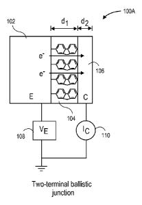
[0012] Figure 1 illustrates a schematic diagram representing (A) a two-
terminal ballistic junction and (B) a three- terminal ballistic junction, in
accordance
with an embodiment of the present invention.
[0013] Figure 2 illustrates a practical manifestation of a two-terminal
ballistic
junction containing a monolayer of fluorene as the molecular layer, in
accordance with
an embodiment of the present invention.
[0014] Figure 3 is a schematic (side view) of a two-terminal junction
modified
to include a layer of luminescent material (L) deposited on the surface of the
collector
(C), in accordance with an embodiment of the present invention.
[0015] Figure 4 illustrates (A) a side-view schematic of a three-
terminal
ballistic junction of the type
conductorl/moleculel/conductor2/molecule2/conductor3,
containing azobenzene and polythiophene layers, while (B) is a photomicrograph
of a
top view of the junction of A, showing contacts to Emitter (PPF), Base (Cu)
and
Collector (Au), in accordance with an embodiment of the present invention.
[0016] Figure 5 illustrates (A) a circuit schematic for a three-channel
monitoring of a three-terminal ballistic junction, for the case where Cu and
Au are
both biased at V=0 volts, while (B-E) are plots showing current and voltage
characteristics of the terminals during operation, in accordance with an
embodiment
of the present invention.
[0017] Figure 6 illustrates (A) a schematic of a three-terminal
ballistic
junction with resonant tunneling in the second molecular layer and (B) a plot
of
3
CA 02811223 2013-03-12
WO 2012/037474 PCT/US2011/051958
hypothetical current-voltage response of such a ballistic junction, in
accordance with
an embodiment of the present invention.
[0018] Figure 7 illustrates (A) a schematic of the general structure of
the
device 100B of Figure 1, (B) is a plot of the corresponding energy levels A,
(C) is a
diagram of a lowest unoccupied molecular orbital (LUMO) of a second molecule
resonant with the tunneling electron, (D) is a diagram showing the case of a
second
layer composed of a semiconductor (CB= conduction band, VB= valence band), and
(E) is a diagram of a semimetal with a finite density of states in the
relevant energy
range, in accordance with an embodiment of the present invention.
DETAILED DESCRIPTION
[0019] Two- and three-terminal molecular electronic devices with
ballistic
carrier transport generated via quantum mechanical tunneling or energy level
matching are described herein. The ballistic, or scattering-free regime, is
distinct from
ohmic conduction in that device operations can be performed prior to charge
carrier
scattering. Ballistic carriers have a characteristic "mean free path" which
indicates the
distance the carrier can travel through a device without scattering at
interfaces or
within materials comprising the device. In the following description, numerous
specific details are set forth, such as specific molecular layer compositions
and device
arrangements, in order to provide a thorough understanding of embodiments of
the
present invention. It will be apparent to one skilled in the art that
embodiments of the
present invention may be practiced without these specific details. In other
instances,
well-known processing or fabrication techniques, such as metal or dielectric
layer
patterning techniques, are not described in detail in order to not
unnecessarily obscure
embodiments of the present invention. Furthermore, it is to be understood that
the
various embodiments shown in the Figures are illustrative representations and
are not
necessarily drawn to scale.
[0020] Disclosed herein are two- and three-terminal molecular
electronic
devices. In one embodiment, a two-terminal molecular electronic device is
provided.
The device includes a conductorl layer/molecule I layer/conductor2 layer
junction,
wherein the total thickness of the moleculel layer and the conductor2 layers
is less
than or approximately equal to the mean free path of a charge carrier
travelling
through the layers, and wherein ballistic transport can occur for some
fraction of a
4
CA 02811223 2013-03-12
WO 2012/037474 PCT/US2011/051958
plurality of charge carriers in the layers. Ballistic carriers traverse
through moleculel
and conductor2 without scattering in the layers themselves or at their
interface.
[0021] In another embodiment, a three-terminal molecular electronic
device is
provided. The device includes a conductor] layer/moleculel layer/conductor2
layer/mo1ecu1e2 layer/conductor3 layer junction, wherein the total thickness
of the
moleculel layer, the conductor2 layer, and the mo1ecu1e2 layer is less than or
approximately equal to the mean free path of a carrier in the layers, and
wherein
ballistic transport can occur for some fraction of a plurality of carriers in
the layers.
The molecular layers represent the active transport layers. In an embodiment,
one or
more of the active transport layers is an inorganic material, that is, one or
more of the
molecular layers depicted in Figure 1 is replaced by an inorganic material. In
one
such embodiment, however, the device must include at least one molecular
layer. For
examples of such embodiments, see Figure 7, described below.
[0022] A two terminal molecular junction consists of a molecular layer
between two conductors, and shows a nonlinear response of current vs. voltage,
as has
been described in U.S. patent 7,042,006 and shown as item 260 in Figure 2
described
below. Also described therein is a three-terminal device having two molecular
layers
staggered between three conductor or contact layers. In accordance with an
embodiment of the present invention, such a two-terminal or three-terminal
device is
fabricated and operated such that carrier transport therein is "ballistic." In
one
embodiment, the term ballistic is used to mean that the electrons (or holes)
do not
scatter during transport through the molecules between conducting contacts.
Ballistic
transport is fast, operates without conventional resistance, and typically
does not
generate heat. In addition, if an upper contact and a corresponding molecular
layer are
thin compared to the mean free path of carriers, ballistic transport occurs
from a
bottom contact all the way through to the top surface of the upper contact.
[0023] Molecular devices described herein have at least one molecular
layer
covalently bonded to a conductor layer. In one such embodiment, such covalent
bonding may be irreversible. The irreversibility is thermal in the sense that
the bond
will remain intact up to temperatures of at least 300 degrees Celsius, as
distinguished
from a labile gold-thiol bond. Such an Au-S bond may be considered "covalent"
but
is also "labile," making it temperature-sensitive. The irreversible bonding
considered
for embodiments herein may be included in order to tolerate elevated operating
and
fabrication temperatures. A molecular layer may include, in an embodiment,
discrete
CA 02811223 2013-03-12
WO 2012/037474 PCT/US2011/051958
molecules, such as azobenzene and fluorene, and, in another embodiment,
conducting
polymers, such as polythiophene. For illustrative purposes, the concept of a
relationship between mean free path and ballistic transport is seen in copper.
For
example, the accepted mean free path of electrons in copper is 40 nanometers,
so
electronic conduction in bulk Cu proceeds by a series of linear trajectories
between
scattering events. (See, e.g., Ref. 15.) Thus, electrons should traverse an
average of
about 40 nanometers of copper without scattering, therefore without resistance
or heat
generation.
[0024] In an embodiment, addition of a layer of a luminescent material
onto
the surface of the upper contact of a two-terminal device permit generation of
light by
the hot electrons exiting the upper contact, or alternatively, the hot
electrons are
injected into a vacuum and collected externally. In another embodiment,
addition of a
second molecular layer onto the upper contact of a two-terminal device
followed by
addition of a third conductive contact (top contact) provides a "three-
terminal" device,
with an intermediate conducting layer (e.g., copper) disposed between two
molecular
layers.
[0025] With respect to a three-terminal device, ballistic transport may
occur
from a bottom to a top contact, through the two molecular layers and the
middle
contact. For example, in an embodiment, ballistic transport occurs if the
total
thickness of the two molecular layers and the middle contact is less than or
approximately equal to the mean free path of the electron (or hole). A three-
terminal
device may permit control of the ballistic current in various configurations
(including,
e.g., amplifier circuits), with low resistance, low heat generation, and fast
response. In
one embodiment, applications of such a three-terminal device include light
generation,
fabrication of display devices, fast yet low power amplifiers, and ultra-fast
logic
circuits.
[0026] It is noted that three-terminal devices exhibiting ballistic
transport have
been reported for inorganic semiconductor and metal oxide layers disposed
between
conducting contacts. (See, e.g., U.S. patent 7,173,275 and references therein,
U.S.
patents 4,833,517 and 5,712,491, and Heiblum, IBM J. Res. and Devel, 34, 530
(1990) and Phys. Rev. Lett. 55, 2200 (1985).) However, these devices generally
operate at low temperature and have low ballistic efficiency. By contrast, in
accordance with an embodiment of the present invention, the use of at least
one
6
CA 02811223 2013-03-12
WO 2012/037474 PCT/US2011/051958
molecular layer rather than only oxide or semiconductor layers permits the
fabrication
of much thinner layers, tunable energy levels, and possibly higher ballistic
efficiency.
[0027] In an aspect of the present invention, two-terminal and three-
terminal
molecular devices may be fabricated to have ballistic junctions. For example,
Figure
1 illustrates a schematic diagram representing (Figure 1A) a two-terminal
ballistic
junction and (Figure 1B) a three- terminal ballistic junction, in accordance
with an
embodiment of the present invention.
[0028] Referring to Figure 1, a two-terminal molecular device 100A
includes a
first conductor layer 102, a molecular layer 104, and a second conductor layer
106.
When a voltage 108 is applied across the first conductor layer 102, first
conductor
layer 102 acts as an emitter layer (E) of electrons (or holes). A current 110
can be
measured at the second conductor layer 106, which acts as a collector layer
(C).
Molecular layer 104 has a thickness d1 and second conductor layer 106 has a
thickness
d2.
[0029] In an embodiment, the two-terminal device includes an
electronically
conducting emitter layer (E), made from, for example, carbon, conducting
polymer, or
metal (or possibly a conducting metallic compound such as titanium nitride),
and a
collector layer (C) also made from a conductor. In one embodiment, the
molecular
layer 104 is deposited on the emitter layer to provide a thin film (e.g., d1
is
approximately in the range of 1-20 nanometers) composed of molecules such as,
but
not limited to, biphenyl, azobenzene, alkanes, etc. In one embodiment, the
collector
layer is also a thin layer (e.g., d2 is approximately in the range of 10-100
nanometers)
of a metal or conducting carbon in electrical contact with the molecular layer
104. In
an embodiment, two-terminal molecular device 100A may be fabricated by known
methods. (See, e.g., Refs. 1-14.) In an embodiment, notable characteristics of
the
two-terminal molecular device 100A include nonlinear resistance, weak
temperature
dependence, and strong dependence on the structure and thickness of the
molecular
layer 104. In an embodiment, second conductor layer 106 of the two-terminal
molecular electronic device 100A is composed of a semiconductor material, such
as
amorphous silicon.
[0030] In accordance with an embodiment of the present invention, the
thickness of the molecular layer 104 is less than or approximately equal to
the mean
free path of electrons in the molecular layer 104. In one embodiment, if the
thickness
of the molecular layer 104 is less than the mean free path of electrons in the
molecular
7
CA 02811223 2013-03-12
WO 2012/037474
PCT/US2011/051958
layer 104, then ballistic transport of carriers can be achieved. For example,
experimental evidence shows that for layers of a few tens of nanometers,
electrons (or
holes) do not scatter, meaning the transport is ballistic. In an embodiment,
ballistic
transport is characterized by the absence of resistance, no temperature
dependence,
minimal heat generation, and fast response time. Furthermore, in an
embodiment, if
the collector layer 106 (C in Figure 1. device 100A) is fabricated thin enough
(e.g.,
less than approximately 100 nanometers), so that the total thickness of the
molecular
layer and collector (di + d2) is short compared to the carrier mean free path,
then
electrons propagate through the molecular layer and the collector
ballistically.
[0031] Figure 2 illustrates a practical manifestation of a two-terminal
ballistic
junction 200 containing a monolayer of fluorene 210 as the molecular layer, in
accordance with an embodiment of the present invention. The emitter (E) 202 is
a
pyrolyzed photoresist film (PPF) consisting of conducting sp2 hybridized
carbon
similar to glassy carbon, and the collector (C) 204 is vapor deposited copper.
Figure
2A is a side view schematic of the junction structure 200, Figure 2B is a top
view
photomicrograph with contact probes 250 shown, and Figure 2C is an overlay of
multiple current/voltage curves for such a two-terminal ballistic junction
with an area
of approximately 0.003 square centimeters.
[0032] In accordance with an embodiment of the present invention,
carrier
transport through the two-terminal device 200 depicted in Figure 2 is
ballistic, with
the current/voltage response 260 occurring with minimal scattering. Although
structurally similar devices have been reported as -tunnel junctions" (often
based on
Al2O3 between two conductors, e.g., see Refs. 16-18), a unique feature of the
current
devices is the proximity in energy of the molecular orbitals of each molecule
in the
molecular layer 210 to the Fermi level of the contacts 202 and 204, and the
wide
variety of possible energy levels available from organic chemical structures.
Combined with the short molecular dimensions (e.g., approximately in the range
of 1-
nanometers), in one embodiment, the proximity of energies leads to high
tunneling
currents and efficient generation of energetic electrons (or holes). In
specific
embodiments, a wide range of aromatic and aliphatic molecules are available
for the
molecular layers, and they are chosen on the basis of their energy levels and
compatibility with materials and processing used to fabricate corresponding
devices.
Non-molecular materials, such as semiconductors and semi-metals, may also be
used
as the second active transport layer.
8
CA 02811223 2013-03-12
WO 2012/037474 PCT/US2011/051958
[0033] In another aspect of the present invention, if the collector
layer 106 (C
in Figure 1, device 100A) and an additional layer thereon are fabricated thin
enough
so that the total thickness of the molecular layer and collector (di + d2) as
well as the
thickness of the additional layer is shorter than or approximately equal to
the carrier
mean free path, then electrons may propagate through the molecular layer, the
collector, and the additional layer ballistically. For example, Figure 3 is a
schematic
(side view) of a two-terminal junction 300 modified to include a layer of
luminescent
material (L) 302 deposited on the suiface of the collector (C) 304, in
accordance with
an embodiment of the present invention. In an alternative embodiment (not
shown), a
luminescent material is included in the material layer of collector (C) layer,
e.g., as a
blend or mixture. In another alternative embodiment (not shown), the collector
(C) is
itself composed of a luminescent material with properties suitable to act both
as a
collector and as a source of luminescence.
[0034] In an embodiment, if ballistic electrons have sufficient energy,
they can
excite luminescence in (L) 302, to generate light. For example, referring to
Figure 3,
in one embodiment, electrons (e-) may exit the collector material 304 and
enter either
a vacuum or a layer of luminescent material 302. In a specific embodiment, if
a
vacuum, the electron may be collected by a nearby electrode, or its energy may
be
measured by a hemispherical analyzer. These "escaped" electrons may provide
information about the nature of the ballistic process or the composition of
the
collector material and its surface. In another specific embodiment, in the
case of a
luminescent material 302, the ballistic electron may create an excited state
which
emits light, with the minimum wavelength determined by the energy of the
electron.
Such light generation may be efficient and tunable with respect to color,
potentially
leading to attractive devices for area lighting and display applications, as
noted below.
In an embodiment, if a molecular layer 306 (with a thickness di), the
collector layer
304 (with a thickness d2), and the luminescent material 302 (with a thickness
d3) are
fabricated so that the total thickness of the molecular layer and the
collector layer (di
+ d2) is shorter than or approximately equal to the carrier mean free path for
those
layers, then electrons propagate through the molecular layer and the collector
layer
ballistically. It is to be understood that the carrier need not traverse the
thickness d3 of
the luminescent material ballistically.
[0035] Referring again to Figure 1, a three-terminal molecular device
100B
includes a first conductor layer 152, a first molecular layer 154, a second
conductor
9
CA 02811223 2013-03-12
WO 2012/037474
PCT/US2011/051958
layer 156, a second molecular layer 158, and a third conductor layer 160. When
a
voltage 162 is applied across the first conductor layer 152, first conductor
layer 152
acts as an emitter layer (E) of electrons (or holes). A first current 164 can
be
measured at the second conductor layer 156, which acts as a base layer (B). A
second
current 166 can be measured at the third conductor layer 160, which acts as a
collector
layer (C). First molecular layer 154 has a thickness di, second conductor
layer 156
has a thickness d7, and second molecular layer 158 has a thickness d3.
[0036] In accordance with an embodiment of the present invention, the
first
molecular layer 154 (with a thickness di), second conductor layer 156 (with a
thickness d2), and the second molecular layer 158 (with a thickness d3) are
fabricated
thin enough so that the total thickness of the first molecular layer, the
second
conductor layer, and the second molecular layer (di + d2 + d3) is short
compared to the
carrier mean free path. In that embodiment, electrons propagate through the
first
molecular layer, the second conductor layer, and the second molecular layer
ballistically. In a specific embodiment, the base thickness, d2, is similar to
the
molecular layer thicknesses, which are approximately in the range of 1-100
nanometers.
[0037] In an embodiment, the three-terminal device 100B is fabricated
by
adding a second molecular layer 158 (with a thickness d3) by spin coating or
chemical
bonding via diazonium reduction, or alternative bonding chemistry. The
junction area
may be defined by a patterned photoresist, if necessary, before adding the
molecular
layer 158. In one embodiment, the third contact (C) is applied by vapor
deposition.
Note that the designations E (emitter), B (base). and C (collector) are
familiar terms in
bipolar transistors, but it is important to understand that the device 100B
may have
very different physical principles from conventional transistors.
[0038] As an example, Figure 4A illustrates a side-view schematic of a
three-
terminal ballistic junction 400 of the type conductorl (402)/molecule1
(404)/conductor2 (406)/mo1ecu1e2 (408)/conductor3 (410), containing azobenzene
and polythiophene layers. Figure 4B is a photomicrograph 450 of a top view of
the
junction 400 of Figure 4A, showing contacts to the emitter (PPF), base (Cu)
and
collector (Au), in accordance with an embodiment of the present invention.
Thus, in
an embodiment, to fabricate a three-terminal device, a second molecular layer
and a
third conducting contact are added to a two-terminal device, in this case
consisting of
polythiophene and gold, respectively. In one embodiment, typical thicknesses
are
CA 02811223 2013-03-12
WO 2012/037474 PCT/US2011/051958
shown in Figure 4, with "e-C" being a 5 nm film of conducting carbon deposited
by
electron beam evaporation on top of the copper. Whatever the composition of
the
molecular layers and conductors, the "active" thickness (d1+d2+d3) of device
100B in
Figure 1 is less than or approximately equal to the mean free path of carriers
(electrons or holes) in those same layers. Referring again to in Figure 4B, a
photomicrograph (top view) of the finished 3-terminal device is shown, with
the
central square being the junction region (400 microns x 400 microns). Note
that, in an
embodiment, the lower three layers are identical to the three layers of a two-
terminal
device, and carrier transport should be ballistic at least in this region.
[0039] In one embodiment, a three-terminal device includes a conductorl
layer/moleculel layer/conductor2 layer/m01ecu1e2 layer/conductor3 layer
junction,
where the moleculel layer is not covalently bonded to the conductor2 layer. In
one
embodiment, one or more of the conductor layers is composed of a material such
as,
but not limited to, carbon, conducting polymers, metals, or conducting
metallic
compounds such as TiO or TiN.
[0040] In one embodiment, a three-terminal device includes a conductorl
layer/moleculel layer/conductor2 layeilmo1ecu1e2 layer/conductor3 layer
junction,
where the mo1ecu1e2 layer is not covalently bonded to the conductor2 layer or
the
conductor3 layer, or both. In one embodiment, one or more of the conductor
layers
includes a material such as, but not limited to, carbon, conducting polymers,
metals,
or conducting metallic compounds such as TiO or TiN.
[0041] In one embodiment, a three-terminal device includes a conductorl
layer/moleculel layer/conductor2 layer/m01ecu1e2 layer/conductor3 layer
junction,
where the conductor2 layer comprises a semiconductor material, such as
amorphous
silicon.
[0042] Figure 5A illustrates a circuit schematic 500 for three-channel
monitoring of a three-terminal ballistic junction, for the case where Cu and
Au are
both biased at V=0 volts, while Figure 5B is a plot of current at the emitter
terminal in
response to a voltage sweep of VppF relative to ground potential, in
accordance with an
embodiment of the present invention. Figure SC shows the collector current in
response to a voltage sweep of the Au collector with respect to ground
potential,
where the Cu and PPF are both biased at V=0 volts, indicating a resistance of
332
ohms for the base-collector junction. Figure 5D shows the collector current in
response to a voltage sweep of PPF for the case where Cu and Au are both
biased at
11
CA 02811223 2013-03-12
WO 2012/037474 PCT/US2011/051958
V=0 volts. Figure 5E shows the voltage of the base terminal as a function of
the
emitter voltage, indicating that the base is not at the desired V=0 potential,
but differs
slightly due to resistance errors in the base material. Simple calculations
with Ohm's
law shows that for the observed base voltage of 1.5 mV (when Vppr = +1 V), -
4.5 1.LA
of current are expected to flow across the collector barrier (332 ohms).
However, as
shown in Figure 5D, -5.1p,A of current are observed when VppF=+1 V, indicating
that
up to 12% of the observed collector (iAõ) current is non-classical ballistic
current, and
that 0.38% of the observed emitter current (ippF) is non-classical ballistic
current.
Retelling to circuit schematic Figure 5A, "AB" represents an azobenzene layer,
5
nanometers thick, and "PT" is a poly(3-hexylthiophene), approximately 15
nanometers thick. Referring to schematic Figure 5A, circles represent ammeters
and
rectangles are voltage sources. Polarity of the Cu and Au currents appear
opposite that
of the PPF current due to the nature of the instrument. In accordance with an
embodiment of the present invention, the extent of the ballistic nature of the
three-
terminal ballistic junction is approximately in the range of a fraction of 1%
of the
carriers to ¨15% of the carriers. In a more specific embodiment, the extent of
the
ballistic nature of the junction is in the range of approximately 5 to 15%. It
should be
understood that 15% does not represent an upper limit, and that the fraction
of carriers
traveling ballistically may be much higher, up to 100%.
[0043] The remaining carriers are presumably scattered in the Cu layer,
and
generate ic,, by conventional conduction within the Cu layer. Note that the
signs of ippF
and iA,, are opposite that of ippF simply because of the polarity of the
current
measurement. Carriers should be viewed as leaving the emitter, then either
exiting the
Cu (base), or traversing ballistically to the Au (collector). In principle, in
an
embodiment, the carriers could continue past the Au ballistically, but are
prevented
from doing so in the example shown because they are not sufficiently energetic
to
overcome the work function of Au.
[0044] In accordance with an embodiment of the present invention,
applications of a two-terminal ballistic junction include incorporation as an
electronic
circuit element. For example, in one embodiment, the two-terminal device is a
nonlinear conductor which does not exhibit conventional resistance, and
therefore
exhibits minimal heat generation. It may operate at low temperature (e.g.,
less than
approximately 5 K), and may have a high frequency response. For example, in a
specific embodiment, the transit time of a free electron across a 10 nm thick
junction
12
CA 02811223 2013-03-12
WO 2012/037474
PCT/US2011/051958
under a 1 V bias is 34 femtoseconds, corresponding to a maximum frequency of >
1013 Hz. In a particular embodiment, the actual limit is even higher due to a
low,
nonclassical effective electron mass resulting from electron delocalization. A
major
problem of existing microelectronics can be heat generation in high density
integrated
circuits. In an embodiment, this problem is circumvented if two- or three-
terminal
devices with useful electronic properties are fabricated to exhibit
essentially or only
ballistic transport. Furthermore, in one embodiment, such ballistic devices
operate
with much lower power consumption than conventional resistors and transistors.
[0045] In another embodiment, applications of a two-terminal ballistic
junction include use as a hot carrier generator. For example, in one
embodiment,
since ballistic transport through all three layers of a three-terminal device
(di+d2+d3)
is possible, as described above, two-terminal devices of the type
conductorl/moleculel/conductor2 also exhibit ballistic transport through the
second
conducting layer if d1+d2 is less than or approximately equal to the carrier
mean free
path. In a specific embodiment, such "hot electrons" may be injected into a
vacuum
(field emission) and detected with a third electrode. In another specific
embodiment,
such a device exhibits field emission at low voltage, once the applied bias
exceeds the
work function of "conductor2." Field emission may be highly sought-after for
use in
display devices based on electron impact with luminescent materials.
Furthermore, in
an embodiment, hot electrons carry information about surface and bulk
composition
of conductor2, thus providing a method for chemical characterization of the
materials
involved. For example, in a particular embodiment, adsorption of molecules to
the
conductor2 surface modulates electron emission, thus providing a method of
chemical
detection of adsorbed molecules.
[0046] In another embodiment, applications of a two-terminal ballistic
junction include use as a large area light source. For example, in one
embodiment, a
luminescent material is deposited on conductor2 and is excited by the
ballistic
electrons, emitting light. In a specific embodiment, a mixture of luminescent
materials is formulated to generate white light, possibly over a large area.
The
efficiency may be high and the manufacturing cost low, thus competing
favorably
with light emitting diodes. In a particular embodiment, large panels (e.g.,
approximately 1 square meter or larger) are fabricated to provide uniform
light output,
in various colors if desired.
13
CA 02811223 2013-03-12
WO 2012/037474 PCT/US2011/051958
[0047] In another embodiment, applications of a two-terminal ballistic
junction include use as display devices based on ballistic electrons. For
example, in
one embodiment, since the color of the emitted light is controlled in part by
the
ballistic electron energy (and therefore the applied bias, where the shortest
possible
wavelength (Xs) of the emitted light is determined by X, = h x c/(e x Vbias)
1240 eV=nm/(e x Vbias), where h is Planck's constant, c is the speed of light,
e is the
elementary charge and Vbia, is the bias voltage applied across the junction),
it is
possible to make light-emitting junctions with emission wavelengths in the
submicrometer to micrometer range. Arrays of such devices may be used to
fabricate
a display device similar to today's computer monitors. However, in a specific
embodiment, the power consumption and cost is much lower than existing devices
due to the straightforward construction.
[0048] In accordance with an embodiment of the present invention,
applications of a three-terminal ballistic junction include use as three-
terminal
electronic components. For example, as is the case with the two-terminal
ballistic
device, transport without scattering has been demonstrated for three-terminal
junctions with active thicknesses (di+d2+d3) totaling less than the mean free
path of
the carriers (electrons or holes), as described above. Minimal heat generation
and
power consumption may be two immediate consequences. In an embodiment,
however, a more fundamental consequence is the possibility that the two
molecular
layers and the intermediate conducting "base" comprise one quantum mechanical
system, with strong electronic coupling between the two molecular layers.
Thus, in
one embodiment, an electron near the conductorl/moleculel interface has a
finite
quantum-mechanical probability of appearing at the mo1ecu1e2/conductor3
interface,
hence rapid, ballistic transport occurs. Such transport may have no precedent
in
conventional microelectronics and, in a specific embodiment, is amenable to
manipulation by changes in molecular structure. Since the transit time of an
electron
across approximately 50 nanometers under 1 volt bias is < 1 picosecond, high
frequency operation above 1000 gigahertz (1 terahertz) may be possible.
[0049] In another embodiment, applications of a three-terminal
ballistic
junction include "gated" conductance in three-terminal ballistic junctions.
For
example, in one embodiment, the existence of the third terminal permits
control of
ballistic current by an applied stimulus, such as a DC or AC voltage applied
to the
"base" (conductor2). Gating is the basis of conventional tube and transistor
14
CA 02811223 2013-03-12
WO 2012/037474 PCT/US2011/051958
amplifiers, and is widely used in today's microelectronic devices. The factors
which
control gating of ballistic junctions are currently unknown but, in one
embodiment, it
is possible to control gating by the choice of molecules and conductor
(contact)
materials.
[0050] Figure 6A illustrates a schematic 600 of a three-terminal
ballistic
junction with resonant tunneling in the second molecular layer 602 and Figure
6B is a
plot 604 of hypothetical cun-ent-voltage response of such a ballistic
junction, in
accordance with an embodiment of the present invention. In one embodiment,
referring to Figures 6A and 6B, greatly enhanced transport is exhibited when
the E-B
bias produces electrons (or holes) with energies equal to a molecular orbital
in the
second molecular layer. Thus, "resonant" transport in the second molecular
layer may
be achieved. For example, in one embodiment, electrons with energies equal to
one of
the molecular orbitals in the second molecular layer have enhanced transport
across
the second layer. As YE is increased the ballistic electron energy increases,
until it
equals an orbital energy in the second layer. Since there is no bias across
the second
molecular layer, the orbital energies are not perturbed by an electric field.
In one
embodiment, such resonant transport is manifested by large increases in
current at
well defined voltages. In effect, resonant transport may be modulated by YE,
in a
fashion similar to a field effect transistor, but with a very different
underlying
mechanism. In a specific embodiment, resonant transport is very sensitive to
electron
energy, so small changes in YE yield large changes in resulting current.
[0051] Figure 7A illustrates a schematic 700 of the general structure
(where
the molecular species can be varied over a wide range of structures from those
shown)
of the device 100B of Figure 1, Figure 7B is a diagram 702 of the
corresponding
energy levels of the structure shown in Figure 7A, Figure 7C is a diagram 704
of a
lowest unoccupied molecular orbital (LUMO) of a second molecule resonant with
the
tunneling electron, Figure 7D is a diagram 706 showing the case of a second
active
transport layer composed of a semiconductor (CB= conduction band, VB= valence
band), and Figure 7E is a diagram 708 of a semimetal with a finite density of
states in
the relevant energy range, in accordance with an embodiment of the present
invention.
Thus, Figures 7B-7E illustrate energy level diagrams for a three-terminal
ballistic
junction in various manifestations. For example, referring to diagram 702,
horizontal
lines in E, B, and C are the local Fermi levels, in the case where VB = Vc.
LUMO is
the lowest unoccupied molecular orbital, which defines the energy barriers for
CA 02811223 2013-03-12
WO 2012/037474
PCT/US2011/051958
electron tunneling in the first (01) and second (02) molecular layers. As the
applied
voltage between the emitter and the base, VLB, is increased, electrons tunnel
through
the first tunneling barrier (0]), then continue ballistically through the base
and the
second molecular layer.
[00521 Referring again to Figures 7A-7E, the importance of energy
levels and
composition of the second molecular layer, with the consequence of possibly
great
versatility of the three-terminal configuration, is illustrated. Panels A and
B are the
structure and energy levels of a device with different molecules in the two
molecular
layers. For electron tunneling, the lowest unoccupied molecular orbital (LUMO)
determines the tunneling barrier, while the highest occupied molecular orbital
(HOMO) determines the barrier for hole transport. In an embodiment, tunneling
rates
are determined by the biases on all three electrodes and the thicknesses of
the
molecular layers. The case shown in plot 702 is the "non-resonant" case, where
the
molecular orbital energies are not close to the Fermi levels of the
electrodes. Diagram
704 illustrates the case of a LUMO in the second molecular layer equal to the
energy
of the hot electron leaving the base (VEB), in which significant current
enhancement is
expected. As mentioned above, one of the active transport layers may be non-
molecular. Diagram 706 depicts a semiconductor material (e.g., Si, TiO2 or
other
conductive metal oxides, etc.) as the second active transport layer, which, in
an
embodiment, enhances current once the hot electron is in the conduction band
energy
range. Diagram 708 depicts a semi-metal (e.g., bismuth) as the second active
transport layer, with a moderate but not continuous density of electronic
states (versus
a metal which is modeled as having a continuous density of electronic states).
Diagrams 704, 706, and 708 describe cases in which resonant tunneling occur.
[00531 In an embodiment, by varying the composition and energy levels
of the
molecular layers, as well as the relative biases of the three electrodes, a
variety of
electronic behaviors is possible. An additional objective of variations in
energy levels
of the first and second molecular layer may be "negative differential
resistance"
related to resonant tunneling. In a specific embodiment, it is possible to
select
molecules with suitable orbitals to produce a peak-shaped current voltage
curve.
[0054] In another embodiment, applications of a three-terminal
ballistic
junction include integration in or fabrication of logic circuits. For example,
in one
embodiment, a molecular ballistic transistor operates in a logic circuit,
similar to the
widely used transistors and diodes in computing applications. Gated operation
may
16
CA 02811223 2013-03-12
WO 2012/037474 PCT/US2011/051958
permit the three-terminal device to act as a switch, with high conductance
"ON" state
and a low conductance -OFF" state. This switching function underlies a large
fraction
of the microelectronic circuits used in today's microprocessors and digital
logic. In a
specific embodiment, using a three-terminal device with ballistic transport
has the
advantages of very little heat generation and/or very high speeds. Stated in
more
conventional terms, the 1013 second transit times predicted for a ballistic
molecular
junction correspond to switching frequencies exceeding 1000 gigahertz.
Furthermore,
in another specific embodiment, an additional attractive feature of ballistic
molecular
devices is low-voltage, low-power operation, since transport is not diffusive
and there
is no p-n "built-in" field (approximately 0.7 volts) to overcome. Low voltage,
ballistic operation may thus greatly extend battery life and conserve energy.
U.S.
patent 7,173,275 and references therein show several applications of three-
terminal
ballistic transistors fabricated without molecular layers, such as those
described in
embodiments of the present invention.
[0055] In an embodiment, applications of both a two-terminal and a
three-
terminal ballistic junction include the use of, and tailoring of, a wide range
of
molecules available for the molecular layers. For example, in one embodiment,
whether aromatic or aliphatic, whether chemically sensitive or inert, the
energy levels
and thicknesses of the molecular layers profoundly influence the electronic
properties
of the devices. Molecular structures may be designed to exhibit particular
electronic
properties, or to be made compatible with commercial processing and materials.
[0056] Thus, two- and three-terminal molecular electronic devices with
ballistic charge carrier transport have been disclosed. It is to be understood
that
higher order terminal molecular devices, e.g., 4-terminal and greater, either
on their
own or as broader devices with two- or three-terminal molecular electronic
device
portions, are considered within the spirit and scope of embodiments of the
present
invention. Devices described herein may find applications in resonant
tunneling
diodes, gated operations, high-frequency switching, logic circuits, light-
emitting
devices, chemical detection, or materials characterization.
REFERENCES
(1) McCreery, R. L.; Bergren, A. J.; Progress with Molecular Electronic
Junctions:
Meeting Experimental Challenges in Design and Fabrication; Advanced
Materials 2009, 21, 4303.
17
CA 02811223 2013-03-12
WO 2012/037474 PCT/US2011/051958
(2) Bergren, A. J.; Harris, K. D.; Deng, F.; McCreery, R.; Molecular
Electronics
using Diazonium-Derived Adlayers on Carbon with Cu Top Contacts: Critical
Analysis of Metal Oxides and Filaments; J. Phys. Condens. Matter 2008, 20,
374117.
(3) McCreery, R.; Wu, J.; Kalakodimi, R. J.; Electron Transport and Redox
Reactions in Carbon Based Molecular Electronic Junctions; Phys. Chem.
Chem. Physics. 2006, 8, 2572.
(4) Anariba, F.; Steach, J.; McCreery, R.; Strong Effects of Molecular
Structure
on Electron Transport in Carbon/molecule/Copper Electronic Junctions; J.
Phys. Chem B 2005, 109, 11163.
(5) McCreery, R.; Dieringer, J.; Solak, A. 0.; Snyder, B.; Nowak, A. M.;
McGovern. W. R.; DuVall, S.; Molecular Rectification and Conductance
Switching in Carbon-Based Molecular Junctions by Structural Rearrangement
Accompanying Electron Injection (Correction); J. Am. Chem. Soc. 2004, 126,
6200.
(6) Ranganathan, S.; Steidel, I.; Anariba, F.; McCreery, R. L.; Covalently
Bonded
Organic Monolayers on a Carbon Substrate: A New Paradigm for Molecular
Electronics; Nano Lett. 2001, /, 491.
(7) McCreery, R.; Mobley, K. J.; Wu, J.; Electronic Junction Devices
Featuring
Redox Electrodes; United States Patent # 7,737,433; 2010
(8) McCreery, R. L.; Chemical Monolayer Field Emitter Device; USA Patent #
7,019,449 B2; 2006
(9) McCreery, R.; Micro-electronic junctions and devices containing same;
United
States Patent # 7,042,006 B2; 2006
(10) McCreery, R.; Chemical Monolayer and Micro-Electronic Junctions and
Devices Containing Same; U.S. Patent # 7,112,366; 2006
(11) McCreery, R.; Electronic Junction Devices Featuring Redox Electrodes US
Patent # 7,141,299; 2006
(12) McCreery, R.; Pixel Array; US Patent # 6,919,128 B2; 2005
(13) McCreery, R.; Method for Conductance Switching in Molecular Electronic
Junctions; U.S. Patent # 6,855,950; 2005
(14) McCreery, R.; Chemical Monolayer Memory Device; U.S. Patent # 6,855,417;
2005
(15) Ashcroft, N.; Mermin, N. D.; Solid State Physics; Brooks/Cole, 1976.
18
CA 02811223 2013-03-12
WO 2012/037474
PCT/US2011/051958
(16) Mazur, U.; Hipps, K. W.; Orbital-Mediated Tunneling, Inelastic Electron
Tunneling, and Electrochemical Potentials for Metal Phthalocyanine Thin
Films; The Journal of Physical Chemistry B 1999, 103, 9721.
(17) Hipps, K. W.; Mazur, U. Inelastic electron tunneling spectroscopy. In
Handbook of Vibrational Spectroscopy; John Wiley & Sons Ltd.: Chichester,
2002; Vol. 4; pp 812.
(18) Drucker, J.; Hansma, P. K.: Emission of energetic electrons from tunnel
junctions; Phys. Rev. B 1984, 30, 4348.
(19) Ranganathan, S.; McCreery, R. L.; Electroanalytical Performance of Carbon
Films with Near-Atomic Flatness; Anal. Chem. 2001, 73, 893.
(20) Ranganathan, S.; McCreery, R. L.; Majji, S. M.; Madou, M.; Photoresist-
Derived Carbon for Microelectrochemical Applications; J. Electrochem. Soc.
2000, 147, 277
(21) McCreery, R. L.; Advanced Carbon Electrode Materials for Molecular
Electrochemistry; Chem. Rev. 2008, 108, 2646.
19