Note: Descriptions are shown in the official language in which they were submitted.
CA 02814303 2013-04-26
APPARATUS AND METHODS FOR RADIO FREQUENCY SIGNAL BOOSTERS
BACKGROUND
Field
[0001] Embodiments of the invention relate to electronic systems and,
in
particular, to radio frequency (RF) signal boosters.
Description of the Related Technology
[0002] A cellular or mobile network can include base stations for
communicating
with wireless devices located within the network's cells. For example, the
base stations can
transmit signals to wireless devices via a downlink channel and can receive
signals from the
wireless devices via an uplink channel.
[0003] A wireless device may be unable to communicate with any of the
base
stations when located in a portion of the mobile network having poor or weak
signal strength.
For example, the wireless device may be unable to communicate with a
particular base
station when the wireless device and the base station are separated by a large
distance.
Additionally, structures such as buildings or mountains can interfere with the
transmission
and/or reception of signals sent between the wireless device and a base
station.
[0004] To improve the network's signal strength and/or the network's
coverage, a
radio frequency (RF) signal booster or repeater can be used to amplify signals
in the network.
For example, the signal booster can be used to amplify or boost signals having
frequencies
associated with the frequency ranges of the network's uplink and downlink
channels. In
certain configurations, a signal booster can be used to provide network
coverage inside of a
structure, such as a home or building. However, other configurations are
possible, such as
implementations in which the signal booster is used to provide coverage to
remote network
areas or in which the signal booster is coupled to a vehicle such as an
automobile, bus, or
train and used to boost network signals as the vehicle's position changes over
time.
-1-
CA 02814303 2013-04-26
SUMMARY
100051 In one embodiment, a radio frequency signal booster includes a
first
amplification path, a second amplification path, and a third amplification
path. The first
amplification path includes a first band-pass filter configured to pass a
first channel of a first
frequency band and to attenuate a second channel of the first frequency band.
The first
channel has a first channel type and the second channel has a second channel
type.
Additionally, the first channel type comprises one of an uplink channel or a
downlink
channel, and the second channel type comprises the other of the uplink channel
and the
downlink channel. The second amplification path includes a second band-pass
filter
configured to pass a first channel of a second frequency band and to attenuate
a second
channel of the second frequency band. The first channel of the second
frequency band has
the first channel type, and the second channel of the second frequency band
has the second
channel type. The third amplification path includes a third band-pass filter
configured to pass
both the second channel of the first frequency band and the second channel of
the second
frequency band. The third band-pass filter is further configured to attenuate
both the first
channel of the first frequency band and the first channel of the second
frequency band.
100061 In another embodiment, a multiplexer includes an antenna
terminal, a first
terminal, a second terminal, a third terminal, a first band-pass filter, a
second band-pass filter,
and a third band-pass filter. The first band-pass filter is electrically
connected between the
first terminal and the antenna terminal. Additionally, the first band-pass
filter is configured
to pass a first channel of a first frequency band and to attenuate a second
channel of the first
frequency band. The first channel has a first channel type and the second
channel has a
second channel type. The first channel type comprises one of an uplink channel
or a
downlink channel, and the second channel type comprises the other of the
uplink channel and
the downlink channel. The second band-pass filter is electrically connected
between the
second terminal and the antenna terminal. The second band-pass filter is
configured to pass a
first channel of a second frequency band and to attenuate a second channel of
the second
frequency band. The first channel of the second frequency band has the first
channel type,
and the second channel of the second frequency band has the second channel
type. The third
band-pass filter is electrically connected between the third terminal and the
antenna terminal.
-2-
CA 02814303 2013-04-26
The third band-pass filter is configured to pass both the second channel of
the first frequency
band and the second channel of the second frequency band. The third band-pass
filter is
further configured to attenuate both the first channel of the first frequency
band and the first
channel of the second frequency band.
100071 In another embodiment, a method of radio frequency signal
boosting is
provided. The method includes passing a first channel of a first frequency
band using a first
band-pass filter and attenuating a second channel of the first frequency band
using the first
band-pass filter. The first channel has a first channel type and the second
channel has a
second channel type. The first channel type comprises one of an uplink channel
or a
downlink channel, and the second channel type comprises the other of the
uplink channel and
the downlink channel. The method further includes passing a first channel of a
second
frequency band using a second band-pass filter, and attenuating a second
channel of the
second frequency band using the second band-pass filter. The first channel of
the second
frequency band has the first channel type, and the second channel of the
second frequency
band has the second channel type. The method further includes passing both the
second
channel of the first frequency band and the second channel of the second
frequency band
using a third band-pass filter, and attenuating both the first channel of the
first frequency
band and the first channel of the second frequency band using the third band-
pass filter.
100081 In another embodiment, a radio frequency signal booster
includes a
housing, a first printed circuit board (PCB) positioned within a first cavity
of the housing, a
second PCB positioned within a second cavity of the housing, and a shielding
structure
positioned between the first PCB and the second PCB. The first PCB includes a
first
plurality of amplification paths configured to boost a first plurality of
radio frequency bands,
and the first plurality of radio frequency bands each have a frequency less
than about 1 GHz.
The second PCB includes a second plurality of amplification paths configured
to boost a
second plurality of radio frequency bands, and the second plurality of radio
frequency bands
each have a frequency greater than about 1 GHz.
-3-
CA 02814303 2013-04-26
- BRIEF DESCRIPTION OF THE DRAWINGS
[0009] Figure 1 is a schematic block diagram of one example
of a mobile
network.
[0010] Figure 2A is a schematic diagram of one example of a
portion of a
frequency spectrum.
[0011] Figure 2B is schematic diagram of the frequency
spectrum of Figure 2A
with annotations showing frequency locations of band-pass filter passbands
according to one
embodiment.
[0012] Figure 3 is a schematic diagram of a signal booster
for uplink and
downlink channels for two bands according to one embodiment.
[0013] Figure 4 is a schematic diagram of a signal booster
for uplink and
downlink channels for five bands according to another embodiment.
[0014] Figure 5A is a schematic diagram of a multiplexer
according to one
embodiment.
[0015] Figure 5B is a schematic diagram of a multiplexer
according to another
embodiment.
[0016] Figure 6A is a perspective view of a signal booster
in accordance with one
embodiment.
[0017] Figure 6B is a top plan view of the signal booster of
Figure 6A with a top
cover removed and with a first metal layer removed.
[0018] Figure 6C is a bottom plan view of the signal booster
of Figure 6A with a
bottom cover removed and with a portion of a second metal layer removed.
[0019] Figure 6D is a cross-section of the signal booster of
Figures 6A-6C taken
along the lines 6D-6D.
DETAILED DESCRIPTION OF EMBODIMENTS
[0020] The following detailed description of certain
embodiments presents
various descriptions of specific embodiments of the invention. However, the
invention can
be embodied in a multitude of different ways as defined and covered by the
claims. In this
-4-
CA 02814303 2013-04-26
description, reference is made to the drawings where like reference numerals
may indicate
identical or functionally similar elements.
[0021]
Figure 1 is a schematic block diagram of one example of a mobile
network 10. The mobile network 10 includes a base station 1, a signal booster
2, a plurality
of mobile devices 3a-3c (three shown), and a network device 4.
100221 The
signal booster 2 is electrically coupled to a first antenna 5a and to a
second antenna 5b. The signal booster 2 can retransmit signals to and receive
signals from
the base station 1 using the first antenna 5a, and can retransmit signals to
and receive signals
from the plurality of mobile devices 3a-3c and/or the network device 4 using
the second
antenna 5b. For example, the signal booster 2 can retransmit signals to the
base station 1
over one or more uplink channels, and can receive signals from the base
station 1 over one or
more downlink channels. Additionally, the signal booster 2 can retransmit
signals to the
plurality of mobiles devices 3a-3c and/or the network device 4 over one or
more downlink
channels, and can receive signals from the devices over one or more uplink
channels. In one
embodiment, the first antenna 5a is an outdoor antenna positioned external to
a structure such
as a home or building and the second antenna 5a is an indoor antenna
positioned within the
structure. However, other configurations are possible. In the illustrated
configuration, the
first and second antennas 5a, 5b can be external to the signal booster 2, and
can be connected,
using, for example, cables. However, other configurations are possible,
including, for
example, configurations in which the antennas are integrated as part of a
signal booster.
While illustrated with a common housing for boosting all frequency bands of
interest, the
teachings herein are applicable to configurations in which the signal booster
2 is implemented
in multiples boxes or housings that communicate with one another, such as over
a wireless
communication channel at different frequency than the frequency bands the
signal booster 2
boosts.
100231
Although Figure 1 illustrates the signal booster 2 as communicating with
one base station, the signal booster 2 typically communicates with multiple
base stations. For
example, the signal booster 2 can be used to communicate with base stations
associated with
different cells of a network. Furthermore, in certain implementations, the
signal booster 2
can communicate with base stations associated with different networks,
including, for
-5-
CA 02814303 2013-04-26
example, networks associated with different wireless carriers and/or networks
associated with
different RF frequencies or bands.
[0024] For example, the mobile devices 3a-3c and/or the network device
4 can
communicate at least in part over multiple frequency bands, including, for
example,
Universal Mobile Telecommunications System (UMTS) Band II, Band IV, Band V,
Band
XII, and/or Band XIII. For instance, in one example, the first mobile device
3a can operate
using Advanced Wireless Services (AWS) (Band IV), the second mobile device 3b
can
operate using Personal Communication Services (PCS) (Band II), and the third
mobile
device 3c can operate using Cellular (CLR) services (Band V). Furthermore, in
certain
configurations, all or a subset of the mobile devices 3a-3c and/or the network
device 4 can
communicate using Long Term Evolution (LTE), and may transmit and receive Band
XII
signals, Band XIII signals, and/or signals associated with other LTE bands.
Although
specific examples of frequency bands and communication technologies have been
described
above, the teachings herein are applicable to a wide range of frequency bands
and
communications standards.
[0025] Accordingly, the signal booster 2 can be configured to boost
signals
associated with multiple frequency bands so as to improve network reception
for each of the
mobile devices 3a-3c and the network device 4. Configuring the signal booster
2 to service
multiple frequency bands can improve network signal strength for multiple
devices. For
example, the signal booster 2 can improve network signal strength of devices
using the same
or different frequency bands, the same or different wireless carriers, and/or
the same or
different wireless technologies. Configuring the signal booster 2 as a multi-
band repeater can
avoid the cost of separate signal boosters for each specific frequency band
and/or wireless
carrier. Additionally, configuring the signal booster 2 as a multi-band
repeater can also ease
installation, reduce cabling, and/or issues associated with combining multiple
repeaters.
[0026] The plurality of mobile devices 3a-3c can represent a wide
range of mobile
or portable communication devices, including, for example, multi-band mobile
phones. The
network device 4 can represent a wide range of other devices configured to
communicate
over one or more mobile networks, including, for example, computers,
televisions, modems,
routers, or other electronics. In one embodiment, the network device 4 is
another signal
-6-
CA 02814303 2013-04-26
booster. Although Figure 1 illustrates the signal booster 2 as communicating
with three
mobile devices 3a-3c and one network device 4, the signal booster 2 can be
used to
communicate with more or fewer mobile devices and/or more or fewer network
devices.
[0027] Figure 2A is a schematic diagram of one example of a portion of
a
frequency spectrum 20. The frequency spectrum 20 includes a Band XII uplink
channel, a
Band XII downlink channel, a Band XIII downlink channel, a Band XIII uplink
channel, a
Band V uplink channel, a Band V downlink channel, a Band IV uplink channel, a
Band II
uplink channel, a Band II downlink channel, and a Band IV downlink channel.
The
frequency spectrum 20 of Figure 2A illustrates one example of the frequency
bands that a
signal booster described herein can be used to boost. However, other
configurations are
possible, such as implementations in which the signal booster amplifies more
or fewer
frequency bands and/or a different combination of frequency bands.
[0028] In certain implementations, the Band XII uplink channel can
have a
frequency range of about 698 MHz to about 716 MHz, and the Band XII downlink
channel
can have a frequency range of about 728 MHz to about 746 MHz. Additionally, in
certain
implementations the Band XIII uplink channel can have a frequency range of
about 776 MHz
to about 787 MHz, and the Band XIII downlink channel can have a frequency
range of about
746 MHz to about 757 MHz. Furthermore, in certain implementations the Band V
uplink
channel can have a frequency range of about 824 MHz to about 849 MHz, and the
Band V
downlink channel can have a frequency range of about 869 MHz to about 894 MHz.
Additionally, in certain implementations the Band IV uplink channel can have a
frequency
range of about 1710 MHz to about 1755 MHz, and the Band IV downlink channel
can have a
frequency range of about 2110 MHz to about 2155 MHz. Furthermore, in certain
implementations the Band II uplink channel can have a frequency range of about
1850 MHz
to about 1910 MHz, and the Band II downlink channel can have a frequency range
of about
1930 MHz to about 1990 MHz.
[0029] Although specific frequency ranges have been provided above,
persons of
ordinary skill in the art will appreciate that the frequencies of the bands
can vary by
geographical region and/or can change over time based on regulations set by
governing
-7-
CA 02814303 2013-04-26
agencies such as the Federal Communications Commission (FCC) or the Canadian
Radio-
television and Telecommunications Commission (CRTC).
[0030] Certain signal boosters can use a separate amplification path
for each
channel of each frequency band that the signal booster is used to boost or
repeat. For
example, each amplification path of the signal booster can include a band-pass
filter having a
passband for passing a particular uplink or downlink channel while attenuating
or blocking
other frequencies. Configuring the signal booster in this manner can aid in
maintaining the
booster's compliance with communication standards and/or regulator rules, such
as those
limiting spurious and/or out-of-band emissions.
[0031] The radio frequency spectrum has become increasingly crowded
with
signals as mobile technologies have advanced and the demand for high speed
wireless
communication has expanded. For example, there has been an increase in a
number and
proximity of frequency bands that are being utilized by mobile devices and
networks.
[0032] The increased crowding of the radio frequency spectrum has
constrained
the design and development of signal boosters, particular multi-band signal
boosters that
provide boosting across multiple frequency bands, including, for example,
adjacent frequency
bands. For example, a band-pass filter used to select a particular uplink or
downlink channel
for boosting can have a non-ideal passband associated with roll-off near the
passband's
edges. The filter's roll-off can lead to an increase in undesired spurious
and/or out-of-band
emissions associated with amplification of signals outside of the particular
channel's
frequency band. Although a particular uplink or downlink channel may be
selected by using
a relatively sharp filter such as a cavity filter, such filters can be
prohibitive in cost and/or
size.
[0033] Provided herein are apparatus and methods for RF signal
boosters. In
certain implementations, a multi-band signal booster is provided for boosting
the uplink and
downlink channels of at least a first frequency band and a second frequency
band. The first
and second frequency bands can be closely positioned in frequency, and the
first and second
frequency bands can include uplink or downlink channels that are adjacent. For
example, the
duplex of the first and second frequency bands can be reversed such that the
order in
frequency of the first frequency band's uplink and downlink channels is
flipped or reversed
-8-
CA 02814303 2013-04-26
relative to the second frequency band's uplink and downlink channels. However,
other
configurations are possible, such as when two frequency bands have that are
disjoint, and the
uplink and/or downlink channels of the bands are adjacent.
[0034] In certain configurations, the downlink channels of the first
and second
channels are adjacent, and the signal booster includes a first amplification
path for boosting
the uplink channel of the first frequency band, a second amplification path
for boosting the
uplink channel of the second frequency band, and a third amplification path
for boosting the
downlink channels of the first and second frequency bands. For example, the
first
amplification path can include a first band-pass filter for passing the first
frequency band's
uplink channel and for attenuating other frequencies such as the first
frequency band's
downlink channel, and the second amplification path can include a second band-
pass filter for
passing the second frequency band's uplink channel and for attenuating other
frequencies
such as the second frequency band's downlink channel. Additionally, the third
amplification
path can include a third band-pass filter for passing the downlink channels of
the first and
second frequency bands and for attenuating other frequencies such as the
uplink channels of
the first and second frequency bands. Thus, the signal booster can include a
shared
amplification path that operates to boost or repeat the downlink channels of
adjacent
frequency bands.
[0035] However, in other configurations, the uplink channels of the
first and
second channels are adjacent, and the signal booster includes a first
amplification path for
boosting the downlink channel of the first frequency band, a second
amplification path for
boosting the downlink channel of the second frequency band, and a third
amplification path
for boosting the uplink channels of the first and second frequency bands.
[0036] The signal boosters described herein can be used to boost
multiple
frequency bands, thereby improving signal strength for devices using different
communications technologies and/or wireless carriers. Configuring the signal
booster in this
manner can avoid the cost of multiple signal boosters, such as having a
specific signal
booster for each frequency band. Additionally, the signal boosters can have
reduced
component count and/or size, since band-pass filters, amplifiers, attenuators
and/or other
circuitry can be shared for at least two channels. Furthermore, the signal
boosters herein can
-9-
CA 02814303 2013-04-26
be implemented without the cost of filters with relatively sharp passbands,
such as cavity
filters, which can have a high cost and/or a large area. Thus, the signal
boosters herein can be
implemented using filters having a relatively low cost and/or a relatively
small size, such as
surface acoustic wave (SAW) filters and/or ceramic filters.
[0037] Figure 2B is schematic diagram of the frequency spectrum of
Figure 2A
with annotations showing frequency locations of band-pass filter passbands
according to one
embodiment.
[0038] In the illustrated configuration, a first band-pass filter
passband 31 has
been implemented to pass or select a Band XII uplink channel, and a second
band-pass filter
passband 32 has been implemented to pass a Band XIII uplink channel.
Furthermore, a third
band-pass filter passband 33 has been implemented to pass both a Band XII
downlink
channel and a Band XIII downlink channel. Additionally, a fourth band-pass
filter
passband 34 has been implemented to pass a Band V uplink channel, and a fifth
band-pass
filter passband 35 has been implemented to pass a Band V downlink channel.
Furthermore, a
sixth band-pass filter passband 36 has been implemented to pass a Band IV
uplink channel,
and a seventh band-pass filter passband 37 has been implemented to pass a Band
II uplink
channel. Additionally, an eighth band-pass filter passband 38 has been
implemented to pass
a Band II downlink channel, and a ninth band-pass filter passband 39 has been
implemented
to pass a Band IV downlink channel. Although Figure 2B illustrates a single
passband for
each frequency channel, a signal booster can include a plurality of band-pass
filters that are
cascaded, with or without intervening circuitry, to achieve an overall channel
filtering.
[0039] As used herein, a band-pass filter can "pass" a particular
frequency
channel when the frequency channel is substantially within the band-pass
filter's passband,
even when the passband provides gain or loss in the passband. Accordingly, the
teachings
herein are not limited to band-pass filters having unity-gain passbands.
[0040] As shown in Figure 2B, the third band-pass filter passband 33
advantageously passes the downlink channels of both Band XII and Band XIII,
which are
adjacent frequency bands. The illustrated configuration takes advantage of the
reverse duplex
of the Band XIII frequency band relative to that of the Band XII frequency
band. For
example, a typical frequency band such as Band XIII, Band II, Band IV, and
Band V uses an
-10-
CA 02814303 2013-04-26
uplink channel that is at a lower frequency than a corresponding downlink
channel of the
same band. However, Band XIII uses a reverse configuration in which the
downlink channel
is at a lower frequency relative to the uplink channel. Configuring a signal
booster to have a
band-pass filter that passes both the Band XII and Band XIII downlink signals
can avoid a
need for sharp band-pass filters for separately filtering the downlink bands,
which can be
difficult using relative small and/or low-cost filters such as SAW filters
and/or ceramic
filters, which can have a non-ideal passband and can provide insufficient
channel filtering or
selectivity.
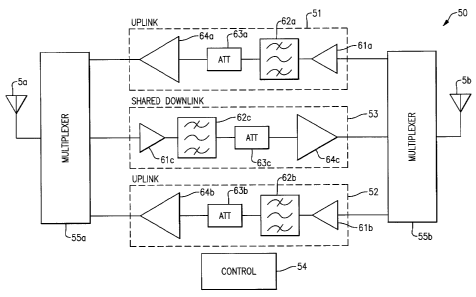
[0041] Figure 3 is a schematic diagram of a signal booster 50 for
uplink and
downlink channels for two bands according to one embodiment. The signal
booster 50
includes first and second multiplexers 55a, 55b, first to third amplification
paths or circuits
51-53, and a control circuit 54. In the illustrated configuration, the signal
booster 50 is
electrically coupled to the first and second antennas 5a, 5b, such as by
cables or wires.
However, other configurations are possible, including, for example,
configurations in which
the antennas are integrated with a signal booster.
[0042] The first multiplexer 55a includes a first terminal
electrically connected to
an output of the first amplification path 51, a second terminal electrically
connected to an
output of the second amplification path 52, a third terminal electrically
connected to an input
of the third amplification path 53, and an antenna terminal electrically
connected to the first
antenna 5a. The second multiplexer 55b includes a first terminal electrically
connected to an
input of the first amplification path 51, a second terminal electrically
connected to an input of
the second amplification path 52, a third terminal electrically connected to
an output of the
third amplification path 53, and an antenna terminal electrically connected to
the second
antenna 5b.
[0043] The first amplification path 51 includes a first low noise
amplifier
(LNA) 61a, a first band-pass filter 62a, a first attenuator 63a, and a first
power amplifier
(PA) 64a. The first LNA 61a, the first band-pass filter 62a, the first
attenuator 63a, and the
first PA 64a are cascaded with an input of the first LNA 61a operating as the
first
amplification path's input and with an output of the first PA 64a operating as
the first
amplification path's output. The second amplification path 52 includes a
second LNA 61b, a
-11-
CA 02814303 2013-04-26
second band-pass filter 62b, a second attenuator 63b, and a second PA 64b. The
second
LNA 61b, the second band-pass filter 62b, the second attenuator 63b, and the
second PA 64b
are cascaded with an input of the second LNA 61b operating as the second
amplification
path's input and with an output of the second PA 64b operating as the second
amplification
path's output. The third amplification path 53 includes a third LNA 61c, a
third band-pass
filter 62c, a third attenuator 63c, and a third PA 64c. The third LNA 61c, the
third band-pass
filter 62c, the third attenuator 63c, and the third PA 64c are cascaded with
an input of the
third LNA 61c operating as the third amplification path's input and with an
output of the
third PA 64c operating as the third amplification path's output.
[0044] In one embodiment, the gain of each of the first to third
amplification
paths 51-53 is selected to be in the range of about 10 dB to about 90 dB. In
certain
configurations, the gain of one or more of the first to third amplification
paths 51-53 can be
externally controlled, such as by using one or more switches and/or by using
digital
configuration. Although one example of gain values has been provided, other
configurations
are possible.
[0045] The first to third LNAs 61a-61c can provide low noise
amplification for
the first to third amplification paths 51-53, respectively. In certain
implementations, the first
to third LNAs 61a-61c can be used to amplify signals having a relatively small
amplitude
while adding or introducing a relatively small amount of noise. For example,
in one
embodiment, each of the LNAs 61a-61c has a noise figure of 1 dB or less.
However, other
configurations are possible.
[0046] The first to third band-pass filters 62a-62c include inputs
electrically
coupled to outputs of the first to third LNAs 61a-61c, respectively. The first
to third
band-pass filters 62a-62c can filter the frequency content of the amplified
signals generated
by the first to third LNAs 61a-61c, respectively. Additional details of the
first to third
band-pass filters 62a-62c will be described further below.
[0047] The first to third attenuators 63a-63c can be used to attenuate
the filtered
signals generated by the first to third band-pass filters 62a-62c,
respectively. The first to third
attenuators 63a-63c can be used to limit a gain of the first to third
amplification paths 51-53,
respectively. For example, it can be desirable to provide attenuation in one
or more of the
-12-
CA 02814303 2013-04-26
first to third amplification paths 51-53, such as in configurations in which
one or more of the
input signals to the amplification paths has a relatively large amplitude,
which can occur
when the signal booster 50 is positioned relatively close to a base station.
In one
embodiment, the attenuation of the first to third attenuators 63a-63c can be
controlled using
one or more processing or control units. For example, one or more embedded
CPUs can be
used to provide gain control, such as programmable gain control. In certain
implementations,
the first to third attenuators 63a-63c can be implemented using analog
attenuation
components. However, other configurations are possible, such as
implementations using
digital attenuators, such as digital step attenuators.
100481 The first to third PAs 64a-64c can be used to amplify the
attenuated
signals generated by the first to third attenuators 63a-63c, respectively. The
first to third PAs
64a-64c can be used to generate amplified RF output signals that have a
magnitude suitable
for transmission via an antenna. The first to third PAs 64a-64c can be
implemented using
single or multi-stage configurations, including, for example, multi-stage
configurations using
automatic gain control (AGC).
100491 The control circuit 54 can be used to control the operation of
the circuitry
of the signal booster 50. For example, in certain implementations, the control
circuit 54 can
be used to control the level of attenuation of the first to third attenuators
63a-63c, an amount
of gain of the first to third PAs 64a-64c and/or the first to third LNAs 61a-
61c, and/or to
provide other control operations in signal booster 50. For clarity of the
figures, connections
and control signals generated by the control circuit 54 have been omitted.
Additionally,
although not illustrated in Figure 3, the signal booster 50 can include
additional circuitry such
as directional couplers, which can aid the control circuit 54 in controlling
output power levels
of the first to third amplification paths 51-53. Accordingly, in certain
implementations the
control circuit 54 can operate to provide automatic gain control (AGC). The
control
circuit 54 can also operate to provide other functionality, including, for
example, automatic
oscillation detection and/or automatic shutdown to prevent interference with
base stations.
100501 The first and second multiplexers 55a, 55b can be used to
provide
multiplexing between the first to third amplification paths 51-53 and the
first and second
antennas 5a, 5b, respectively. For example, the first multiplexer 55a can be
used to combine
-13-
CA 02814303 2013-04-26
the amplified output signals from the first and second amplification paths 51,
52 for
transmission via the first antenna 5a, and to filter a receive signal received
on the first
antenna 5a to provide an input signal to the third amplification path 63.
Additionally, the
second multiplexer 55b can be used to provide the amplified output signal from
the third
amplification path 55b to the second antenna 5b, and to filter a receive
signal received on the
second antenna 5b to provide appropriate input signals to the first and second
amplification
paths 51, 52.
[0051] In certain implementations, the first multiplexer 55a can
include a
band-pass filter associated with each of the multiplexer's first to third
terminals.
Additionally, the second multiplexer 55b can include a band-pass filter
associated with each
of the multiplexer's first to third terminals. The band-pass filter associated
with a particular
terminal can be configured to pass frequencies corresponding to those of an
associated
amplification path that is connected to the terminal. For example, in certain
configurations,
the band-pass filters of the multiplexers 55a, 55b have a passband similar to
that of a
corresponding one of the band-pass filters 62a-62c of the amplification paths
51-53. One
example of a suitable implementation of the first and second multiplexers 55a,
55b can be
similar to that described below with respect to Figure 5A.
[0052] Furthermore, in certain implementations, one or both of the
first and
second multiplexers 55a, 55b can be omitted. For example, in one embodiment,
the signal
booster 50 omits the first and second multiplexers 55a, 55b in favor of using
a separate
antenna at the input and output of each of the amplification paths 51-53.
100531 The signal booster 50 can be used to boost the uplink and
downlink
channels of first and second frequency bands that are adjacent or closely
positioned in
frequency, such as when adjacent frequency bands have a duplex that is
reversed. For
example, in one embodiment, the signal booster 50 is used to boost Band XII
and Band XIII,
which are adjacent in frequency and have uplink and downlink channels that are
flipped or
reversed in frequency such that the Band XII downlink channel and the Band
XIII downlink
channel are positioned between the Band XII uplink channel and the Band XIII
uplink
channel. For example, the Band XII downlink channel can have a greater
frequency than the
-14-
CA 02814303 2013-04-26
Band XII uplink channel, and the Band XIII uplink channel can have a greater
frequency than
the Band XIII downlink channel.
[0054] Additionally, the signal booster 50 includes the first and
second
amplification paths 51, 52, which can be used to amplify the uplink channels
of the first and
second bands. Furthermore, the signal booster 50 includes the third
amplification path 53,
which operates as a shared amplification path that boosts both the downlink
channel of the
first frequency band and the downlink channel of the second frequency band.
Thus, in
contrast to a conventional signal booster that includes a separate
amplification path for each
frequency channel that is boosted, the illustrated configuration includes a
shared
amplification path for amplifying adjacent downlink channels.
[0055] To provide suitable channel filtering, the first band-pass
filter 62a can pass
the first frequency band's uplink channel and attenuate the first frequency
band's downlink
channel. Additionally, second band-pass filter 62b can pass the second
frequency band's
uplink channel and attenuate the second frequency band's downlink channel.
Furthermore,
the third band-pass filter 62c can pass the downlink channels of both the
first and second
frequency bands and attenuate the uplink channels of both the first and second
frequency
bands. Thus, the third amplification path 53 is shared between the downlink
channels of the
first and second frequency bands and operates to simultaneously boost or
repeat the downlink
channels. Since the third amplification path 53 boosts the downlink channels
of both the first
and second frequency bands, relatively sharp filters need not be used to
separately filter these
channels. Thus, the first to third band-pass filters 62a-62c can be
implemented using filters
having a relatively low cost and/or a relatively small size, such as surface
acoustic wave
(SAW) and/or ceramic filters.
[0056] Although the signal booster 50 has been described in the
context of a
single amplification path boosting multiple downlink channels, the teachings
herein are
applicable to configurations in which a single amplification path is used to
boost multiple
uplink channels. For example, the teachings herein are applicable to
configurations in which
a shared amplification path is used to boost the uplink channels of two
frequency bands that
are adjacent, such as when the duplex of the first and second frequency bands
is reversed
such that the bands' uplink channels are positioned between the bands'
downlink channels.
-15-
CA 02814303 2013-04-26
[0057] In one embodiment, the adjacent uplink channels or the adjacent
downlink
channels of the first and second frequency bands are separated in frequency by
less than about
MHz. Furthermore, in certain implementations, the adjacent uplink channels or
the
adjacent downlink channels of the first and second frequency bands are
abutting, such that
there is substantially no separation or gap (e.g., about 0 MHz) between the
channel
frequencies.
[0058] Although one implementation of a signal booster is illustrated
in Figure 3,
other configurations are possible. For example, the signal booster can include
more or fewer
amplifications paths. Additionally, one or more of the amplification paths can
be modified to
include more or fewer components and/or a different arrangement of components.
For
example, in certain implementations, the order of a band-pass filter and an
attenuator can be
reversed in a cascade, the band-pass filters can be positioned before the LNAs
in one or more
of the cascades, and/or additional components can be inserted in the cascade.
[0059] Figure 4 is a schematic diagram of a signal booster 100 for
uplink and
downlink channels for five bands according to another embodiment. The signal
booster 100
includes the control circuit 54, first to fourth multiplexers 112a-112d, first
and second
diplexers 111a, 111b, and first to ninth amplification paths or circuits 101-
109. The signal
booster 100 is electrically coupled to the first and second antennas 5a, 5b.
[0060] The first diplexer 111a includes an antenna terminal
electrically connected
to the first antenna 5a, a first terminal electrically connected to an antenna
terminal of the
first multiplexer 112a, and a second terminal electrically connected to an
antenna terminal of
the third multiplexer 112c. The second diplexer 111b includes an antenna
terminal
electrically connected to the second antenna 5b, a first terminal electrically
connected to an
antenna terminal of the second multiplexer 112b, and a second terminal
electrically
connected to an antenna terminal of the fourth multiplexer 112d.
[0061] The first multiplexer 112a further includes a first terminal
electrically
connected to an output of the first amplification path 101, a second terminal
electrically
connected to an output of the second amplification path 102, a third terminal
electrically
connected to an input of the third amplification path 103, a fourth terminal
electrically
connected to an output of the fourth amplification path 104, and a fifth
terminal electrically
-16-
CA 02814303 2013-04-26
connected to an input of the fifth amplification path 105. The second
multiplexer 112b
further includes a first terminal electrically connected to an input of the
first amplification
path 101, a second terminal electrically connected to an input of the second
amplification
path 102, a third terminal electrically connected to an output of the third
amplification
path 103, a fourth terminal electrically connected to an input of the fourth
amplification
path 104, and a fifth terminal electrically connected to an output of the
fifth amplification
path 105.
[0062] The third multiplexer 112c includes a first terminal
electrically connected
to an input of the sixth amplification path 106, a second terminal
electrically connected to an
output of the seventh amplification path 107, a third terminal electrically
connected to an
input of the eighth amplification path 108, and a fourth terminal electrically
connected to an
output of the ninth amplification path 109. The fourth multiplexer 112d
includes a first
terminal electrically connected to an output of the sixth amplification path
106, a second
terminal electrically connected to an input of the seventh amplification path
107, a third
terminal electrically connected to an output of the eighth amplification path
108, and a fourth
terminal electrically connected to an input of the ninth amplification path
109.
[0063] In the illustrated configuration, the first amplification path
101 can provide
boosting to a Band XII uplink channel, and the second amplification path 102
can provide
boosting to a Band XIII uplink channel. Furthermore, the third amplification
path 103 can
provide boosting to both the Band XII and Band XIII downlink channels.
Additionally, the
fourth amplification path 104 can provide boosting to the Band V uplink
channel, and the
fifth amplification path 105 can provide boosting to the Band V downlink
channel.
Furthermore, the sixth amplification path 106 can provide boosting to the Band
IV downlink
channel, and the seventh amplification path 107 can provide boosting to the
Band IV uplink
channel. Additionally, the eighth amplification path 108 can provide boosting
to the Band II
downlink channel, and the ninth amplification path 109 can provide boosting to
the Band II
uplink channel.
[0064] The first and second multiplexers 112a, 112b can provide
multiplexing
operations for the first to fifth amplification paths 101-105. The first and
second
multiplexers 112a, 112b can include a band-pass filter for each of the
multiplexers' first to
-17-
CA 02814303 2013-04-26
fifth terminals. The band-pass filters can have passbands positioned at
frequencies
corresponding to the uplink or downlink channels of an associated
amplification path.
Additionally, the third and fourth multiplexers 112c, 112d can provide
multiplexing
operations for the sixth to ninth amplification paths 106-109. The third and
fourth
multiplexers 112c, 112d can include a band-pass filter for each of the
multiplexers' first to
fourth terminals. The band-pass filters can have passbands positioned at
frequencies
corresponding to the uplink or downlink channels of an associated
amplification path.
100651 The first diplexer 111a can be used to multiplex signals on the
antenna
terminals of the first and third multiplexers 112a, 112c, and can provide the
multiplexed
signal to the first antenna 5a. Additionally, the second diplexer 111b can be
used to
multiplex signals on the antenna terminals of the second and fourth
multiplexers 112b, 112d,
and can provide the multiplexed signal to the second antenna 5b. Including the
first and
second diplexers 111a, 111b in the signal booster 100 can aid the signal
booster 100 in
operating over disjoint frequency bands by multiplexing signals separated by a
relatively
large frequency difference. For example, in the illustrated configuration, the
first and second
diplexers 111a, 111b have been used to multiplex Band XII, Band XIII, and Band
V signals
with Band II and Band IV signals.
[0066] The first to ninth amplification paths 101-109 include
different
combinations of components, such as amplifiers, attenuators, and band-pass
filters, selected
to achieve an overall amplification characteristic desirable for a particular
band.
100671 In the illustrated configuration, the first amplification path
101 includes a
cascade of an LNA 121a, a first band-pass filter 122a, a power level control
block or
circuit 123a, a first intermediate amplifier or gain block 124a, a second band-
pass filter 125a,
an attenuator 126a, a second gain block 127a, a third band-pass filter 128a, a
third gain block
129a, a fourth band-pass filter 130a, and a power amplifier 132a.
Additionally, the second
amplification path 102 includes a cascade of an LNA 121b, a first band-pass
filter 122b, a
power level control block 123b, a first gain block 124b, an attenuator 126b, a
second
band-pass filter 125b, a second gain block 127b, a third band-pass filter
128b, a third gain
block 129b, a fourth band-pass filter 130b, and a power amplifier 132b.
Furthermore, the
third amplification path 103 includes a cascade of an LNA 121c, a power level
control block
-18-
CA 02814303 2013-04-26
_
123c, a first band-pass filter 122c, a first gain block 124c, an attenuator
126c, a second gain
block 127c, a second band-pass filter 125c, a third gain block 129c, a fourth
gain block 131c,
a third band-pass filter 128c, and a power amplifier 132c. Additionally, the
fourth
amplification path 104 includes a cascade of an LNA 121d, a first band-pass
filter 122d, a
power level control block 123d, a first gain block 124d, a second band-pass
filter 125d, an
attenuator 126d, a second gain block 127d, a third band-pass filter 128d, a
third gain
block 129d, and a power amplifier 132d. Furthermore, the fifth amplification
path 105
includes a cascade of an LNA 121e, a first band-pass filter 122e, a power
level control
block 123e, a first gain block 124e, a second band-pass filter 125e, an
attenuator 126e, a
second gain block 127e, a third band-pass filter 128e, a third gain block
129e, and a power
amplifier 132e.
[0068] Additionally, in the illustrated configuration, the
sixth amplification
path 106 includes a cascade of an LNA 121f, a first band-pass filter 122f, a
power level
control block 123f, a first gain block 124f, a second band-pass filter 125f,
an attenuator 126f,
a third band-pass filter 128f, a second gain block 127f, a fourth band-pass
filter 130f, a third
gain block 129d, and a power amplifier 132f. Furthermore, the seventh
amplification
path 107 includes a cascade of an LNA 121g, a first band-pass filter 122g, a
power level
control block 123g, a first gain block 124g, a second band-pass filter 125g,
an
attenuator 126g, a second gain block 127g, a third band-pass filter 128g, a
third gain block
129g, a fourth band-pass filter 130g, a fourth gain block 131g, and a power
amplifier 132g.
Additionally, the eighth amplification path 108 includes a cascade of an LNA
121h, a first
band-pass filter 122h, a power level control block 123h, a first gain block
124h, a second
band-pass filter 125h, an attenuator 126h, a third band-pass filter 128h, a
second gain block
127h, a fourth band-pass filter 130h, a third gain block 129h, and a power
amplifier 132h.
Furthermore, the ninth amplification path 109 includes a cascade of an LNA
121i, a first
band-pass filter 122i, a power level control block 123i, a first gain block
124i, an
attenuator 126i, a second band-pass filter 125i, a second gain block 127i, a
third band-pass
filter 128i, a third gain block 129i, and a power amplifier 132i.
[0069] The signal booster 100 of Figure 4 is similar to the
signal booster 50 of
Figure 3, except that the signal booster 100 of Figure 4 has been expanded to
provide
-19-
CA 02814303 2013-04-26
boosting to five frequency bands and has been adapted to include additional
filters, amplifiers
and other circuitry, such as additional components in cascades associated with
the
amplification paths. In the illustrated configuration, each of the
amplification paths 101-109
includes an LNA, a power amplifier, an attenuator, and at least one band-pass
filter.
[0070] As shown in Figure 4, a type, number, and/or order of the
components in
an amplification path can be selected to provide a desired amplification
characteristic for a
particular frequency channel. For example, a number of gain blocks can be
selected to
achieve a desired amplification characteristic depending upon the band and
channel(s) being
amplified, while a number of pass-band filters can be selected to achieve a
desired filtering
characteristic for the channel(s).
[0071] In certain configurations, the power level control blocks 123a-
123i are
included to adjust the gain of the first to ninth amplification paths 101-109,
respectively. For
example, in certain implementations, the power level control blocks 123a-123i
can be used to
adjust or limit the gain when the gain of an associated amplification path
exceeds a maximum
power threshold level. However, in other configurations, one or more of the
power level
control blocks 123a-123i can be omitted.
[0072] In the illustrated configuration, the signal booster 100
includes the third
amplification path 103, which has been configured to boost both a Band XII
downlink
channel and a Band XIII downlink channel. The third amplification path 103
includes first to
third band-pass filters 122c, 125c, 128c, each of which can have a passband
configured to
pass both the Band XII and Band XIII downlink channels while attenuating other
frequency
components. Thus, in contrast to the signal booster 50 of Figure 3 which
includes one
band-bass filter 62b in the third amplification path 53, the signal booster
100 illustrates a
configuration using three band-pass filters 122c, 125c, 128c in the third
amplification
path 103. Using a plurality of band-pass filters in an amplification path can
increase a
strength or degree of filtering. For example, cascading multiple band-pass
filters can be
useful in high gain configurations, in which an amplification path has a
relatively large
amount of gain.
[0073] Although Figure 4 illustrates one example of a signal booster
in
accordance with the teachings herein, other configurations are possible. For
example, the
-20-
CA 02814303 2013-04-26
teachings herein are applicable to configurations in which the signal booster
100 boosts more
or fewer bands, or a different combination of bands.
[0074] Figure 5A is a schematic diagram of a multiplexer 150 according
to one
embodiment. The multiplexer 150 includes a first terminal 151, a second
terminal 152, a
third terminal 153, an antenna terminal 156, a first band-pass filter 161, a
second band-pass
filter 162, and a third band-pass filter 163. The first band-pass filter 161
is electrically
connected between the first terminal 151 and the antenna terminal 156.
Additionally, the
second band-pass filter 162 is electrically connected between the second
terminal 152 and the
antenna terminal 156. Furthermore, the third band-pass filter 163 is
electrically connected
between the third terminal 153 and the antenna terminal 156.
[0075] In one embodiment, the multiplexer 150 is used in a signal
booster that
boosts at least the uplink and downlink channels of first and second frequency
bands, which
have downlink channels that are adjacent, such as when the first and second
frequency bands
are duplex reversed such that the bands' downlink channels are positioned
between the
bands' uplink channels. Additionally, the first band-pass filter 161 can pass
an uplink
channel of the first frequency band and can attenuate the downlink channel of
the first
frequency band. Furthermore, the second band-pass filter 162 can pass an
uplink channel of
the second frequency band and can attenuate the downlink channel of the second
frequency
band. Furthermore, the third band-pass filter 163 can pass the downlink
channels of both the
first and second frequency bands and can attenuate the uplink channels of both
the first and
second frequency bands. Additional details of the multiplexer 150 can be
similar to those
described earlier.
[0076] Although one embodiment of a multiplexer has been described,
other
configurations are possible. For example, the teachings herein are applicable
to multiplexer
configurations used in a signal booster that boosts at least the uplink and
downlink channels
of first and second frequency bands, which are duplex reversed such that the
bands' uplink
channels are positioned between the bands' downlink channels. In such a
configuration, the
third band-pass filter 163 can pass the uplink channels of both the first and
second frequency
bands and can attenuate the downlink channels of both the first and second
frequency bands.
-21-
CA 02814303 2013-04-26
[0077] Figure 5B is a schematic diagram of a multiplexer 170 according
to one
embodiment. The multiplexer 170 includes a first terminal 151, a second
terminal 152, a
third terminal 153, a fourth terminal 154, a fifth terminal 155, an antenna
terminal 156, a first
band-pass filter 161, a second band-pass filter 162, a third band-pass filter
163, a fourth
band-pass filter 164, and a fifth band-pass filter 165.
[0078] The multiplexer 170 of Figure 5B is similar to the multiplexer
150 of
Figure 5A, except that the multiplexer 170 further includes the fourth and
fifth terminals
154, 155 and the fourth and fifth band-pass filters 164, 165. In one
embodiment, the fourth
terminal 154 can receive an uplink channel of a third frequency band, and the
fifth
terminal 155 can receive a downlink channel of the third frequency band.
Additionally, the
fourth band-pass filter 164 can pass the uplink channel of the third frequency
band while
attenuating other frequency components. Furthermore, the fifth band-pass
filter 165 can pass
the downlink channel of the third frequency and while attenuating other
frequency
components.
[0079] Although two example multiplexer configurations are shown in
Figures
5A and 5B, the teachings herein are applicable to other configurations,
including, for
example, multiplexers including additional terminals and/or components.
Accordingly, the
teachings herein are not only applicable to multiplexers that multiplex two or
three frequency
bands, but also to other configurations, such as multiplexers that multiplex
four or more
bands. Additionally, the teachings herein are also applicable to multi-stage
multiplexers
including a plurality of multiplexer stages.
[0080] Figures 6A-6D illustrate various views of a signal booster 200
according
to one embodiment. The signal booster 200 includes a housing 201, first and
second antenna
ports 203a, 203b, top and bottom covers 207, 208, a first printed circuit
board (PCB) 211,
and a second PCB 212.
[0081] Figure 6A is a perspective view of a signal booster 200. Figure
6B is a top
plan view of the signal booster 200 of Figure 6A with the top cover 207
removed and with
the first metal layer 222a removed. Figure 6C is a bottom plan view of the
signal booster 200
of Figure 6A with the bottom cover 207b removed and with a portion of the
second metal
-22-
CA 02814303 2013-04-26
layer 222b removed. Figure 6D is a cross-section of the signal booster 200 of
Figures 6A-6C
taken along the lines 6D-6D.
10082] The housing 201 of the signal booster 200 can be used to house
the first
and second PCBs 211, 212 and/or other circuitry or components of the signal
booster 200.
The housing 201 can have a variety of form factors. In the illustrated
configuration, the
housing 201 includes a first side portion 201a, a second side portion 201b, a
third side
portion 201c, a fourth side portion 201d, and a shielding or middle portion
201e. In the
configuration shown in Figures 6A-6D, the first to fourth side portions 201a-
201d operate as
walls of the signal booster 200, and can have a rectangular perimeter when
viewed from
above or below. However, other configurations are possible. As shown in Figure
6D, the
shielding portion 201e can extend in a plane substantially perpendicular to
the first to fourth
side portions 201a-201d, and can contact each of the first to fourth sides
201a-201d. The
signal booster 200 can include an upper cavity 205 over the shielding portion
201e and
bounded by the first to fourth sides 201a-201d, the shielding portion 201e,
and the top
cover 207. Additionally, the signal booster 200 can include a lower cavity 206
beneath the
shielding portion 201e and bounded by the first to fourth sides 201a-201d, the
shielding
portion 201e, and the bottom cover 208. The housing 201 can be implemented
using a
variety of materials, including, for example, metals, such as aluminum. It
will be understood
that the orientations are relative and the entire signal booster 200 can be
placed and held in
any desired orientation.
10083] In one embodiment, the housing 201 has a height in the range of
about 1
cm to about 10 cm, a width in the range of about 10 cm to about 30 cm, and a
length in the
range of about 10 cm to about 80 cm. Although one example of dimensional
ranges for the
housing 201 has been provided, other configurations are possible.
[00841 In the illustrated configuration, the first PCB 211 has been
positioned in
the upper cavity 205, and the second PCB 212 has been positioned in the lower
cavity 206.
In certain configurations, the first PCB 211 includes circuitry associated
with one or more
low frequency RF bands, such as RF bands having a frequency less than 1 GHz,
and the
second PCB 212 includes circuitry associated with one or more high frequency
RF bands,
such as RF bands having a frequency greater than 1 GHz. For example, in one
embodiment,
-23-
CA 02814303 2013-04-26
the first PCB 211 includes circuitry for boosting at least one of Band XII,
Band XIII, and
Band V, and the second PCB 212 includes circuitry for boosting at least one of
Band II and
Band IV. However, other configurations are possible.
[0085] In certain implementations, the first and second PCBs 211, 212
are
implemented using different materials suitable for use with the frequency
bands for which the
circuitry on the PCB provides amplification. For example, in one embodiment,
the first PCB
211 is used to amplify one or more low frequency RF bands, such as Band XII,
Band XIII,
and/or Band V, and is implemented using FR4 board. Additionally, in certain
configurations,
the second PCB 212 is used to amplify one or more high frequency RF bands,
such as Band II
and/or Band IV, and is implemented using a laminate board designed for high
frequency
circuit use. For example, in one embodiment the second PCB 12 is a laminate
including a
ceramic filled, glass reinforced, hydrocarbon based insulating material, such
as that used in
the R0400011) commercially available from Rogers Corporation of Chandler,
Arizona.
Although the first and second PCBs 211, 212 can be implemented using different
materials,
the teachings herein are also applicable to configurations in which the PCBs
are implemented
using the same materials.
[0086] Using the first and second PCBs 211, 212 rather than a single
PCB can
provide a number of advantages, such as allowing the PCBs to be separately
tuned or
configured for the particular bands for which the PCB provides amplification.
Additionally,
using two PCBs can ease manufacturing and/or reduce cost in certain
configurations.
Although the signal booster 200 of Figures 6A-6D is illustrated for a two PCB
configuration,
the teachings herein are applicable to single PCB configurations or
configurations using three
or more PCBs.
[0087] As shown in Figure 6D, the middle or shielding portion 201e
extends
between the first and second PCBs 211, 212. Configuring the signal booster 200
in this
manner can aid in providing RF shielding or isolation between circuitry on the
first and
second PCBs 211, 212. For example, when the top and bottom covers 207, 208 are
attached
to the housing 201, the first and second PCBs 211, 212 can each operate in a
Faraday cage or
shield formed in part by the shielding portion 201e. The shielding portion
201e can also aid
-24-
CA 02814303 2013-04-26
in providing thermal dissipation for the first and second PCBs 211, 212. In
one embodiment,
the shielding portion 201e has a thickness in the range of about 1 mm to about
40 mm.
[0088] Although the illustrated shielding portion 201e is implemented
as a part of
the housing 201, the teachings herein are applicable to configurations in
which the shielding
portion is implemented as a separate structure.
[0089] In certain implementations, the shielding portion 201e is
implemented
using one or more heat pipes, such as the heat pipe 213 of Figure 6D. The heat
pipe 213 can
be used to improve the thermal conductivity of the housing 201 by increasing
the dissipation
of heat generated by circuitry of the first and/or second PCBs 211, 212. In
certain
implementations, the heat pipe 213 includes one or more phase change
materials. As used
herein, heat pipe refers not only to a tubular heat pipes, but also to planar
heat pipes or heat
spreaders.
[0090] To aid in removing heat, the housing 200 can include one or
more fin
structures used to dissipate heat. For example, in the illustrated
configuration, the second and
fourth side portions 201b, 201d have been implemented to include heat fins
214. The heat
fins 214 can be used to dissipate heat, including, for example, heat
dissipated through the
shielding portion 201e. For example, as shown in Figure 6D, the shielding
portion 201e
extends substantially parallel to the first and second PCBs 211, 212, which
can increase
thermal contact. Additionally, the shielding portion 201e contacts the second
and fourth
sides 201b, 201d, which are substantially perpendicular to the first and
second PCBs
211, 212 and include the heat fins 214. It has been found that implementing
the heat
dissipation structure of the signal booster 200 in this manner can improve
overall heat
dissipation relative to a configuration in which the shielding portion 201e is
omitted and/or in
which fins are included only on surfaces that are parallel to the PCBs, such
as the top or
bottom surfaces of the housing.
[0091] Certain structures associated with the first and second PCBs
211, 212 have
been labeled in Figures 6B-6D. For example, as shown in Figures 6B and 6D, the
upper
cavity 205 includes a first isolation structure 221a, a first metal layer 222a
(e.g., a foil), first
and second multiplexers 225a, 225b, and first to fifth amplification circuits
or paths 231-235.
Additionally, as shown in Figures 6C and 6D, the lower cavity 206 includes a
second
-25-
CA 02814303 2013-04-26
isolation structure 221b, a second metal layer 222b (e.g., a foil), and sixth
to ninth
amplification paths 236-239.
[0092] The first to ninth amplification paths 231-239 can be used to
provide
boosting to different frequency channels. For example, in one embodiment, the
first
PCB 211 is configured such that the first amplification path 231 boosts a Band
XII uplink
channel, the second amplification path 232 boosts a Band XIII uplink channel,
the third
amplification path 233 boosts both a Band XII downlink channel and a Band XIII
downlink
channel, the fourth amplification path 234 boosts a Band V uplink channel, and
the fifth
amplification path 235 boosts a Band V downlink channel. Additionally, in
certain
configurations, the second PCB 212 is configured such that the sixth
amplification path 236
boosts a Band IV downlink channel, the seventh amplification path 237 boosts a
Band IV
uplink channel, the eighth amplification path 238 boosts a Band II downlink
channel, and the
ninth amplification path 239 boosts a Band II uplink channel. However, other
configurations
are possible.
[0093] As shown in Figures 6B-6D, the first and second isolation
structures
221a, 221b and the first and second metal layers 222a, 222b can operate to
provide shielding
between or within the first to ninth amplification paths 231-239. Configuring
the signal
booster 200 to include the first and second isolation structures 221a, 221b
and the first and
second metal layers 222a, 222b can improve the performance of the signal
booster 200 by, for
example, reducing adjacent-channel interference (AC!) relative to a
configuration in which
the first and second isolation structures 221a, 221b and the first and second
metal layers
222a, 222b are omitted.
[0094] The first and second isolation structures 221a, 221b and the
first and
second metal layers 222a, 222b can also provide isolation for other components
of the signal
booster 200, including, for example, the first and second multiplexers 225a,
225b of the first
PCB 211 as well as multiplexers of the second PCB 212 (not shown in Figures 6A-
6D). In
certain implementations, first and second isolation structures 221a, 221b and
the first and
second metal layers 222a, 222b also provide isolation for diplexers, control
circuitry, and/or
other components of the signal booster 200. In one embodiment, the first and
second metal
layers 222a, 222b include foil. In certain configurations, the first and
second isolation
-26-
CA 02814303 2013-04-26
_
structures 221a, 221b are implemented using metals, such as aluminum, and can
be integrated
with the housing 201.
[0095] In the illustrated configuration, the first and
second PCBs 211,212 have
an orientation that is flipped relative to one another. For example, the first
to fifth
amplification paths 231-235 of the first PCB 211 are positioned on a side of
the first
PCB 211 that is opposite the second PCB 212, and the sixth to ninth
amplification
paths 236-239 of the second PCB 212 are positioned on a side of the second PCB
212 that is
opposite the first PCB 211. Configuring the first and second PCBs 211, 212 in
this manner
can aid in reducing RF interference between the first and second PCBs 211,212
and in
increasing thermal dissipation.
[0096] The first and second antenna ports 203a, 203b can be
used to connect the
signal boosters 200 to first and second antennas (not illustrated in Figures
6A-6D),
respectively. For example, in certain implementations, the first antenna port
203a can be
connected to an outdoor antenna using a first cable, and the second antenna
port 203b can be
connected to an indoor antenna using a second cable. However, other
configurations are
possible, such as when the signal booster 200 is used to provide multi-band
boosting
outdoors.
[0097] Although not illustrated in Figures 6A-6D, the signal
booster 200 can
include a variety of other components, including, for example, fasteners,
connectors, or
adhesives used to assemble the signal booster 200. For example, in one
embodiment, the
signal booster 200 can include screws for securing the top and bottom covers
207, 208 and/or
the first and second PCBs 211,212 to the housing 201.
[0098] Although one example of a signal booster 200 has been
described, the
teachings herein are applicable to other configurations of signal boosters.
For example, the
teachings herein are applicable to configurations using a single PCB, and/or
to configurations
using a housing of a different form factor.
-27-
CA 02814303 2013-04-26
Applications
[0099] Some of the embodiments described above have provided examples
in
connection with radio frequency signal boosters. However, the principles and
advantages of
the embodiments can be used in other suitable systems or apparatus.
Conclusion
[0100] Unless the context clearly requires otherwise, throughout the
description
and the claims, the words "comprise," "comprising," and the like are to be
construed in an
inclusive sense, as opposed to an exclusive or exhaustive sense; that is to
say, in the sense of
"including, but not limited to." The word "coupled", as generally used herein,
refers to two
or more elements that may be either directly connected, or connected by way of
one or more
intermediate elements. Likewise, the word "connected", as generally used
herein, refers to
two or more elements that may be either directly connected, or connected by
way of one or
more intermediate elements. Additionally, the words "herein," "above,"
"below," and words
of similar import, when used in this application, shall refer to this
application as a whole and
not to any particular portions of this application. Where the context permits,
words in the
above Detailed Description using the singular or plural number may also
include the plural or
singular number respectively. The word "or" in reference to a list of two or
more items, that
word covers all of the following interpretations of the word: any of the items
in the list, all of
the items in the list, and any combination of the items in the list.
[0101] Moreover, conditional language used herein, such as, among
others, "can,"
"could," "might," "can," "e.g.," "for example," "such as" and the like, unless
specifically
stated otherwise, or otherwise understood within the context as used, is
generally intended to
convey that certain embodiments include, while other embodiments do not
include, certain
features, elements and/or states. Thus, such conditional language is not
generally intended to
imply that features, elements and/or states are in any way required for one or
more
embodiments or that one or more embodiments necessarily include logic for
deciding, with or
without author input or prompting, whether these features, elements and/or
states are
included or are to be performed in any particular embodiment.
-28-
CA 02814303 2013-04-26
[0102] The above detailed description of embodiments of the invention
is not
intended to be exhaustive or to limit the invention to the precise form
disclosed above.
While specific embodiments of, and examples for, the invention are described
above for
illustrative purposes, various equivalent modifications are possible within
the scope of the
invention, as those skilled in the relevant art will recognize. For example,
while processes or
blocks are presented in a given order, alternative embodiments may perform
routines having
steps, or employ systems having blocks, in a different order, and some
processes or blocks
may be deleted, moved, added, subdivided, combined, and/or modified. Each of
these
processes or blocks may be implemented in a variety of different ways. Also,
while
processes or blocks are at times shown as being performed in series, these
processes or
blocks may instead be performed in parallel, or may be performed at different
times.
[0103] The teachings of the invention provided herein can be applied
to other
systems, not only the system described above. The elements and acts of the
various
embodiments described above can be combined to provide further embodiments.
[0104] While certain embodiments of the inventions have been
described, these
embodiments have been presented by way of example only, and are not intended
to limit the
scope of the disclosure. Indeed, the novel methods and systems described
herein may be
embodied in a variety of other forms; furthermore, various omissions,
substitutions and
changes in the form of the methods and systems described herein may be made
without
departing from the spirit of the disclosure. The accompanying claims and their
equivalents
are intended to cover such forms or modifications as would fall within the
scope and spirit of
the disclosure.
-29-