Note: Descriptions are shown in the official language in which they were submitted.
CA 02815820 2015-07-14
CHARGING ELECTRONIC DEVICES
FIELD
[0001] The present disclosure pertains to charging electronic devices, and,
more
particularly, to charging electronic devices that include multiple charging
ports, including a
charging port for an universal serial bus on-the-go device.
BACKGROUND
[0002] An electronic device can include a Universal Serial Bus (USB) port to
connect to
other devices. USB On-The-Go (OTG) and USB host mode (collectively referred to
herein as
USB HOST MODE), allow USB devices, such as personal digital assistants (PDAs),
digital
audio players, tablet PCs, smartphones, and/or mobile phones, to act as a
"host" allowing other
USB devices, such as USB flash drives, mouse, keyboard, etc., to be attached
as a "slave." (As
used herein, terms such as "master" and "slave" connote a host and peripheral
technological
relationship and are not intended to carry any connotation beyond the
technological one.) USB
HOST MODE introduces the concept that a device can perform both the master and
slave roles.
With USB HOST MODE, a device can be either a host (acting as the link master)
or a peripheral
(acting as the link slave). In the master/slave architecture, a USB host acts
as the protocol
master, and the other USB device acts as the slave. The host can schedule the
configuration and
data transfers over the USB link. In general, the slave devices cannot or do
not initiate data
transfers, but respond to requests given by a host.
DESCRIPTION OF THE DRAWINGS
[0003] FIG. 1 is a schematic illustration of an example electronic device
having multiple
charging ports.
[0004] FIG. 2 is a functional block diagram of a circuit for charging an
electronic device
and a USB HOST MODE peripheral device connected to the electronic device.
[0005] FIG. 3 is a schematic illustration of an example circuit for charging
an electronic
device and a USB HOST MODE peripheral device connected to the electronic
device.
1
CA 02815820 2013-05-08
[0007] FIG. 4 is a process flow diagram for charging an electronic device
and/or a USB
HOST MODE peripheral device connected to the electronic device.
DETAILED DESCRIPTION
[0008] Electrical devices may include two or more charging ports, including,
among
others, a port to connect the device with a cradle, a charging station, or
other charging platform
or device (collectively referred to herein as a cradle or cradle device), and
a USB port. For
electrical devices with two charging ports, charging of the electrical device
may occur through
the cradle or through the USB port. For USB HOST MODE, however, power is
supplied
through the USB port. Typical devices that may include such charging ports may
include a
tablet computer, a smartphone, a laptop computer, a navigation device, and
others. Many of
these devices may be readily portable from place to place, and some may be
handheld, that is,
sized and shaped to be held or carried in a human hand, and typically may be
used while so held.
[0009] In a USB On-the-Go (USB HOST MODE) mode, two USB HOST MODE
peripheral devices, such as two handheld devices, can be coupled or connected
together. (In
general, when components are described herein as connected to one another,
they may be
physically connected, electrically connected, mechanically connected,
optically connected or any
combination thereof, according to context.) In this fashion, data can be
exchanged between two
portable electronic devices, with one device acting as the host and the other
device acting as the
peripheral. While in the USB HOST MODE, the portable electronic device must
ordinarily be
capable of supplying power, such as 5V and a limited supply of current
(typically up to 300mA
¨ 500mA), to the USB HOST MODE peripheral device. The USB HOST MODE peripheral
device may be, for example, a flash memory drive, a second handheld
communications device,
or other device.
[0010] In general, the present disclosure pertains, at least in part, to
implementations in
which charge or power from a power source is transmitted or directed to where
it is needed. The
term "direct" can imply the existence of a circuit path through which
electrical charge can flow.
A host electronic device may, for example, receive a charge from one charging
port, and direct
the charge to a battery or to the other charging port. In a particular
illustration, the present
disclosure is directed, at least in part, to allowing for a USB HOST MODE
peripheral device to
be powered by the power pack, which for simplicity may be illustrated as a
rechargeable battery
(although a power pack may also include more batteries and one or more other
energy storage
2
CA 02815820 2013-05-08
elements), of the electronic device through the USB port while ensuring that
any charge detected
- on a connector of the USB port does not trigger the battery to charge
itself Furthermore, the
present disclosure is directed to allowing for a USB HOST MODE peripheral
device connected
to the USB port to receive power while the electronic device is connected to a
cradle, and is itself
receiving power. The present disclosure contemplates hardware and software
implementations.
Example hardware implementations include a bypass circuit in electrical
communications with a
battery charger that can provide the appropriate signals or indicators to the
battery charger to
trigger the charging of the battery or to indicate to the battery charger to
refrain from charging
the battery, depending on the voltage or other input on particular terminals
of the bypass circuit.
Signals or indicators can include one or more of a voltage, a current, a
binary signal, an
electromagnetic field, a software encoded instruction, a lack of any of the
previously mentioned
signals, or other signal.
[0011] For example, an example bypass circuit may include a first connection
to the USB
port and a second connection to the USB port. The first connection may be a
terminal of the
USB port that when connected, establishes a connection with the battery
charger so that when a
charge is received on the first connection, the battery charger initiates
charging of the battery.
The second connection to the USB port may be a terminal of the USB port that
when connected,
establishes an electrical connection to the battery of the electronic device
so that when connected
to a peripheral device, the battery may provide (or supply) charge (or power)
to the peripheral
device. The first and second connections may be electrically connected to
inputs of a circuit
element. If a charge is detected on the second connection, the circuit element
can provide an
indicator to/through the remainder of the bypass circuit (and to other
elements of the electronic
device, such as the battery charger) that a peripheral device is connected to
the USB port and
needs power and that charging from the USB should not occur. It is understood
that a latent
charge may reside at a terminal of the charging ports. Latent charges would
not trigger charging
events, particularly when no circuit path exists between the charging port and
the external
device. In certain implementations, the circuit element is a transistor, such
as an n-type metal
oxide semiconductor field effect transistor (NFET), which behaves as an
electronic switch. For
example, the second connection can be an input to the gate of the NFET (i.e.,
the gate voltage of
the NFET could be a function of the voltage on the second connection), and the
first connection
can be an input to the drain of the NFET (i.e., the drain voltage of the NFET
could be a function
3
CA 02815820 2013-05-08
of the yoltage on the first connection). The source of the NFET can be held at
ground. If the
= gate voltage is equal to or greater than a threshold voltage for the
NFET, the NFET will allow
current to flow. Holding the source of the NFET to ground essentially creates
a short circuit (or
low resistance circuit pathway) across the transistor. Thus, voltage on the
first connection will
go to ground (a resistor can be used downstream of the first connection).
Thus, the output of the
NFET will be a zero voltage if the gate voltage is high (i.e., there is
sufficient charge on the
second connection). This is so whether or not there is a voltage on the first
connection.
[0012] If there is insufficient voltage on the second connection (i.e., gate
voltage of the
NFET is below a threshold), then the NFET acts as an open circuit. If there is
a voltage on the
first connection (i.e., there is a charger connected to the USB port), then
the output of the bypass
circuit will cause the battery charger to charge the battery. More
particularly, the voltage on the
first connection can cause a current to flow through the bypass circuit,
providing a signal or other
indication to the battery charger to charge the battery from the USB port. The
NFET "open
circuit" can prevent current from flowing back to the USB port through the
second connection.
[0013] The bypass circuit can also include a third connection connected to the
cradle.
The cradle can, in general, be connected to a battery charging device. The
third connection can
be connected to a diode (or other functionally equivalent circuit element(s))
preventing current
from or to the USB port from entering the cradle. Similarly, a diode (or other
functionally
equivalent circuit element(s)) can reside proximate the output of the NFET to
prevent current
from the third connection from entering the USB port.
[0014] In certain implementations, the battery charger includes a circuit
element that can
interpret signals or other indicators from the bypass circuit to either charge
or not charge the
battery. The circuit element may, in some implementations, be a negative chip
enable pinout,
which interprets a low signal as a trigger to charge the battery and a high
signal not to charge the
battery. The bypass circuit can include a circuit element that acts as an
inverter, receiving input
from the first and second ports. If there is a voltage on the second
connection and no voltage on
the third connection, the output of the NFET will be a low signal (e.g., in
implementations where
the NFET is connected to ground), and the output of the inverter circuit
element will be a high
signal. An input of high into the negative chip enable circuit element will
cause the battery
charger to refrain from charging the battery. This is so whether or not there
is a voltage on the
first connection (e.g., a resistor downstream of the first connection,
subsequently connected to
4
CA 02815820 2013-05-08
the drain of the NFET, which has a source connected to ground, will cause the
voltage on the
first connection to drop to ground). A low signal at the inverter will create
a high signal at the
negative chip enable circuit element to cause the battery charger to refrain
from charging the
battery. If there is a voltage on the first connection, and no voltage on the
second connection,
however, the input to the inverter will be a high signal, and the output of
the inverter will be a
low signal. A low signal into the negative chip enable circuit element will
cause the battery
charger to charge the battery. Similarly, a voltage on the third connection
will be a high signal at
the inverter, and a low signal on the negative chip enable circuit element,
also causing the battery
charger to charge the battery. In this implementation, a voltage on the third
connection (i.e., a
cradle voltage) will cause the battery to charge, whether or not a peripheral
device or battery
charger is connected to the USB port. The inverter circuit element can be a
transistor, such as a
bipolar junction transistor (BJT), or more specifically, an NPN BJT.
[0015] Other implementations are also contemplated. For example, the functions
described above can be achieved using software to interpret voltage signals
and activate (or
refrain from activating) the battery charger based on the voltage signals. An
analog-to-digital
converter and a data acquisition device can be used to receive input signals
from the first and
second ports, interpret them, and facilitate the appropriate response.
[0016] FIG. 1 is a schematic illustration of an example electronic device 100
having
multiple charging ports. FIG. 1 is an example electronic device 100, which can
be a wireless
communications device capable of communicating (e.g., communicating voice or
data) with
another entity, such as a cellular network. The electronic device 100 can be a
tablet device, a
smartphone, or other electronic device. The electronic device 100 may include
a processor 120,
a memory 110, a wireless transceiver 130, an antenna 140, and a display 150
capable of
displaying a graphical user interface (GUI) 155. Electronic device 100 also
includes at least two
charging ports. In FIG. 1, two charging ports are illustrated as a cradle port
170 and a USB port
160. The electronic device 100 may also include a rechargeable battery 180
that can provide
power to the electronic device 100, as well as to external devices, such as
those connected to the
USB port 160. The electronic device 100 may also include a battery charger 185
coupled to the
rechargeable battery 180. Battery charger 185 can be connected to the cradle
port 170 and the
USB port 160, and can charge rechargeable battery 180 using power received
from a charging
device connected to the cradle port 170 and/or the USB port 160. A charger
controller 190 can
5
CA 02815820 2013-05-08
also be coupled to the cradle port 170 and the USB port 160. Charger
controller 190 can receive
- input signals from the cradle port 170 and/or USB port 160 to control
whether the battery charger
185 should charge the rechargeable battery 180. The charger controller 190 may
include a
bypass circuit or may include hardware and software components to control the
battery charger
185. Other implementations may also be used. It should be understood that the
electronic device
100 may include additional or different components.
[0017] The processor 120 may include a microprocessor, a central processing
unit, a
graphic control unit, a network processor, or other processors for carrying
out instructions stored
in the memory 110. The functions of the processor 120 may include computation,
queue
management, control processing, graphic acceleration, video decoding, and
execution of a
sequence of stored instructions from the program kept in the memory 110. In
some
implementations, the processor 120 may also be responsible for signal
processing including
sampling, quantizing, encoding/decoding, and/or modulation/demodulation of the
signal.
[0018] The memory 110 may include any memory or database module and may take
the
form of volatile or non-volatile memory including, without limitation,
magnetic media, optical
media, random access memory (RAM), read-only memory (ROM), removable media, or
any
other suitable local or remote memory component. The memory 110 may store
various objects
or data, including classes, frameworks, applications, backup data, business
objects, jobs, web
pages, web page templates, database tables, repositories storing business
and/or dynamic
information, and any other appropriate information including any parameters,
variables,
algorithms, instructions, rules, constraints, or references thereto associated
with the purposes of
the wireless communication device and its personal/enterprise applications.
[0019] The wireless transceiver 130 can include both the transmitter circuitry
and the
receiver circuitry. The wireless transceiver 130 may be responsible for up-
converting a baseband
signal to a passband signal or vice versa. The components of wireless
transceiver 130 may
include a digital to analog converter/analog to digital converter, amplifier,
frequency filter and
oscillator. An antenna 140 generally comprises a transducer which can transmit
and/or receive
electromagnetic waves. The antenna 140 can convert electromagnetic radiation
into electric
current, or vice versa. The antenna 140 is generally responsible for the
transmission and
reception of radio waves, and can serve as the interface between the wireless
transceiver 130 and
the wireless channel. In some implementations, the electronic device 100 may
be equipped with
6
CA 02815820 2013-05-08
multiple antennas to take advantage of the multiple-input-multiple-output
(MIMO) technology.
The multiple antenna MIMO technology may enable the electronic device 100 to
set up multiple
parallel data streams on the wireless channel, thereby increasing the
throughput or reliability of
the wireless channel. Though shown external to the electronic device 100, the
antenna 140 may
be housed within the electronic device 100.
[0020] The display 150 can be an output unit for presentation of information
in visual or
tactile form in response to electronic input signals. In some implementations,
the display 150
may include a touchscreen, which is an electronic visual display that may
detect the presence and
location of a touch within the display area. Touchscreen may generally refer
to a display that
detects a touch with a finger or hand. Touchscreens also may detect other
passive objects, such
as a stylus. Therefore, a display 150 that includes a touchscreen can also be
used as an input
unit. In some cases, the electronic device 100 may also include a keypad as an
input unit.
[0021] The GUI 155 may be presented on the display 150. The GUI 155 may be
operable to the interface with resources included in the personal perimeter
and/or the enterprise
perimeter. For example, the GUI 155 may generate a visual representation of
applications (e.g.,
a web browser application). The GUI 155 may provide interface for interactions
between the
electronic device 100 and an enterprise service. Generally, through the GUI
155, the user is
provided with an efficient and user-friendly presentation of data provided by
or communicated
within the system. The GUI 155 may be any graphical user interface, including
but not limited
to, a web browser, touch screen interface, or command line interface (CLI)
that processes
information and presents the processed results to the user. In general, the
GUI 155 may include
a plurality of user interface elements, such as interactive fields, pull-down
lists, and buttons
operable by the user on the electronic device 100.
[0022] FIG. 2 is a functional block diagram 200 of a circuit for charging an
electronic
device 201 and a USB HOST MODE peripheral device 208 connected to the
electronic device
201. Electronic device 201 includes a USB port 202 and a cradle port 210. The
USB port 202
can be connected to a USB HOST MODE peripheral device 208. USB HOST MODE
peripheral
device 208 shown here can be a USB charger, or other USB connection. The
cradle port 210 can
be connected to a cradle device 214, which can be a charger, docking station,
or other device that
can charge battery 220 and/or otherwise communicate with the electronic device
201. The
electronic device 201 also includes a charger controller 216. Charger
controller 216 can receive
7
CA 02815820 2013-05-08
signals or other indicators of whether a USB charger is connected to the USB
port 202 or
= whether a USB HOST MODE peripheral device 208 is connected to the USB
port 202. A USB
charger detector 206 or a USB HOST MODE peripheral device detector 204 can
receive an input
from the USB port 202 and send a signal to the charger controller 216. A
cradle device detector
212 can similarly receive a signal or indicator from the cradle port 210 and
send a signal or
indicator to the charger controller 216. Based on the inputs received, the
charger controller 216
can send a signal or other indicator to the battery charger 218, which can
charge (or refrain from
charging) the battery 220, depending on the input to the battery charger 218.
[0023] The USB HOST MODE peripheral device detector 204, the USB charger
detector
206, and/or the cradle device detector 212 may be software, hardware, or a
combination of the
two. For example, the USB HOST MODE peripheral device detector 204 may be (or
include) a
terminal that receives an input voltage from the battery 220 or other circuit
element directed to a
USB HOST MODE peripheral device 208. A voltage on the terminal may be
sufficient to signal
the charger controller 216 that a USB HOST MODE peripheral device 208 is
connected to the
USB port 202 and to send a signal to the battery charger 218 to refrain from
charging the battery
220. Similarly, the USB charger detector 206 may be (or include) a terminal
that receives a
voltage from a USB charger, and when a charge is received on the terminal, the
battery charger
218 may charge the battery 220 using a circuit path that includes the USB
charger (but USB
charging may depend on whether a charge is received on the USB HOST MODE
peripheral
device detector 204). The cradle device detector 212 may be (or include) a
terminal that receives
a voltage from a cradle device 214, and upon receiving a charge on the
terminal, the battery
charger 218 may charge the battery 220 using a circuit path that includes a
connection to the
cradle device 214.
[0024] An analog-to-digital (AID) converter may also be used to receive
signals from the
USB port 202 and/or the cradle port 210, and input signals to a processor,
such as processor 120
of FIG. 1. The processor can use software to interpret signals, and
communicate with the battery
charger 218 to either charge or refrain from charging the battery 220. Charger
controller 216,
USB HOST MODE peripheral device detector 204, USB charger detector 206, and
cradle device
detector 212 may be software modules executed by the processor to interpret
input signals and
execute instructions based on those signals. Such instructions may include
instructions to the
8
CA 02815820 2013-05-08
battery ,charger 218 to charge or refrain from charging the battery 220. Other
implementations
are also possible.
[0025] FIG. 3 is a schematic illustration of an example circuit 300 for
charging an
electronic device and a USB HOST MODE peripheral device connected to the
electronic device.
The circuit 300 is an example circuit layout, and it is to be understood that
other circuit elements
and circuit layouts may also be used.
[0026] The circuit 300 of FIG. 3 includes a bypass circuit 302 (shown in the
dotted box).
The bypass circuit 302 includes terminals V USB, V_OTG, and V_Cradle. The
ports are
connected to a battery charger 306 and a bypass circuit 302. The battery
charger 306 is
electrically coupled to a battery 310. The battery charger 306 of FIG. 3
includes a negative chip
enable input 308, which is connected to the bypass circuit 302. A low signal
on the negative
chip enable input 308 signals the battery charger 306 to charge the battery
310 (and vice versa ¨
a high signal at the negative chip enable input 308 signals the battery
charger 306 to refrain from
charging the battery 310). The battery 310 provides power to a power
management integrated
circuit (PMIC) 312, which can provide power to the USB port when a USB HOST
MODE
peripheral device 314 is attached.
[0027] V_Cradle is electrically coupled to the cradle port. Similarly, V_USB
is
electrically coupled to the USB port, for example, on a first connection to
the USB port. V_OTG
is also electrically coupled to the USB port, for example, on a second
connection to the USB
port. V_OTG is electrically coupled to a circuit element. In the example
circuit shown in FIG.
3, V_OTG terminal is connected to the gate of NFET 304. The source of NFET 304
is coupled
to ground. V USB is coupled to the source of NFET 304 by way of a resistor R1.
In certain
implementations, R1 may be a high resistance resistor. A diode D1 is connected
to the source of
NFET 304 and at a downstream terminal of R1.
[0028] A V_Cradle terminal is electrically coupled to D2 through resistor R2.
V_Cradle
is also connected to resistor R3, which is connected to ground. An inverter
316 is coupled
downstream of D1 and D2, and, in this case, a resistor R4 resides between the
diodes and the
inverter 316. In FIG. 3, the inverter 316 is an NPN BJT, and the diode D1 is
electrically coupled
to the base of the NPN BJT inverter 316. The emitter of the NPN BJT inverter
316 is held at
ground. The collector of the NPN BJT inverter 316 can be coupled to a voltage
source
V Inverter across a resistor R5. The NPN BJT acts as an inverter so that a
high signal at its base
9
CA 02815820 2013-05-08
makes Y_CE a low voltage. The V Inverter voltage drops across R5 when the NPN
BJT has a
- base voltage equal to or greater than a threshold value associated with the
transistor. This
threshold voltage can be based on the properties of the BJT, and the base
voltage can be a
function of a voltage at V_Cradle, V_USB, and/or V_OTG. A low signal at the
NPN BJT base
sets a high V_CE value because there is no voltage drop across R5.
The bypass circuit facilitates the following state table:
V_Cradle V_USB V OTG Charge
Battery?
High Yes
Low High Low Yes
Low Low High No
When a USB HOST MODE peripheral device 314 is connected to the USB port, the
voltage at
V OTG is high (for example, because the battery is sending power to it). When
the V OTG
voltage is high, the NFET 304 acts as a short circuit. The input to the diode
D1 is a low signal,
which carries on to the input of the inverter 316. Assuming that there is no
voltage at V_Cradle,
the output of the inverter 316 is a high signal (as described above) as is the
input to the negative
chip enable input 308 of the battery charger 306, thus signaling the battery
charger 306 to refrain
from charging the battery 310. Thus, when a USB_OTG peripheral device is
connected to the
USB port, the bypass circuit 302 signals the battery charger 306 to refrain
from charging the
battery 310 (assuming V_Cradle = 0).
[0029] When a USB HOST MODE peripheral device 314 is connected, the inverter
316
will output a high signal whether or not there is a voltage at V_USB because
the NFET 304 acts
as a short circuit to ground. A voltage at V_USB will drop across R1 to ground
in that scenario.
When there is no USB HOST MODE peripheral device 314 connected, however, the
NFET 304
behaves like an open circuit, and a voltage at V_USB will cause charge to flow
through resistor
R1 and diode Dl. In that case, the input to the inverter 316 will be high, and
the output will be
low (because the voltage at V_Inverter will drop to ground across R5). A low
signal at V_CE,
which is a low signal at the negative chip enable input 308 of the battery
charger 306 signals the
battery charger 306 to charge the battery 310.
[0030] When there is a voltage at V_Cradle, the bypass circuit 302 will allow
charging of
the battery 310 whether or not there is a USB HOST MODE peripheral device 314
connected to
CA 02815820 2013-05-08
the USB port. In the bypass circuit 302, a voltage at the V_Cradle terminal
provides a high input
to the inverter 316, which would output a low signal to V CE and to the
negative chip enable
input 308. The low signal at the negative chip enable input 308 signals the
battery charger 306
to charge the battery 310. An input at the USB port would not change this
behavior because the
V_Cradle voltage will be high at the inverter input regardless of what the
other inputs are. The
diodes D1 and D2 help facilitate this behavior. For example, diode D1
restricts voltage from
V_Cradle from the drain of the NFET 304. Similarly, diode D2 restricts voltage
from V_USB
from V_Cradle. In sum, if V_Cradle is high, then the battery charger 306 will
charge the battery
310. If V_Cradle is low, but V_OTG is high, then the battery charger 306 will
not charge the
battery 310, whether or not V_USB is high. If V_OTG is low, but V_USB is high,
then the
battery charger 306 will charge the battery 310.
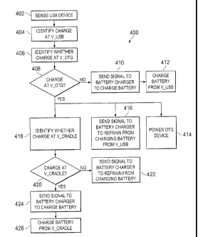
[0031] FIG. 4 is a process flow diagram 400 for charging an electronic device
and/or a
USB HOST MODE peripheral device connected to the electronic device. The
electronic device
can include a first charging port. The first charging port may be, for
example, a USB port or
other port that can receive a peripheral device either directly or through a
cable or by other ways.
The electronic device can sense whether a USB device (such as a USB charger or
USB HOST
MODE peripheral device) is connected to the first charging port of the
electronic device (402).
In certain instances, the electronic device can sense the USB device because,
for example, the
attachment of a USB device to the USB port can close a circuit between the
electronic device
and the USB device. The closed circuit can cause voltage across the closed
circuit to allow the
movement of charge between the electronic device and the USB device. This
movement of
charge may be sufficient to establish a signal to the electronic device that
the USB device is
connected to the electronic device.
[0032] The first charging port may include several pins or terminals
(generally,
terminals). The terminals can individually connect to terminals on the USB
device to complete
one or more circuits. In general, when a terminal of the first charging port
completes a circuit
with a terminal on the USB device, this interface can be referred to as a
"connection." A first
connection can complete a circuit between the USB device and a battery charger
of the electronic
device. A second connection can complete a circuit between the USB device and
a battery or a
PMIC of the electronic device. For example, if the USB device includes a USB
HOST MODE
peripheral device, the battery and/or PMIC from the electronic device can
power the USB HOST
11
CA 02815820 2013-05-08
MODE peripheral device. In some instances, one or both connections can be
completed. In
addition, one or both of the first and second connections can complete a
circuit with a bypass
circuit (or charger controller circuit). A completion of a circuit can allow
voltage to move
charge across a connection.
[0033] The first connection can include a terminal referred to as V USB. A
charge can
be identified at a first connection of the USB port (404). The charge can be
identified, for
example, because the existence of a circuit path based on a first connection
between V USB and
the USB device allows voltage to move charge across the first connection. In
general, the term
"identify" is meant to include different ways of sensing, determining,
detecting, or otherwise
identifying, in this case, that a charge exists at a connection. It can also
be identified whether
there is a charge at a second connection of the USB port (406). The second
connection can
include a terminal referred to as V_OTG (408). If there is a charge at the
first connection of the
USB port (406) and no charge at V_OTG, then the bypass circuit allows a signal
to be sent to the
battery charger to charge the battery (410), and the battery charger can
charge the battery (412).
[0034] If there is a charge at V_OTG (e.g., the USB device includes a USB HOST
MODE peripheral device, and the second connection completes a circuit between
a terminal of a
USB HOST MODE peripheral device (V_OTG) and a terminal of the first charging
port), the
electronic device can provide power to the USB HOST MODE peripheral device
(414). For
example, charge from the battery or PMIC of the electronic device can be
directed across the
second connection to the USB HOST MODE peripheral device. In addition, a
signal can be sent
to the battery charger (e.g., from the bypass circuit) to refrain from
charging the battery from the
connection that includes terminal V USB (416).
[0035] In certain implementations, a determination can be made (e.g., in
software) of
whether an USB HOST MODE peripheral device is connected. The previous
discussion
illustrates some techniques by which a processor or battery charger may
determine, through
voltage or signals, whether a peripheral device is electrically connected to a
port. In other
instances, the bypass circuit can operate based on the circuit elements and
without making a
determination. Specifically, a voltage at V_OTG may be an input voltage into
the circuit
element described in FIG. 3 (NFET 304). The NFET operates based on the
presence of a
threshold voltage at a gate terminal (V_OTG). A voltage at V_OTG that is
sufficiently high can
activate the transistor to pass current without the transistor having to make
a determination ¨ the
12
CA 02815820 2013-05-08
transist9r simply activates. A USB device connected to the first charging port
can close a circuit
for one or both of V_USB and V_OTG, which causes a voltage on V_USB and/or
V_OTG. If
the USB device is a USB charger, then there may be no voltage on V_OTG. If the
USB device
is a USB HOST MODE peripheral device, there may be a voltage on V_USB and
V_OTG. A
voltage at both terminals may cause the battery to try to charge itself. Thus,
V_USB and
V_OTG are connected to a bypass circuit. The bypass circuit can include a
circuit element that
can detect or sense a voltage at V_USB and at V_OTG. The circuit element may
be a transistor,
such as an NFET. V_OTG may be connected to the gate of the NFET, and V_USB can
be
connected to the drain of the NFET via a high resistance resistor. If there is
a voltage at V_OTG
that is sufficiently high, the NFET can activate, causing current to flow from
the drain to the
source of the NFET. By keeping the source of the NFET at ground, current will
flow through the
transistor to ground when the transistor is activated ¨ so when there is a
voltage on V_OTG and
V_USB, no charge flows out of the NFET into the rest of the bypass circuit
(see FIG. 3). This
lack of charge flow can establish a signal to the battery charger to refrain
from charging the
battery. If there is no voltage at V_OTG, the transistor acts as an open
circuit. Voltage at
V_USB can cause charge to flow out of the NFET and into the rest of the bypass
circuit,
signaling the battery charger to charge the battery (e.g., from V_USB).
[0036] A charge can be sensed at a second charging port which includes a
cradle terminal
(V_Cradle) (418). The second charging port can be an interface for a cradle
charging device or
other device. A third connection can be established by the interface between
V_Cradle and a
terminal on the cradle device. The third connection can establish a circuit
path between the
cradle device and elements of the electronic device, such as the battery
charger and/or bypass
circuit. When there is a voltage at the cradle port (420), a signal is sent to
the battery charger to
charge the battery (424). The battery can then be charged (426), i.e., the
battery charger supplies
or provides a charging current or voltage to the battery. If there is no
voltage at the cradle port
(420), a signal can be sent to the battery charger to refrain from charging
the battery (422). If no
charge is detected at the cradle port, the port can be considered "open" or an
"open circuit"
where there is no circuit connection between the cradle port and a cradle
device. Thus, no
charge is directed from the cradle device to the battery charger. In certain
implementations,
refraining from charging the battery includes directing the charge received at
the cradle port
away from the battery charger (e.g., so that the battery does not waste power
trying to charge
13
CA 02815820 2013-05-08
itself). ,The charge may be directed to, for example, other electronic
components in the host, or
the charge may be directed on or to the USB port (and thereby to a connected
peripheral device),
or both, or the charge may be directed nowhere (i.e., the absence of voltage
results in no charge
movement, or current). In certain instances, a determination can be made as to
whether there is a
voltage at the cradle port (and/or whether this voltage is associated with a
cradle). In other
implementations, the presence of a voltage at a cradle terminal (V Cradle)
will cause a bypass
circuit to signal the battery charger to charge the battery.
[0037] Several implementations have been described in detail above, and
various
modifications are possible. The disclosed subject matter, including the
functional operations
described in this specification, can be implemented in electronic circuitry,
computer hardware,
firmware, software, or in combinations of them, such as the structural means
disclosed in this
specification and structural equivalents thereof, including potentially a
program operable to
cause one or more data processing apparatus to perform the operations
described (such as a
program encoded in a computer-readable medium, which can be a memory device, a
storage
device, a machine-readable storage substrate, or other physical, machine-
readable medium, or a
combination of one or more of them). For example, NFET 304 of FIG. 3 connected
to V_USB
can be controlled by software. A "high" signal can restrict current from
flowing from V USB to
the battery charger 306, whereas a "low" signal will allow current to flow.
Alternatively,
software can disable charging by controlling the negative charge enable
terminal on the battery
charger 306.
[0038] While this specification contains many specifics, these should not be
construed as
limitations on the scope of what may be claimed, but rather as descriptions of
features that may
be specific to particular implementations. Certain features that are described
in this specification
in the context of separate implementations can also be implemented in
combination in a single
implementation. Conversely, various features that are described in the context
of a single
implementation can also be implemented in multiple implementations separately
or in any
suitable subcombination. Moreover, although features may be described above as
acting in
certain combinations and even initially claimed as such, one or more features
from a claimed
combination can in some cases be excised from the combination, and the claimed
combination
may be directed to a subcombination or variation of a subcombination.
14
CA 02815820 2015-07-14
[0039] Similarly, while operations are depicted in the drawings in a
particular order, this
should not be understood as requiring that such operations be performed in the
particular order
shown or in sequential order, or that all illustrated operations be performed,
to achieve desirable
results. In certain circumstances, multitasking and parallel processing may be
advantageous.
Moreover, the separation of various system components in the implementations
described above
should not be understood as requiring such separation in all implementations.
[0040] The features of above-described embodiments may give rise to one or
more
advantages. For example, aspects of the present disclosure allow for an
electronic device to
power a USB HOST MODE peripheral device without the battery of the electronic
device
sending charge to itself. Further, aspects of the present disclosure provide
for multiple charging
ports while maintaining a low-cost, compact design that operates relatively
quickly and, in some
implementations, automatically (i.e., without determinative steps or
instructions). The compact
design allows for smaller electronic devices and/or more room for other
features or circuits. It
will be understood by those having skill in the art that many changes may be
made to the details
of the above-described embodiments. The present invention may be embodied in
other specific
forms without departing from the subject matter of the claims. The described
example
embodiments are to be considered in all respects as being only illustrative
and not restrictive
unless otherwise stated. The scope of protection being sought is defined by
the following claims
rather than the described embodiments in the foregoing description. The scope
of the claims
should not be limited by the embodiments set forth in the examples, but should
be given the
broadest interpretation consistent with the description as a whole.