Note: Descriptions are shown in the official language in which they were submitted.
-1-
SWITCHING SYSTEMS AND METHODS FOR USE IN
UNINTERRUPTIBLE POWER SUPPLIES
RELATED APPLICATIONS
This application claims benefit of U.S. Provisional Patent Application
Serial No. 61/435,317 fired January 23, 2011.
TECHNICAL FIELD
The present invention relates the generation of a standby power signal
and, more specifically, to uninterruptible power supply systems and methods
that generate a standby signal using an inverter system.
BACKGROUND
Uninterruptible power supplies (UPS's) have long been used to provide
at least temporary auxiliary power to electronic devices. Typically, a UPS is
configured to switch between a primary power source and a standby power
source as necessary to maintain constant power to a load. Typically, the
primary power source for a UPS is a utility power supply, and the standby
power source may take the form of a battery system. The UPS will normally
operate in a line mode in which the utility power signal is passed to the load
when the utility power signal is within predefined parameters. In the line
mode, the UPS will typically also charge the battery system. When the utility
CA 2825483 2018-05-29
;A 02825483 2013 07 18
WO 2012/148512 PCT/US2012/021619
-2-
power falls outside of the predefined parameters, the UPS will switch to
standby mode in which an AC signal is generated based on the energy stored
in the battery system.
A class of UPS's employs a ferroresonant transformer. A
ferroresonant transformer is a saturating transformer that employs a tank
circuit comprised of a resonant winding and capacitor to produce a nearly
constant average output even if the input to the transformer varies. A typical
UPS employing a ferroresonant transformer takes advantage of the voltage
regulating properties of a ferroresonant transformer in both line and standby
to modes. In the context of a UPS, a ferroresonant transformer thus
provides
surge suppression, isolation, short circuit protection, and voltage regulation
without the use of active components.
Conventionally, in line mode, a UPS employs an inverter circuit
configured to form a switch mode power supply. An inverter circuit configured
as a switch mode power supply typically comprises at least one and typically
a plurality of power switches that are operated according to a pulse-width
modulated (PWM) signal. The PWM method of generating an AC signal from
a DC source allows the amplitude of the AC signal to be determined at any
point in time by controlling the duty cycle at which the inverter power
switches
are operated. Controlling the duty cycle at which the inverter power switches
are operated produces, through an output LC filter, a desired net average
voltage. Typically, the parameters of the inverter control signal are varied
according to a control signal generated by a feedback loop having an input
formed by at least one characteristic, such as voltage, of the AC signal.
In a switch mode power supply, one of the major causes of loss of
efficiency arises from the imperfect switching characteristics of modern power
switches during the transition between the ON and OFF configurations of the
power switches. An object of the present invention is to provide switch mode
power supplies for use in UPS systems having improved efficiency.
;A 02825483 2013 07 18
WO 2012/148512 PCT/US2012/021619
-3-
SUMMARY
The present invention may be embodied as an uninterruptible power
supply for providing an output power signal to a load based on an input power
signal comprising an input section, an output section, an inverter section,
and
a transformer. The input section is operatively connected to the input power
signal. The output section is operatively connected to the load. The inverter
section is operatively connected to an alternative power source. The
transformer is operatively connected to the input section, the output section,
and the inverter section. The uninterruptible power supply operates in a line
mode and in a standby mode. In the line mode, the output section generates
the output power signal based on the input power signal. In the standby
mode, the output section generates the output power signal from a standby
signal generated by the inverter section based on the alternative power
source and at least one inverter control signal. When the uninterruptible
power supply operates in the standby mode, the at least one inverter control
signal is pulse-width modulated during at least a first portion of a cycle of
the
output power signal and not pulse-width modulated during at least a second
portion of the cycle of the output power signal.
The present invention may also be implemented as a method of
providing an output power signal to a load based on an input power signal
comprising the following steps. An input section is connected to the input
power signal. An output section is connected to the load. An inverter section
is connected to an alternative power source. A transformer is connected to
the input section, the output section, and the inverter section. The
uninterruptible power supply is operated in a line mode and a standby mode.
In the line mode, the output generates the output power signal based on the
input power signal. In the standby mode, the output section generates the
;A 028254832013-07-18
WO 2012/148512 PCT/US2012/021619
-4-
output power signal based on a standby signal generated by the inverter
section from the alternative power source and at least one inverter control
signal. When the uninterruptible power supply operates in the standby mode,
the at least one inverter control signal is generated such that the at least
one
inverter control signal is pulse-width modulated during at least a first
portion
of a cycle of the output power signal and not pulse-width modulated during at
least a second portion of the cycle of the output power signal.
The present invention may also be embodied as an uninterruptible
power supply for providing an output power signal to a load based on an input
power signal comprising an input section, an output section, an inverter
section, and a transformer. The input section is operatively connected to the
input power signal. The output section is operatively connected to the load.
The inverter section is operatively connected to an alternative power source.
The transformer is operatively connected to the input section, the output
section, and the inverter section. The uninterruptible power supply operates
in a line mode and in a standby mode. In the line mode, the output section
generates the output power signal based on the input power signal. In the
standby mode, the output section generates the output power signal from a
standby signal generated by the inverter section based on the alternative
power source and first and second inverter control signals. When the
uninterruptible power supply operates in the standby mode, the first inverter
control signal is
switched between OFF and ON states during a first portion of the cycle of the
output power signal, held in the ON state during a second portion of the cycle
of the output power signal, switched between OFF and ON states during a
third portion of the cycle of the output power signal. When the
uninterruptible
power supply operates in the standby mode, the second inverter control
signal is switched between OFF and ON states during a fourth portion of the
cycle of the output power signal, held in the ON state during a fifth portion
of
- 5 -
the cycle of the output power signal, and switched between OFF and ON states
during a
sixth portion of the cycle of the output power signal.
In a broad aspect, the invention pertains to an uninterruptible power supply
for
providing an output power signal to a load based on an input power signal
comprising, an
input section operatively connected to the input power signal, an output
section
operatively connected to an alternative power source, and a transformer
operatively
connected to the input section, the output section, and the inverter section.
The
uninterruptible power supply operates in a line mode in which the output
section
generates the output power signal based on the input power signal, and a
standby mode in
which the output section generates the output power signal from a standby
signal is
generated by the inverter section based on the alternative power source and at
least one
inverter control signal. The output power is a quasi square wave having a
first change of
phase, an upper limit, and a second change of phase. A cycle of the output
power signal
comprises a first portion, a second portion, and a third portion, in which the
first portion
extends from the first change of phase to the upper limit, the third portion
extends from
the upper limit to the second change of phase, and the second portion extends
between
the first portion and the third portion. When the uninterruptible power supply
operates in
the standby mode, the at least one inverter control signal is pulse-width
modulated during
the first portion of a cycle of the output power signal, is held in an ON
state during the
second portion of the cycle of the output power signal, and is pulse-width
modulated
during the third portion of the cycle of the output power signal.
In a further aspect the invention embodies a method of providing an output
signal
to a load based on an input power signal comprising the steps of connecting an
input
section to the input power signal, connecting an output section to the load,
connecting an
inverter section to an alternative power source, and connecting a transformer
to the input
section, the output section, and the inverter section. The uninterruptible
power supply
operates in a line mode in which the output generates the output power signal
based on
the input power signal, and a standby mode in which the output section
generates the
output power signal, based on a standby signal generated by the inverter
section from the
CA 2825483 2018-05-29
=
- 5a -
alternative power source and at least one inverter control signal. When the
uninternIptible power supply operates in the standby mode, the at least one
inverter
control signal is generated such that the output power signal is a quasi
square wave
having a first change of phase, an upper limit, and a second change of phase.
A cycle of
the output power signal comprises a first portion, a second portion, and a
third portion, in
which the first portion extends from the first change of phase to the upper
limit, the third
portion extends from the upper limit to the second change of phase, and the
second
portion extends between the first portion and the third portion. The at least
one inverter
control signal is pulse-width modulated during the first and third portions of
the cycle of
the output power signal, and is held in an ON state during the second portion
of the cycle
of the output power signal.
Still further, the invention provides an uninterruptible power supply for
providing
an output power signal to a load comprising a ferroresonant transformer, a
resonant
capacitor operatively connected to the ferroresonant transformer, and an
inverter
operatively connected to the ferroresonant transformer. The inverter is
configured to
generate the output power signal based on at least one inverter control signal
such that the
output power signal is a quasi square wave having a first change of phase, an
upper limit,
and a second change of phase. The at least one inverter control signal is
pulse-width
modulated between the first change of phase and the upper limit, pulse-width
modulated
between the upper limit and the second change of phase, and held in an ON
state when
the output power signal is at the upper limit.
Yet further, the invention offers a method of providing an output power signal
to
a load comprising providing a ferroresonant transformer, operatively
connecting a
resonant capacitor to the ferroresonant transformer, and operatively
connecting an
inverter to the ferroresonant transformer. At least one inverter control
signal is supplied
to the inverter such that the output power signal is a quasi square wave
having a first
change of phase, an upper limit, and a second change of phase. The at least
one inverter
CA 2825483 2018-05-29
=
- 5b -
control signal is pulse-width modulated between the first change of phase and
the upper
limit, and the at least one inverter control signal is pulse-width modulated
between the
upper limit and the second change of phase. The at least one inverter control
signal is
held in an ON state when the output power signal is at the upper limit.
DESCRIPTION OF THE DRAWINGS
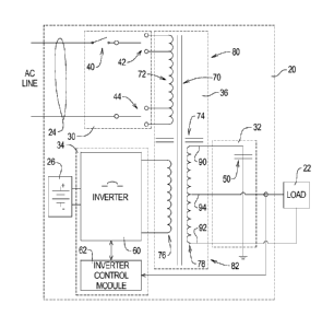
FIG. 1 is a simplified block diagram of a first embodiment of an
uninterruptible
power supply system using a ferroresonant transformer system constructed in
accordance
with, and embodying, the principles of the present invention;
FIG. 2 is a timing diagram representing control and power signals employed by
the UPS system depicted in FIG. 1; and
FIG. 3 depicts a first quasi-square wave form,, a second quasi-square wave
form,
and a third quasi-square waveform.
CA 2825483 2018-05-29
;A 02825483 2013 07 18
WO 2012/148512 PCT/US2012/021619
-6-
DETAILED DESCRIPTION
Referring initially to FIG. 1 of the drawing, depicted therein is a first
example of an uninterruptible power supply (UPS) system 20 constructed in
accordance with, and embodying, the principles of the present invention. The
present invention is of particular significance when applied to a UPS system
adapted for use in a communications system, such as CATV or telephony
system, and that use of the present invention will be disclosed herein in
detail.
However, it should be understood that the principles of the present invention
may be applied to UPS systems adapted for use in environments other than
communications systems.
The example UPS system 20 supplies power to a load 22 based on a
primary power signal present on an AC power line 24 (line mode) or a
secondary power signal generated by a battery pack 26 (standby mode).
While the example secondary power signal is generated by a battery pack in
the example UPS system 20, alternative power sources such as generators,
fuel cells, solar cells, and the like may be used as the secondary power
source.
The example UPS system 20 comprises an input section 30, an output
section 32, an inverter section 34, and a ferroresonant transformer 36. The
example input section 30 comprises a main switch 40 and first and second
select switches 42 and 44. The example output section 32 comprises an
output (e.g., resonant) capacitor 50. The output capacitor 50 forms a
resonant or tank circuit with the transformer 36 as will be described in
further
detail below.
The inverter section 34 comprises an inverter circuit 60 and a controller
62. The inverter circuit 60 may be an H-bridge circuit or any other circuit
capable of producing an appropriate AC power signal based on a DC power
-7-
signal obtained from the battery pack 26. The inverter circuit 60 is or may be
conventional and will not be described herein in further detail.
The example controller 62 controls the inverter circuit 60. The
controller 62 may further control the charging of the battery pack 26 when the
UPS system 20 operates in line mode based on temperature, voltage, and/or
current signals associated with the battery pack 26.
The example inverter circuit 60 is pulse-width modulated, and the
inverter section 34 functions as a switch mode power supply when the UPS
system operates in the standby mode. As will be described in further detail
below, the controller 62 generates one or more inverter control signals that
control the inverter circuit to generate a switched output signal.
The example ferroresonant transformer 36 comprises a core 70, input
windings 72, an inductor 74, inverter windings 76, and output windings 78.
The core 70 is or may be a conventional laminate structure. The inductor 74
defines a primary side 80 and a secondary side 82 of the transformer 36. In
the example UPS system 20, the output capacitor 50 is connected across first
and second ends 90 and 92 of the output windings 78, and the load is
connected between the second end 92 of the output windings 78 and a tap 94
in the output windings 78.
In the example transformer 36, only the input windings 72 are on the
primary side 80 of the transformer 36. The inverter windings 76 and output
windings 78 are on the secondary side 82 of the transformer 36. In particular,
the output windings 78 are arranged between the inverter windings 76 and
the inductor 74, and the inductor 74 is arranged between the output windings
78 and the input windings 72. A ferroresonant transformer appropriate for
use as the example ferroresonant transformer 36 is described, for example, in
US. Patent publication No. 2011/0198932, and this publication may
be referred to for further details. The principles of the present invention
may, however, be applied to other configurations of
CA 2825483 2018-05-29
;A 028254832013-07-18
WO 2012/148512 PCT/US2012/021619
-8-
ferroresonant transformers.
In line mode, the main switch 40 is closed and the AC power line 24 is
present on the input windings 72. The input windings 72 are
electromagnetically coupled to the output windings 78 such that a primary AC
output signal is supplied to the load 22 when the UPS system 20 operates in
the line mode.
In standby mode, the main switch 40 is opened, and the battery pack
26 and inverter section 34 form a secondary power source supplies a standby
AC output signal to the load 22. In particular, in standby mode the inverter
section 34 generates the switched power signal across the inverter windings
76, and the inverter windings 76 are electromagnetically coupled to the output
windings 78 and to the output capacitor such that the standby AC output
signal is present across the tap 94 and the second end 92 of the output
windings 78. Further, during standby mode, an optional switch (not shown)
may be provided in series with the output capacitor 50 to allow the output
capacitor 50 to be disconnected from the output windings, thereby reducing
peak inverter currents observed due to charging and discharging of the output
capacitor 50.
The example inverter section 34 conventionally comprises at a plurality
of power switches (not shown) configured as a switch mode power supply.
Typically, the power switches are MOSFETS configured as an H-bridge circuit
or any other circuit capable of producing an appropriate standby AC power
signal based on a DC power signal obtained from the battery pack 26.
The inverter control module 62 generates one or more inverter control
signals based on a characteristic, such as voltage, of the standby AC output
signal applied to the load 22. The inverter control signal or signals may be
pulse-width modulated (PWM) signals the characteristics of which cause the
power switches of the inverter circuit 60 to open and close as necessary to
generate the standby AC output signal within predetermined voltage,
;A 02825483 2013 07 18
WO 2012/148512 PCT/US2012/021619
-9-
frequency, and waveform parameters. In the example UPS system 20
operating in standby mode, the inverter circuit 60, inverter control circuit
62,
the inverter windings 76, and output windings 78 thus form a feedback loop
that controls a desired net average voltage as appropriate for the load 22.
The Applicants have recognized that loads, such as the example load
22 to which power is supplied by a UPS used in communications networks
such as CATV networks, are constant power loads that typically employ a
diode rectifier circuit supplying a large capacitor bank. Such loads demand
very high current at the peak AC power voltage at the instant the AC voltage
amplitude exceeds the bus capacitor voltage. The Applicants further
recognized that a substantial portion, if not all, of the load power will be
delivered in the period during which the AC voltage amplitude is higher than
the DC bus capacitor. This results in higher peak current to compensate for
the fact that less than 100% of the time is available to transfer energy to
the
load.
The inverter control module 62 of the present invention thus eliminates
the pulse-width modulation at the peak of the standby AC output signal. The
Applicant has discovered that the elimination of pulse-width modulation at the
peak of the standby AC output signal allows the power switches of the
inverter circuit 60 to be full ON (100% duty cycle) during the time of peak
current transfer to the bus capacitors. Eliminating pulse-width modulation of
the inverter control signal during at least part of the cycle of the standby
AC
output signal significantly improves (by between approximately 10-20%) the
efficiency of the UPS system 20 when operating in standby mode.
Referring now to FIG. 2 of the drawing, depicted therein are several
waveforms that may be implemented by the example UPS system 20
operating in standby mode. FIG. 2 conventionally plots each voltage (y-axis)
versus time (x-axis). FIG. 2 is further divided into first through ninth time
periods T1.9 separated by vertical broken lines.
;A 028254832013-07-18
WO 2012/148512 PCT/US2012/021619
-10-
Depicted at 120 is an example standby AC output signal 120 supplied
to the load 22. Depicted at 130 in FIG. 2 is an example switched power
signal 130 generated by the inverter section 34 and applied across the
inverter windings 76. Depicted at 140 and 142 in FIG. 2 are representations
of inverter control signals that may be generated by the inverter control
module 62 for controlling the inverter power switches of the inverter circuit
60.
As is conventional, the first inverter control signal using the principles of
the
present invention, the inverter control signals 140 and 142 may operate at a
relatively high frequency, e.g., approximate 20kHz, with a duty cycle that is
varied between 0% and 100% as described below to obtain the desired
waveform.
The period of peak current transfer occurs in the time periods T2, T53
and T8 in FIG. 2. During these periods, the inverter control signal generated
by the inverter control module 62 for controlling the inverter circuit 60 is
held
in a state that closes the power switches (100% duty cycle) of the inverter
circuit 60. FIG. 2 further shows that the switched power signai 130 generated
by the example inverter section 34 is pulse-width modulated (switched
between OFF and ON) during the time periods T1, T3, T4, T6, T7 and Tg
outside of the periods of peak current transfer and is held HIGH (100% duty
cycle) during the time periods T2, T5, and T8. The operation of these switches
of the inverter circuit 60 in their least efficient mode (from ON to OFF or
from
OFF to ON) is thus avoided during the period of peak current transfer to the
load 22. The inverter control signals 140 and 142 represent one example
method of controlling an inverter circuit such as the example inverter circuit
60 to generate the switched power signal 130 and standby AC output signal
120 as depicted in FIG. 2
The example standby AC output signal 120 depicted in FIG. 2 is what
is referred to as a modified or quasi square wave. A standby AC power signal
having a modified or quasi square wave, such as the example signal 120, is
;A 02825483 2013 07 18
WO 2012/148512
PCT/US2012/021619
-11-
appropriate for providing power to the load 22.
To provide voltage regulation, the duration of the periods of time T2, 15,
and T8 in which the switches are operated at 100% duty cycle (held ON) can
be varied as shown in FIG. 3. FIG. 3 illustrates second and third example
standby AC power signals 150 and 160; the example standby AC power
signal 120 is also reproduced in FIG. 3 for reference. The second example
standby AC power signal 150 corresponds to a load having a low DC bus
relative to the mid DC bus of the load corresponding to the first example
standby AC output signal 120. The third example standby AC power signal
160 corresponds to a load having a high DC bus relative to the mid DC bus of
the load corresponding to the first example standby AC output signal 120.
Additionally, to provide voltage regulation and maintain an acceptable
modified or quasi square wave, the inverter control signals 140 and 142 are
generated to alter the dVidt, or slope, of the standby AC power signal 120
during the time periods Ti, T3, T4, Ts, T7 and Tg outside of the periods of
peak
current transfer. Additionally, the switched power signal 130 may be held at
zero during phase change transitions to allow more control of voltage
regulation.
The second example standby AC power signal 150 thus has a lower
peak voltage during peak current transfer in the time periods T2, T5, and T8
and steeper slope during the time periods T1, T3, 14, T6, T7 and T9 outside of
the periods of peak current transfer. The steeper slope in the time periods
Ti,
T3, T4, 16, T7 and Tg is obtained by appropriate control of the duty cycle of
the
switched power signal 130.
The third example standby AC power signal 160, on the other hand,
has a higher peak voltage during peak current transfer in the time periods T21
T5, and T8. The slope of the third example standby AC power signal is similar
to the slope of the first example AC power signal 160 during the time periods
Ti, T3, T4, T6, T7 and Tg outside of the periods of peak current transfer.
;A 028254832013-07-18
WO 2012/148512 PCT/US2012/021619
-12-
However, the third example standby AC power signal 160 is held at zero for a
short time during crossover periods 162 and 164 when the AC power signal
160 changes phase. The zero voltage at the crossover periods 162 and 164
is obtained by turning the switched power signal 130 OFF (0% duty cycle)
during the crossover periods 162 and 164.
More generally, the switching pattern of the inverter control signals and
the design of the transformer are optimized to provide maximum efficiency
across the specified output voltage and specified load range. Relevant
optimization schemes include providing enough volt-seconds to the inverter
winding to meet the voltage requirements of the load but not so many volt-
seconds that the transformer saturates.
Given the foregoing, it should be apparent that the principles of the
present invention may be embodied in forms other than those described
above. The scope of the present invention should thus be determined by the
claims to be appended hereto and not the foregoing detailed description of
the invention.