Note: Descriptions are shown in the official language in which they were submitted.
CA 2840244 2017-05-30
SYSTEM FOR LIGHTING APPARATUS UTILIZING LIGHT ACTIVE SHEET
MATERIAL WITH INTEGRATED LIGHT EMITTING DIODE, WINDOW WITH
LIGHTING APPARATUS, CONVEYANCE WITH LIGHTING APPARATUS, AND
METHOD OF PROVIDING LIGHTING APPARATUS
CROSS-REFERENCE TO RELATED APPLICATIONS
[0001] This application claims the benefit of U.S. Provisional Application
No. 61/512,272
filed July 27, 2011.
TECHNICAL FIELD
[0002] The technical field relates in general to light sources, and more
specifically to light
sources utilizing a transparent and non-transparent light active sheet
material, optionally for
conveyances.
BACKGROUND
[0003] In the vehicle lighting industry, illumination can be achieved
through the use of
various light sources, all of which require a housing, a substrate, or a body
composed of a
material through which light can pass. Therefore, conventional lamps for
illumination must be
mounted in areas that do not restrict vision or light.
[0004] This disclosure assumes that the reader has familiarity with US
7,217,956, titled
"LIGHT ACTIVE SHEET MATERIAL" sometimes referred to herein as "light sheet" or
"light
sheet technology," and with US 2008/0079012, titled "ILLUMINATED DEVICES
UTILIZING
TRANSPARENT LIGHT ACTIVE SHEET MATERIAL WITH INTEGRATED LIGIIT
EMITTING DIODE (LED), METHODS AND KIT THEREFOR".
[0005] Alternative solutions for a flexible thin light product that can be
used as either an
edge or flat light product that presently exist include:
Light pipe ¨ one disadvantage is its non-uniformity around corners
EL lighting ¨ one disadvantage is EMI concerns created with DC/DC converter
OLED ¨ one disadvantage is that it can degrade when exposed to humidity and
can be difficult to seal from exterior environment.
SUMMARY
[0006] Preliminarily, it may be noted that features of various embodiments
discussed herein
may be combined with other features and/or with other embodiments discussed
herein.
[0007] First Embodiment
CA 02840244 2013-12-20
WO 2013/016646
PCT/US2012/048569
[0008] Accordingly, one or more embodiments is a method of providing edge
lighting. A
lighting device is provided; the lighting device has at least one light
emitting diode (LED)
chip embedded therein, wherein the at least one LED chip generates light
photons. A path of
the light photons within the lighting device that are emitted by the at least
one LED chip from
a top surface of said at least one LED chip, is redirected from a first edge
of the lighting
device back through the lighting device to a second edge of the lighting
device opposite to the
first edge, the first edge and the second edge being perpendicular to the top
surface of said at
least one LED chip. The photons which were redirected from the first edge of
the lighting
device are transmitted in a path through the second edge of the device and
then being output
from the lighting device at the second edge of the device.
[0009] In one or more embodiments, the lighting device comprises a unitary
structure of
at least two substrates sandwiching the at least one LED chip.
[0010] In another embodiment, a metalized film is provided on the first
edge of the
lighting device, wherein the metalized film redirects the path of the light
photons back
emitted from the at least one LED chip back through the lighting device toward
the second
edge.
[0011] In yet another embodiment, a laser cut finish is provided on the
first edge of the
lighting device, wherein the laser cut finish redirects the path of the light
photons emitted
from the at least one LED chip back through the lighting device toward the
second edge.
[0012] In still another embodiment, a laser etch mark is provided on a
surface of a
substrate forming the lighting device, the laser etch mark being positioned to
intercept the
light photons emitted from the at least one LED chip toward the surface of the
substrate and
to couple the intercepted light photons to the second edge of the lighting
device. In a further
embodiment, a metalized film is provided on a surface of a substrate forming
the lighting
device, the metalized film being positioned to intercept the light photons
emitted from the at
least one LED chip toward the surface of the substrate and to couple the
intercepted light
photons to the second edge of the lighting device.
[0013] In yet a further embodiment, a plurality of the lighting devices are
provided in one
single assembly in a sandwich structure, at least one of the lighting device
emitting light in a
color different from light emitted by others of the plurality of the lighting
devices, each of the
lighting devices being individually selectable to provide selectable colored
lighting.
In still a further embodiment, the second edge of the lighting device has a
width of 5 mm or
2
CA 02840244 2013-12-20
WO 2013/016646
PCT/US2012/048569
less, wherein light which is output at the second edge and which includes the
light photons
which were redirected from the first edge of the lighting device provides an
appearance of a
substantially continuous ribbon of light having a width of 5 mm or less along
the second
edge.
In another embodiment, the lighting device comprises at least one optically
transparent
electrically conductive substrate that sandwiches the at least one LED chip,
the first and
second edges being formed on the transparent electrically conductive
substrate, the light
photons being emitted from the at least one LED chip through the optically
transparent
electrically conductive substrate.
[0014] In still another embodiment, the lighting device includes a
transparent light active
sheet material, the transparent light active sheet material comprises top and
bottom
electrically conductive transparent substrates, a pattern of LED chips
sandwiched between the
electrically conductive transparent substrates, and a non-conductive
transparent adhesive
material disposed between the top and bottom electrically conductive
transparent substrates
and the LED chips. The LED chips are preformed before being patterned in the
light active
sheet material as an unpackaged discrete semiconductor device having an anode
p-junction
side and a cathode n-junction side. Either of the anode and the cathode side
is in electrical
communication with one of the electrically conductive transparent substrates,
and the other of
the anode and the cathode side is in electrical communication with the other
of the
electrically conductive transparent substrates.
[0015] In still a further embodiment, the at least one LED chip is disposed
in the lighting
device and the second edge to be separated by a predetermined distance, to
provide a
predetermined brightness and diffused appearance on the second edge.
[0016] In another embodiment, the at least one LED chip is a plurality of
LED chips that
generate the light photons, the plurality of LED chips being linearly disposed
in the lighting
device parallel to at least one of the first and second edges.
[0017] Also, an embodiment is a method of providing a conveyance with edge
lighting.
Edge lighting is provided. The edge lighting is mounted on the conveyance. The
edge
lighting is electrically connected to an electrical wiring harness of the
conveyance.
[0018] In another embodiment, the edge lighting is arranged within a
designed gap
between trim pieces of the conveyance.
3
CA 02840244 2013-12-20
WO 2013/016646
PCT/US2012/048569
[0019] In yet another embodiment, the edge lighting is arranged to bend the
second edge
of the lighting device to have a radius.
[0020] According to another embodiment, there is an edge lighting
apparatus. The edge
lighting apparatus includes a lighting device with at least one light emitting
diode (LED) chip
embedded therein, wherein the at least one LED chip generates light photons. A
path of the
light photons within the lighting device that are emitted by the at least one
LED chip from a
top surface of said at least one LED chip, being redirected from a first edge
of the lighting
device back through the lighting device to a second edge of the lighting
device opposite to the
first edge, the first edge and the second edge being perpendicular to the top
surface of said at
least one LED chip, the photons which were redirected from the first edge of
the lighting
device being transmitted in a path through the second edge of the device and
then being
output from the lighting device at the second edge of the device.
[0021] Yet another embodiment is a method of making an edge lighting
apparatus. The
method includes providing a lighting device with at least one light emitting
diode (LED) chip
embedded therein, wherein the at least one LED chip generates light photons
when powered,
the lighting device having a first edge and a second edge which is opposite to
the first edge.
The method also includes treating at least one of the first edge and the
second edge, so that
the second edge is more transmissive of the light photons than the first edge,
and the first
edge redirects a path of the light photons within the lighting device that are
emitted by the at
least one LED chip from a top surface of said at least one LED chip, from the
first edge of the
lighting device back through the lighting device to a second edge of the
lighting device
opposite to the first edge, the first edge and the second edge being
perpendicular to the top
surface of said at least one LED chip, the photons which were redirected from
the first edge
of the lighting device being transmitted in a path through the second edge of
the device and
then being output from the lighting device at the second edge of the device.
[0022] Second Embodiment
[0023] One or more embodiments provides a dual lighting apparatus. The dual
lighting
apparatus includes a principal substrate; a first lighting device integrated
into a first plane of
the principal substrate, the first lighting device having at least one first
light emitting diode
(LED) chip embedded therein; and a second lighting device integrated into a
second plane of
the principal substrate, the second lighting device having at least one second
light emitting
diode (LED) chip embedded therein. The at least one first LED chip emits light
photons
4
CA 02840244 2013-12-20
WO 2013/016646
PCT/US2012/048569
having a different wavelength than light photons emitted from the at least one
second LED
chip.
[0024] In another embodiment, each of the first and second lighting devices
comprises a
unitary structure of at least two substrates sandwiching the at least one
first or second LED
chip.
[0025] In still another embodiment, each of the first and second lighting
devices
comprises at least one optically transparent electrically conductive substrate
that sandwiches
the at least one first or second LED chip, the light photons being emitted
from the at least one
first or second LED chip through the optically transparent electrically
conductive substrate.
[0026] In yet another embodiment, at least one of the first and second
lighting devices is
a transparent light active sheet material; the transparent light active sheet
material comprises
top and bottom electrically conductive transparent substrates, a pattern of
LED chips
sandwiched between the electrically conductive transparent substrates, and a
non-conductive
transparent adhesive material disposed between the top and bottom electrically
conductive
transparent substrates and the LED chips; the LED chips are preformed before
being
patterned in the light active sheet material as an unpackaged discrete
semiconductor device
having an anode p-junction side and a cathode n-junction side; and either of
the anode and the
cathode side is in electrical communication with one of the electrically
conductive transparent
substrates and the other of the anode and the cathode side is in electrical
communication with
the other of the electrically conductive transparent substrates.
[0027] In a further embodiment, the first and second planes of the
principal substrate are
disposed on opposite sides of the principal substrate.
[0028] In still another embodiment, the first and second lighting devices
are disposed on
different surfaces of a same plane of the principal substrate.
[0029] In yet another embodiment, the first and second planes of the
principal substrate
are disposed on different planes of the principal substrate.
[0030] In another embodiment, the first and second lighting devices are
configured to be
individually selectable to be powered on or off.
[0031] Another embodiment further incorporates a flexible electronic
circuit.
[0032] Another embodiment is a conveyance with dual lighting, and a method
for
providing same. The conveyance with dual lighting includes the dual lighting
apparatus
CA 02840244 2013-12-20
WO 2013/016646
PCT/US2012/048569
mounted on the conveyance, the dual lighting apparatus being electrically
connected to an
electrical wiring harness of the conveyance.
[0033] Yet a further embodiment is window with incorporated lighting
device. The
window includes a lighting apparatus, having: a principal substrate; a
lighting device
integrated into a plane of the principal substrate, the lighting device having
at least one light
emitting diode (LED) chip embedded therein; and plural glass substrates that
form the
window. The lighting apparatus is sandwiched between plural glass substrates
that form the
window and laminated therebetween.
[0034] A method of providing dual lighting is also disclosed. The method
includes
providing a principal substrate; integrating a first lighting device into a
first plane of the
principal substrate, the first lighting device having at least one first light
emitting diode
(LED) chip embedded therein; and integrating a second lighting device
integrated into a
second plane of the principal substrate, the second lighting device having at
least one second
light emitting diode (LED) chip embedded therein. The at least one first LED
chip emits
light photons having a different wavelength than light photons emitted from
the at least one
second LED chip.
[0035] Furthermore, a method of providing a window with incorporated
lighting device
includes laminating the lighting apparatus, sandwiched between plural glass
substrates that
form the window.
[0036] According to another embodiment, a method of providing a conveyance
with low
profile integrated lighting includes providing a lighting apparatus, the
lighting apparatus
comprising a substrate and a lighting device integrated into the substrate,
the lighting device
having at least one light emitting diode (LED) chip embedded therein, the
lighting device
further comprising an integrated flexible electronic circuit integrated into
the lighting device.
The lighting apparatus is mounted on a portion of an interior or exterior
surface of the
conveyance so that the substrate is substantially parallel to and in
continuous contact with the
interior or exterior surface of the conveyance, an electrical connection
powering the lighting
apparatus extending along the interior or exterior surface, and a profile of
the lighting
apparatus being less than 1 inch.
[0037] According to an embodiment, the profile of the lighting apparatus is
less than 0.2
inch.
[0038] Third Embodiment
6
CA 02840244 2013-12-20
WO 2013/016646
PCT/US2012/048569
[0039] According to an embodiment, a light source includes a substrate
arranged into at
least two facing surfaces which form a seam therebetween; and a lighting
device with a
plurality of light emitting diode (LED) chips embedded therein in a linear
arrangement,
wherein the plurality of LED chips generates light photons; the lighting
device has a first
edge and a second edge opposite to the first edge, the light photons within
the lighting device
that are emitted by the plurality of LED chips from a top surface of said LED
chips being
output from the lighting device at the second edge of the device; the lighting
device being
sandwiched in the seam between the two facing surfaces, the second edge of the
lighting
device being exposed when the seam is in an opened position. Also provided is
a method of
making the same.
[0040] In another embodiment, the lighting device comprises at least one
optically
transparent electrically conductive substrate that sandwiches the plurality of
LED chips, the
second edge being formed on the transparent electrically conductive substrate,
the light
photons being emitted from the plurality of LED chips through the optically
transparent
electrically conductive substrate.
[0041] In another embodiment, the substrate is a fabric material.
[0042] In yet another embodiment, there are included stitches through the
lighting device
and the substrate that attach the two facing surfaces to form the seam.
[0043] In still another embodiment, the substrate is arranged to cover an
interior surface
of a passenger compartment of a conveyance, the lighting device being disposed
to be
electrically connected to an electrical wiring harness of the conveyance.
[0044] In still another embodiment, the second edge of the lighting device
has a width of
mm or less, and light which is output at the second edge provides an
appearance of a
substantially continuous ribbon of light having a width of 5 mm or less along
the second
edge.
[0045] In another embodiment, the plurality of LED chips in the lighting
device and the
second edge as disposed to be separated by a predetermined distance, to
provide a
predetermined brightness and diffused appearance on the second edge.
[0046] In yet another embodiment, the second edge of the lighting device is
disposed
linearly along and parallel to the seam.
[0047] In still another embodiment, a path of the light photons within the
lighting device
that are emitted by the plurality of LED chips from the top surface of said
LED chips, is
7
CA 02840244 2013-12-20
WO 2013/016646
PCT/US2012/048569
redirected from the first edge of the lighting device back through the
lighting device to the
second edge of the lighting device, the first edge and the second edge being
perpendicular to
the top surface of said LED chips, the photons which were redirected from the
first edge of
the lighting device being transmitted in a path through the second edge of the
device and then
being output from the lighting device at the second edge of the device.
[0048] According to an embodiment, the lighting device is a transparent
light active sheet
material; the transparent light active sheet material comprises top and bottom
electrically
conductive transparent substrates, a pattern of the plurality of LED chips
sandwiched
between the electrically conductive transparent substrates, and a non-
conductive transparent
adhesive material disposed between the top and bottom electrically conductive
transparent
substrates and the plurality of LED chips; the plurality of LED chips are
preformed before
being patterned in the light active sheet material as an unpackaged discrete
semiconductor
device having an anode p-junction side and a cathode n-junction side; and
either of the anode
and the cathode side is in electrical communication with one of the
electrically conductive
transparent substrates and the other of the anode and the cathode side is in
electrical
communication with the other of the electrically conductive transparent
substrates.
[0049] Another embodiment provides a light source for use in an interior
surface of a
passenger compartment of a conveyance. The light source includes a lighting
device, the
lighting device has a plurality of light emitting diode (LED) chips embedded
therein, the
lighting device further includes an integrated flexible electronic circuit
integrated into the
lighting device, the lighting device is configured to be mounted on the
interior surface of the
conveyance, a profile of the lighting device is less than 1 inch, the lighting
device comprises
a unitary structure of at least first and second substrates sandwiching the
plurality of LED
chips; and a third substrate, the third substrate is arranged to cover the
lighting device on the
interior surface of the passenger compartment of the conveyance. The lighting
device is
disposed to be electrically connected to an electrical wiring harness of the
conveyance.
[0050] In an embodiment, the third substrate is a fabric material with
interwoven
conductors.
[0051] In another embodiment, the interior surface of the passenger
compartment is on a
passenger seat of the conveyance.
[0052] Further, the purpose of the foregoing abstract is to enable the U.S.
Patent and
Trademark Office and the public generally, and especially the scientists,
engineers and
8
CA 02840244 2013-12-20
WO 2013/016646
PCT/US2012/048569
practitioners in the art who are not familiar with patent or legal terms or
phraseology, to
determine quickly from a cursory inspection the nature and essence of the
technical
disclosure of the application. The abstract is neither intended to define the
invention of the
application, which is measured by the claims, nor is it intended to be
limiting as to the scope
of the invention in any way.
BRIEF DESCRIPTION OF THE DRAWINGS
[0053] The accompanying figures, drawings and/or photographs, where like
reference
numerals refer to identical or functionally similar elements and which
together with the
detailed description below are incorporated in and form part of the
specification, serve to
further illustrate various exemplary embodiments and to explain various
principles and
advantages in accordance with the embodiments.
[0054] FIG. 1 is a view of edge lighting devices in a vehicle door;
[0055] FIG. 2 is a view of a further edge lighting device in a vehicle
door;
[0056] FIG. 3 is a view of an edge lighting device in connection with a
console;
[0057] FIG. 4 is view of an edge lighting device in connection with a cup
holder;
[0058] FIG. 5 is a view of an edge lighting device in connection with a
charge ring;
[0059] FIG. 6 is another view of an edge lighting device in connection with
a charge ring;
[0060] FIG. 7 is a cross sectional view illustrating an etching technique
to achieve a light
pattern;
[0061] FIG. 8 is a view illustrating a device with a twist;
[0062] FIG. 9 is a view of an edge lighting device that is powered;
[0063] FIG. 10 is a view of the edge lighting device when unpowered;
[0064] FIG. 11A is a cross sectional view of a light sheet;
[0065] FIG. 11B is a cross sectional view of an edge lighting device;
[0066] FIG. 12 illustrates a mechanical cut edge (unlit and lit);
[0067] FIG. 13 illustrates a laser cut edge (unlit and lit);
[0068] FIG. 14 is a composite illustration comparing a mechanical vs. laser
cut edge (lit);
[0069] FIG. 15 is a cross sectional view of a laser etch edge;
[0070] FIG. 16A to 16D are cross sectional views of a method to produce
edge lighting;
[0071] FIG. 17 is an illustration of properties of edge lighting;
[0072] FIG. 18A is an illustration of edge lighting devices of different
widths;
9
CA 02840244 2013-12-20
WO 2013/016646
PCT/US2012/048569
[0073] FIG. 18B is comparative illustration with cross sections of edge
lighting devices
of different widths;
[0074] FIG. 19A is a cross sectional view of a portion of an edge lighting
device;
[0075] FIG. 19B is a top view of an edge lighting device;
[0076] FIG. 20A illustrates features of a smart CHMSL (center high mount
stop lamp);
[0077] FIG. 20B is a cross section of a homogenous light source;
[0078] FIG. 20C is a comparative illustration comparing a uniform light
around comers
and a non-uniform light around corners;
[0079] FIG. 21A is a cross section of a homogenous/uniform light source;
[0080] FIG. 21B is a rear view of a lamp in which the cross-section
material of FIG. 21A
is used;
[0081] FIG. 21C is another rear view of a different lamp in which the cross-
section
material of FIG. 21A is used;
[0082] FIG. 22A is a top/bottom view of light on two different surfaces of
the same
substrate;
[0083] FIG. 22B is a side view of the light on two different surfaces of
the same
substrate;
[0084] FIG. 23 is an illustration of exterior lighting applications;
[0085] FIG. 24A is a schematic of a series/parallel combination;
[0086] FIG. 24B is a plan view of a top substrate;
[0087] FIG. 24C is a view of a detail of FIG. 24A;
[0088] FIG. 24D is a plan view of a bottom substrate;
[0089] FIG. 25 is an exploded view of an instrument cluster;
[0090] FIG. 26 is a cross sectional view of a concealed lighting example;
[0091] FIG. 27 is a schematic of a flex circuit;
[0092] FIG. 28 is an illustration of an integrated electronic circuit;
[0093] FIG. 29 is an illustration of an overmold;
[0094] FIG. 30A to FIG. 30F are examples of interior and exterior
applications of edge
lighting devices and uniform lighting devices;
[0095] FIG. 31A and FIG. 31B illustrate interior applications using edge
lighting devices
and uniform lighting devices for a door panel at night time and day time,
respectively;
[0096] FIG. 32A illustrates an interior application under a seat;
CA 02840244 2013-12-20
WO 2013/016646
PCT/US2012/048569
[0097] FIG. 32B illustrates an interior application in a cup holder;
[0098] FIG. 33 illustrates interior applications in a front passenger
compartment;
[0099] FIG. 34A illustrates exterior applications on a truck;
[00100] FIG. 34B illustrates exterior applications for a motorcycle;
[00101] FIG. 34C illustrates an exterior application for a water craft;
[00102] FIG. 35 illustrates exterior applications for a whole vehicle;
[00103] FIG. 36 illustrates an exterior application integrated in a
headlamp;
[00104] FIG. 37 illustrates cut-to-fit features;
[00105] FIG. 38 illustrates an interior lighting application incorporated
into a seat liner;
[00106] FIG. 39 illustrates a lighting application incorporated into
fabric;
[00107] FIG. 40 illustrates a lighting application sewn into a fabric
lanyard;
[00108] FIG. 41A to FIG. 41E illustrate homogenous lighting devices;
[00109] FIG. 42 is a front view of a phosphor subassembly;
[00110] FIG. 43 is a perspective view of a phosphor subassembly;
[00111] FIG. 44 is a front view illustrating phosphor dot placement of a
phosphor
subassembly;
[00112] FIG. 45 illustrates varying widths of lighting devices;
[00113] FIG. 46 illustrates a multi-strip laminated in glass;
[00114] FIG. 47 is a perspective exploded view illustrating related
transparent lighting;
and
[00115] FIG. 48 is a cross sectional diagram corresponding to FIG. 47.
DETAILED DESCRIPTION
[00116] In overview, the present disclosure concerns illuminated devices,
homogenous
lighting and/or edge lighting utilizing light active sheet material with an
integrated light
emitting diode (LED), in which light photos emitted from the LED chip(s) are
redirected so
as to be optically coupled to one edge of the light active sheet material. In
the light active
sheet material, LED chips are physically and electrically integral to the
light active sheet
material. Such light active sheet material, sometimes referred to as "light
sheet", can be
illuminated, thin, flat, flexible, and light weight. The thin characteristic
and flexibility of the
light sheet can be exploited to provide illuminated devices in various forms
for accent, safety,
or cosmetic purposes, including without limitation lighting on windows, and
other common
substrates used in the transportation industry.
11
CA 02840244 2013-12-20
WO 2013/016646
PCT/US2012/048569
[00117] More particularly, various inventive concepts and principles are
embodied in
systems, devices, and methods therein for providing light active sheet
material with
integrated LED chips, and devices utilizing the same, in connection with a
treatment to
increase coupling of photons from the LED chips to an edge of the light sheet.
[00118] The conveyances of particular interest include automobiles, trucks,
motorized
vehicles, trains, trailers, air craft, water craft, heavy machinery used for
regulated or non-
regulated industries such as agricultural, lawn care, mining, snow blowing,
and the like, and
variants or evolutions thereof.
[00119] Non-limiting examples of illuminated devices include interior
illumination and
exterior illumination such as backlighting, high mount stop lamp (HMSL),
center high mount
stop lamp (CHMSL), headlamps, fog lamps, stop/tail/turn (STT) lights,
front/park/turn (FPT)
lights, dome light, architectural lighting, variants, and the like, optionally
used in connection
with conveyances, which can optionally be placed on a window.
[00120] The present disclosure discusses how to use the unique direct or
indirect properties
of a transmissive material as a light waveguide to control photons to any side
of the device
such as, for example the edge. Also discussed is how an edge light or
uniform/homogenous
light appearance can be generated using a spacer to create a focal length in
conjunction with
light scattering film on the flat surface of the part.
[00121] It is further understood that the use of relational terms such as
first and second, and
the like, if any, are used solely to distinguish one from another entity,
item, or action without
necessarily requiring or implying any actual such relationship or order
between such entities,
items or actions. It is noted that some embodiments may include a plurality of
processes or
steps, which can be performed in any order, unless expressly and necessarily
limited to a
particular order; i.e., processes or steps that are not so limited may be
performed in any order.
[00122] Overview
[00123] A known transparent light active sheet material includes top and
bottom
electrically conductive substrates in which at least one is transparent, a
pattern of light
emitting diode (LED) chips sandwiched between the electrically conductive
substrates, and a
non-conductive transparent adhesive material disposed between the top and
bottom
electrically conductive substrates and the LED chips. The LED chips are
preformed before
being patterned in the light active sheet material as an unpackaged discrete
semiconductor
device having an anode p-junction side and a cathode n-junction side. Either
of the anode
12
CA 02840244 2013-12-20
WO 2013/016646
PCT/US2012/048569
and the cathode side is in electrical communication with one of the
electrically conductive
substrates and the other of the anode and the cathode side is in electrical
communication with
the other of the electrically conductive substrates.
[00124] A conspicuity solution can be provided with the light sheet
technology, as
discussed herein, to control photons generated by the LEDs in the light sheet
to a
predetermined edge of the device, and/or to create a uniform/homogenous
appearance such as
by controlling focal length.
[00125] Referring now to FIG. 1, a view of edge lighting devices in a vehicle
door will be
discussed and described. A vehicle door 13 is provided with edge lighting
devices 1, 3, 5.
The vehicle door can be provided with lighting devices 7, 9, 11 including
light sheet
homogenous properties 7, 9, 11. Edge lighting is looking at the lighting on
the edge. The
light is emitted in and refracts within an adhesive within the light sheet,
and is redirected to
be coupled to the edge of the lightsheet in a manner which can provide a thin
ribbon of light
from the edge of the light sheet.
[00126] In FIG. 1, color is indicated by hatching in elements 3, 5, 7, 9 and
11.
[00127] The lighting device can be thin, for example <0.02" in thickness,
which enables
light to be installed in areas never realized before. In addition, the
lighting device can be
installed in pre-determined gaps that conventionally exist, thus avoiding
additional tooling
costs that would be required to install a competitive product. As an example,
the edge
lighting device 1 can be placed within the designed gap between first and
second door trim
pieces 15, 17, illustrated for example in FIG. 1, so that the edge lighting
device 1 is
sandwiched between the door trim pieces 15, 17, with an edge from which the
light is output
being exposed. In this case, the designed gap in the door is created according
to
specifications for a gap formed between first and second door trim pieces 15,
17 for
manufacturing the door.
[00128] Similarly, edge lighting devices 3, 5 can be sandwiched in gaps
within trim pieces
such as the illustrated door pocket.
[00129] The edge lighting device 1, 3, 5 can provide additional interior
lighting.
[00130] The edge lighting device can be flexible, and thus can be installed
around corners
with a radius as low as 1". For instance, the edge lighting device can be
installed around the
perimeter of a door pocket, such as the "door handle" illustrated for example
in FIG. 2 or
FIG. 30B. The product can provide a uniform light from the edge or top or
bottom surface.
13
CA 02840244 2013-12-20
WO 2013/016646
PCT/US2012/048569
Light intensity will not dim around corners compared to other competitive
product. FIG. 2
and FIG. 30B are discussed later in more detail.
[00131] The product can be cut to fit with a pair of scissors, illustrated for
example in FIG.
37, or other conventional cutting tool. This allows for easy installation in
the field. Referring
now to FIG. 37, cut-to-fit features will be discussed and described. As
illustrated, an edge
lighting device 3701 can be cut to the desired length/shape. This can be done
using, for
example, standard scissors, automated cutting tool, or the like. The
components of the edge
lighting device 3701 can be cut by a conventional cutting device.
[00132] Edge Lighting Device
[00133] An edge lighting device will now be discussed with reference to FIG.
11A
showing a basic cross section of a light sheet, and FIG. 11B which shows an
edge lighting
device to illustrate some distinctions over the configuration of FIG. 11A.
[00134] In this description, the following x-y-z directions are utilized
for ease of
describing relationships of components. A light sheet can generally have a
width from edge-
to-edge (or a front-back direction) along direction x, a length from left side
to right side (or a
left-right direction) along direction y, and a top-bottom direction along
direction z.
[00135] FIG. 11A illustrates construction of relevant portions of a light
sheet itself 1101 in
more detail. The light sheet 1101 can include a first substrate 1103, a second
substrate 1107,
an adhesive layer 1105 sandwiched between the first and second substrates, an
LED 1117
embedded in the adhesive 1105, first and second ITO layers 1109, 1111
sandwiched between
respective first and second substrates 1103, 1107 and the adhesive layer 1105.
The first and
second substrates 1103, 1107 can be transparent or clear substrates. The first
and second
substrates 1103, 1107 can be PEN, PET, and/or Polycarbonate. The first and
second ITO
layers 1109, 1111 can be provided as a coating on the respective first and
second substrates
1103, 1107. The first and second substrates 1103, 1107 in combination with the
first and
second ITO layers 1109, 1111 form top and bottom electrically conductive
transparent
substrates. The adhesive layer can be a non-conductive transparent adhesive
material. The
LED 1117 can be one of plural LEDS. The second substrate 1107 does not need to
be
transparent or clear.
[00136] The LED 1117 has a top surface which is perpendicular to a planar
surface of the
first substrate 1103. When powered, the LED 1117 emits photons 1121
principally from the
top surface (sometimes referred to as a "light emitting surface"); because the
top surface of
14
CA 02840244 2013-12-20
WO 2013/016646
PCT/US2012/048569
the LED 1117 is perpendicular to a planar surface of the first substrate 1103,
the light
photons 1121 are emitted generally up and through the first substrate 1103
from the LED
1117. The LED 1117 is illustrated with photons being emitted. Also illustrated
in FIG. 11A
is a first copper bus (+) 1113 and a second copper bus (¨) 1115 which power
the ITO layers
1109, 1111 and thus power the LED 1117. The LED 1117 is representative of
plural LEDs
disposed along a left-right direction. The layered structure of the light
sheet typically is
extended along a front-back direction to include plural LEDs. A total
thickness of the light
active sheet material 1101 from a top of the first substrate 1103 to a bottom
of the second
copper bus 1115 can be as small as 0.016 to 0.020 inches. The basic structure
of a light
active sheet material is disclosed, for example, in US 7,217,956, which is
expressly
incorporated herein by reference in its entirety.
[00137] Reference is now made to FIG. 11B, a cross sectional view of an edge
lighting
device 1151. The lighting device 1151 can incorporate a first substrate 1153,
a second
substrate 1157, an adhesive layer 1155 sandwiched between the first and second
substrates
1153, 1157, an LED 1167 embedded in the adhesive 1155, first and second ITO
layers (not
illustrated) sandwiched between respective first and second substrates 1153,
1157 and the
adhesive layer 1155. First and second busses 1163, 1165 are connected to a
voltage source to
power the ITO layers. The first and second substrates 1153, 1157, first and
second ITO
layers (not illustrated), the LED 1167, and the first and second busses 1163,
1165 can be as
discussed in connection with FIG. 11A. The materials 1151, 1153, 1155, 1157
used in the
edge lighting device 1151 can be flexible, so that the edge lighting device
1151 is flexible.
[00138] When the ITO layers are powered, the LED 1167 emits light photons 1171
from a
top surface of the LED chip (sometimes referred to as the "light emitting
surface"), the light
emitting surface of the LED being parallel to a planar top surface of the
first substrate 1153,
so that the light photons 1171 are emitted generally toward and through the
first substrate
1153 from the LED 1167.
[00139] In comparison to FIG. 11A, in this embodiment there are a translucent
diffusion
film 1173 and a metalized film 1177 layered on the top of the first substrate
1153 and on the
bottom of the second substrate 1157 so as to sandwich the first and second
substrates 1153,
1157. A top portion of the translucent diffusion film is sandwiched between
the metalized
film 1177 and the first substrate; a front edge portion of the translucent
diffusion film extends
around a front edge of the first and second substrates 1153, 1157 with
adhesive layer
CA 02840244 2013-12-20
WO 2013/016646
PCT/US2012/048569
between; and a bottom portion of the translucent diffusion film is sandwiched
between the
metalized film 1177 and the second substrate 1157. In this illustration, there
is provided an
adhesive tape 1175 that provides mechanical connection of the translucent
diffusion film
1173 to the first and second substrates 1153, 1157. Metalized film 1117 is
opaque and the
metal surface reflects light back into film 1173 and substrates 1153 and 1157.
The metalized
film 1117 is formed in top and bottom portions spaced apart so as to expose
the front edge
(second edge) of the light sheet, so that light photons 1171 can be emitted
through the front
edge of the light sheet.
[00140] In this illustrated embodiment, a right side of FIG. 11B is a first
edge (or a back
edge), and a left side of FIG. 11B is a second edge (or front edge). The first
edge and the
second edge can be created by cutting from top to bottom of the sandwiched
layers of the first
and second substrates 1153 and 1157 and adhesive 1155.
[00141] The path of the light photons 1171 emitted from the top surface of
the LED chip
that have traveled through the first substrate 1153 and the translucent
diffusion film 1173 is
reflected from the metalized film 1177 so that the path of the light photons
1171 is re-directed
back into the first substrate 1153 (through the translucent diffusion film
1173). The path of
the light photons then travels in this order, through the first ITO layer (not
illustrated), the
adhesive 1155, the second ITO layer (not illustrated), the second substrate
1157, and the
translucent diffusion film 1173 on the second substrate. The path of the light
photons 1171
that traveled through the second substrate 1157 is reflected by the metalized
film 1177 on the
second substrate 1157, so that the path of the light photons 1171 is re-
directed back into the
second substrate 1157 (through the translucent diffusion film 1173), and
travels through the
second ITO layer, the adhesive 1155, the first ITO layer, the first substrate
1153, the
translucent diffusion film 1173, and is reflected by the metalized film 1171.
This redirection
of the path of the photons continues until the light photons are transmitted
from a second
edge of the lighting device 1151.
[00142] The first edge can be treated to reflect light photons back into the
first and second
substrates and the adhesive 1153, 1155, 1157. The reflection of light photons
from the first
edge can increase the photons which are emitted from the second edge.
[00143] The stacked layers of the first and second substrates, adhesive with
LEDs
embedded therein, first and second ITO layers, translucent diffusion film and
metalized film
1153, 1155, 1157, 1173, 1177 extend lengthwise, shown for example in FIG. 45.
When the
16
CA 02840244 2013-12-20
WO 2013/016646
PCT/US2012/048569
edge lighting device 1151 is powered, the second edge provides a ribbon of
light appearance,
created by the photons which are emitted from the second edge after being
bounced around
within the first and second substrates, ITO layers, etc. as described herein.
[00144] Because the metalized film 1177 is used as in this illustrated
embodiment of FIG.
11B, there is significantly more light emitted from the second edge in
comparison to an edge
lighting device without the metalized film. The metalized film increases the
coupling of the
light to the second edge from which the light is emitted.
[00145] Method For Creating Edge Lighting Device
[00146] To create an edge lighting strip, the following steps can be
performed:
[00147] 1. Provide a light sheet comprising first and second substrates 1153,
1157, ITO
layers, adhesive 1155, and LED(s) 1167 embedded in the adhesive.
[00148] 2. Wrap the translucent diffusion film 1173 around the first edge of
light sheet.
[00149] 3. Adhere the translucent diffusion film 1173 to the light sheet, for
example using
tape.
[00150] 4. Peel a backing off the metalized film 1177 and place the metalized
film 1177 to
be adhered on the top and bottom of the light sheet strip, leaving the second
edge without the
metalized film so that the second edge of the light sheet strip is exposed and
light photons can
be emitted from the second edge.
[00151] The edge light strip created thereby can be electrically powered in
accordance with
known techniques or as discussed herein, to provide an edge lighting device.
[00152] The benefits include that the light is focused out through the
diffusion film 1173
only at the second edge; and the edge lighting device 1151 can flex naturally
along top and
bottom, along its length.
[00153] Edge Conditioning for Edge Lighting Device
[00154] A process for providing edge conditioning of the edge lighting device
will now be
discussed in connection with FIG. 12 to FIG. 15. The nature and quality of a
cut performed
on the first edge and/or second edge of the light sheet changes the homogenous
quality of the
light which is emitted from the second edge of the lighting device. Also, the
edge
conditioning can determine the amount of light extracted from the edge
lighting device. In
general, a rough cut edge interrupts more light in the transparent material,
whereas a smooth
cut edge provides a more uniform, lighted appearance. Consequently, a laser
cut, smooth
edge provides a more uniform appearance while the rough cut edge interrupts
normal "light-
17
CA 02840244 2013-12-20
WO 2013/016646
PCT/US2012/048569
piping" to increase the opposite edge lighting intensity. A conventional light
sheet in an
untreated state naturally emits some light out on all sides (edges) when
powered on, although
the substantial majority of the light is emitted through the top substrate
that faces the light
emitting top surface of the LED chip. An edge conditioning treatment on the
front and/or
back edges can enhance light output from one of the edges. For example, one of
the edges
can be left with the original edge provided when the light sheet is originally
manufactured,
such as the mechanical cut (left edge 1515 in FIG. 15), for light output; the
other edge can be
treated to redirect light back into the edge lighting device (right edge 1513
in FIG. 15).
[00155] An embodiment can provide the edge conditioning of the substrates in
the light
sheet which are light transmitting. Options for edge condition include a
mechanical shear or
a laser cut performed in a top-bottom direction so to cut the edge. A
mechanical shear can be
included as part of the initial device creation as the substrate is cut from
the rolls. The
mechanical cut can be a conventional mechanism, such as scissors, rotary
cutter, or guillotine
cutter; and low operator skills can be required. A laser cut can be performed
in a top-bottom
direction using known techniques to provide a clean cut through the substrates
with a clear
finish.
[00156] In summary, on the second edge through which the light is emitted, a
mechanical
cut provides more diffusion but less light, whereas a laser cut provides good
light
transmission but the light is more uniform and not as diffused. FIG. 12
illustrates a
mechanical cut edge unlit (left) and lit (right), FIG. 13 illustrates a laser
cut edge unlit (left)
and lit (right), and FIG. 14 illustrates a comparison between a mechanical vs.
laser cut edges,
where both are lit.
[00157] Referring now to FIG. 12, a mechanical cut edge (unlit and lit) will
be discussed
and described. FIG. 12 illustrates an edge lighting device 1201 with a
mechanical cut edge
1203 which provides the lighting. In the left and right sides of the
illustration, the edge
lighting device is unlit and lit, respectively.
[00158] Referring now to FIG. 13, a laser cut edge (unlit and lit) will be
discussed and
described. FIG. 13 illustrates an edge lighting device 1301 with a laser cut
edge 1303 which
provides the lighting. In the left and right sides of the illustration, the
edge lighting device is
unlit and lit, respectively.
[00159] Referring now to FIG. 14, a composite photograph comparing a
mechanical vs.
laser cut edge (lit) will be discussed and described. The edge which is lit is
at the top of the
18
CA 02840244 2013-12-20
WO 2013/016646
PCT/US2012/048569
photograph, with the left and rights sides showing a mechanical cut and a
laser cut,
respectively. With the exception of the edge treatment, the edge lighting
device in both cases
is the same. The mechanical cut edge (left) shows a more diffuse appearance
with less
brightness than the laser cut edge (right). In the laser cut edge (right) the
brightness can tend
to concentrate at a point on the edge which is closer to an LED, thus
providing a less diffuse
appearance than the mechanical cut edge.
[00160] Surface Treatment to Re-Direct Photons
[00161] Referring now to FIG. 15, a cross sectional view of an edge with a
laser etch edge
conditioning will be discussed and described. In a variation, the photons
emitted from the
LED can be controlled and directed to various areas within and outside of a
lighting device
1501. For instance, an edge light can be provided by an edge lighting device
to create a very
thin ribbon of light as discussed herein. As illustrated in FIG. 15, in an
edge lighting device
1501 discussed herein, using the light sheet top substrate transparent
conductor as a light
guide, the light can be reflected to redirect the light away from a first edge
1513 to a second
edge 1515 of the light sheet strip, and the light is emitted from the second
edge 1515. In
overview, the edge lighting device 1501 can include a first substrate 1509, a
second substrate
1505, an adhesive layer 1507 sandwiched between the first and second
substrates 1505, 1509,
an LED 1503 embedded in the adhesive layer 1507, first and second ITO layers
(not
illustrated) sandwiched between respective first and second substrates 1509,
1505 and the
adhesive layer 1507. First and second buses (not illustrated) can power the
ITO layers. The
first and second substrates, first and second ITO layers, the LED, and the
first and second
buses can be as discussed in connection with FIG. 11A. In a variation, the
second substrate
1505 and / or the first substrate 1509 can be a non-transparent (and
reflective) conductive
layer that reflects the photons emitted from the LED 1503. The reflective
substrates contains
more photons for the edge lighting creating a more effective light-pipe
[00162] In this example, a first edge 1513 is left in an untreated natural
state or treated in
accordance with known techniques to be in a photon reflective state, and a
second edge 1515
of the edge lighting edge 1501 is treated with a laser cut edge,.
Consequently, the photons
emitted from the LED 1503 on a first path 1517A to the first edge 1513 are
redirected onto a
second path 1517B back through the lighting device toward the second edge
1515. Photons
emitted from the LED 1503 on a second path 1521 to the second edge 1515 are
emitted from
the second edge 1515.
19
CA 02840244 2013-12-20
WO 2013/016646
PCT/US2012/048569
[00163] An objective can be to increase the amount of light emitted through
the edge of
the light sheet strip. A method is as follows. Using a laser, a mark 1511 can
be engraved, for
example a line or indentation behind the LED 1503 to reflect the light emitted
from the LED
1503 back toward the second edge 1515 on the front of the lighting device 1501
which is in
the form of a strip. As a result, photons on a third path 1519A from the LED
chip 1503
obliquely toward a surface of the first substrate 1509 are intercepted by and
reflected off the
mark 1511 which was laser etched, on a fourth path 1519B back through the
lighting device
toward the second edge 1515. It is anticipated that the mark 1511 increases
the light being
emitted out of the second edge 1515 of the strip. Instead of a laser, another
tool appropriate
to engrave the substrate can be used to engrave a line behind the die.
[00164] In FIG. 15, the left-hand surface (that is, the front edge) is lit,
the right hand
surface (that is, the back edge) is laser cut. If the first and second edges
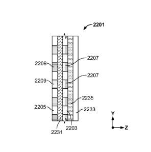
are left in an
untreated state, the light sheet emits light from both edges. The laser etch
mark 1511 can
enhance the light output on only one edge (in this illustration, the left hand
side) and
decreases the light output on the opposite edge (in this illustration, the
right hand side) by
reflecting the photons back into the edge lighting device. The laser etch mark
1511 can also
output photons so that the laser etch mark 1511 has an illuminated appearance.
[00165] In one variation, the second edge 1515 can be formed as an existing
mechanical
cut which emits light, which is formed when the sheet of light sheet is
mechanically cut to be
separated into individual light sheet strips.
[00166] In addition to, or as an alternative to, the laser etch mark 1511,
one edge can be
treated (cut) to allow the light to pass through; the other edge is treated to
redirect the light
back into the product.
[00167] Method of Surface Treatment to Enhance Light Properties
[00168] Referring now to FIG. 16A to 16D, cross sectional views of a method to
produce
an edge lighting device will be discussed and described. In connection with
FIG. 16A to
16D, articles and processing methods used to produce various properties will
now be
discussed relating to applying a film layer on top of the edge lighting device
to couple
additional light generated by the LED to the second edge, which is the part of
the lighting
device that is illuminated.
[00169] The edge lighting, such as for a door panel, in this example can
include the
following properties. Examples of color can include white, blue, green, red,
and/or amber.
CA 02840244 2013-12-20
WO 2013/016646
PCT/US2012/048569
For blue, a blue ILED can be used, in some embodiments with a 1/4" spacer, die
height of 4
mil (0.004 inches), a 3 mil hot melt adhesive, 5 mil PET for bottom and top
substrates, optic
film and/or a hi reflective metalized film like chrome. An optic film can be,
e.g., i/4" in width
and 6" in length.
[00170] The outline in FIG. 11B can be further illustrated in FIG. 16A,
processing steps
for preparing an optic film 1601 (an example of which is a translucent
diffusion film) as
discussed herein before adding to the lighting device can include (1)
providing the optic film
in raw form, (2) folding the film length wise in half, and (3) using a
laminator to obtain a
good crease across the center.
[00171] Then, as illustrated in FIG. 16B, (1) a light sheet is prepared to
be manufactured
for use in the edge lighting device. For example, the light sheet before
manufacture is formed
in a strip to include a single linear strip of LEDs, spaced apart, for
example, 40 LEDs
provided on a 10" x 0.5" strip. The light sheet prior to manufacture can
include bottom
substrate 1605 with LEDs embedded therein and a bus tape 1603, and a top
substrate 1609
with a bus tape 1607. (2) Then, the top and bottom substrates are laminated
together in
accordance with known techniques to form a light sheet 1613 with buses 1611
that can be
powered on.
[00172] Referring now to FIG. 16C, the prepared optic film is placed along a
front edge of
the manufactured light sheet, with the creased area adjacent to the buses 1611
edge of the
manufactured light sheet 1613, with a flap area of the prepared optic film
1615 each on the
top and bottom of the manufactured light sheet.
[00173] As shown in FIG. 16D, a metalized chrome tape 1617 is then placed on
the top
and bottom of the light strip. Photons generated by the LEDs in the
manufactured light sheet
1613 are reflected off the metalized chrome tape 1617 (which is representative
of a metalized
film), back into the light sheet 1613, to eventually be directed towards the
second edge of the
edge lighting device from which the photons are allowed to be emitted.
[00174] Such a method as outlined herein can yield a product suited for
applications where
concealed lighting is required or desired.
[00175] Metalized Treatment
[00176] FIG. 26 illustrates a cross section of an edge lighting device 2601,
suitable, for
example, for use in a concealed lighting application. Referring now to FIG.
26, a cross
sectional view of a concealed lighting example will be discussed and
described. Layer A,
21
CA 02840244 2013-12-20
WO 2013/016646
PCT/US2012/048569
layer B, and layer C 2603, 2605, 2607 are sandwiched in this order, and
collectively comprise
an edge lighting device 2601. Layer A 2603 can be a translucent material such
as ink or a
metalized film such as chrome that can be applied to a top of Layer C 2607.
Layer C is an
edge lighting device or uniform lighting device as further discussed herein.
Layer A and
Layer C 2603, 2607 sandwich Layer B 2605. Layer B is an adhesive film which
adheres the
metalized film 2603 to Layer C 2607.
[00177] As a daytime mode of operation, the light sheet assembly layer C in
the lighting
device can be un-powered. In the daytime mode, the edge lighting device or
uniform lighting
device with a metalized film of FIG. 16D has a chrome appearance, with the
light concealed
by the translucent material. As a night time mode of operation, the light
sheet assembly in
the lighting device can be powered for a dramatic illuminated appearance. In
the night time
mode, the uniform lighting device has a lit appearance per the light sheet die
pattern. As an
example, refer to the FLEX logo 3105, 3135 illustrated in FIG. 31A and FIG.
31B for a day
and night time picture of a concealed light with pre-patterned LEDs in the
light sheet.
[00178] Color Variations
[00179] Referring now to FIG. 17, illustrations of properties of edge lighting
will be
discussed and described. Using techniques known to one trained in the art,
more than one
color of LED can be included where select LEDs in different discrete colors or
different color
LEDs in combination, can create unique colors. This illustration shows an
upper lighting
device 1701 and a lower lighting device 1721. In the upper lighting device
1701, there is
provided a color mixing amber (A) on a top trace 1703 and a red (R) on a
bottom trace 1705.
Power can be provided to the lighting device 1701 via power lines 1711, 1709,
1707. When
powered, the amber and red colors mix to create orange light output from the
lighting device.
The lighting device 1701 of this embodiment can have a top substrate width >
1.0".
[00180] In the lower lighting device 1721, there is provided a color mixing
amber (A) on a
top trace 1723 and a red (R) on a bottom trace 1725. Power can be provided to
the lighting
device 1721 via power lines 1731, 1729, 1727. When the top trace and bottom
trace 1723,
1725 are powered simultaneously, the amber and red colors mix to create orange
light output
from the lighting device.
[00181] Also, the upper and lower lighting devices 1701, 1721 show the impact
which die
spacing has on the uniformity and mixing. Hot spots can be reduced when the
die are spaced
closer together than when the die are spaced further apart.
22
CA 02840244 2013-12-20
WO 2013/016646
PCT/US2012/048569
[00182] Fabric Embodiment
[00183] Sewing through the lighting device allows for easy attachment to
fabric and will
not interrupt performance for edge or back lighting. Penetrating the upper and
lower layers
of the lighting device does not break circuit connections allowing the full
function to
continue. Also, because of the adhesive used between these two layers, when a
puncture
occurs, the sealant maintains adhesion and keeps the lighting device
environmentally sealed.
[00184] Reference is now made to FIG. 17, illustrating that a lighting device
1751 can be
sewn on to fabric 1753. The fabric 1753 can be a conventional material. The
lighting device
1751 can be stitched to or woven into the fabric using known techniques for
attaching fabric,
for example, stitching or gluing along a seam, as edging, as decorative
treatment, and the like.
The die portion of the lighting device 1751 can be positioned away from the
stitches so that
the LED is not punctured. The lighting device can be very robust to
stress/twisting/bending
where the fabric is sewn. Potential applications include: seats, headliners,
and various
clothing type products.
[00185] Further discussion is provided herein with regard to various
embodiments
involving fabric.
[00186] Comparative Example ¨ Metalized Film
[00187] Reference is now made to FIG. 18A and 18B.
[00188] Light sheet strips were built on PolyCu, with 0.5" ILED spacing, and
top substrate
with widths of 1" and 1.5" evaluated for light emitted to the edge. FIG. 18A
illustrates
samples of the raw product. In FIG. 18A, an edge lighting device 1851 is
illustrated from a
top-view. The edge lighting device can include a first portion 1853 which is
covered by a
translucent metalized film, and a second portion 1855 which is covered by a
translucent
diffusion film. The edge lighting device 1851 can be prepared as discussed in
connection
with FIG. 11B, for example.
[00189] Referring now to FIG. 18B, a comparative illustration of cross
sections of edge
lighting devices of different widths will be discussed and described. FIG. 18B
illustrates
putting the chrome film on top and bottom of a wide lighting device and a
narrow lighting
device. The chrome film 1803, 1825 increases the intensity of the light which
is output from
the lighting devices. The chrome film 1803 on the wide lighting device has a
width 1809 of
1.5 inches. The chrome film 1825 on the narrow lighting device has a width
1829 of 1 inch.
In these examples, part of the light sheet 1801, 1821 is covered with the film
and at least one
23
CA 02840244 2013-12-20
WO 2013/016646
PCT/US2012/048569
edge is not covered. This comparison illustrates that the chrome film 1803,
1825 increases
the light intensity, and that the width of the chrome film changes the
appearance of the light
output from the edge lighting devices. It was observed that the wide lighting
device with the
wide chrome film 1803, 1805 having a width 1809 of 1.5" provides a more
uniform light,
whereas in comparison the narrow lighting device with the chrome film 1825
having a width
of 1" is more intense but less uniform. In the edge lighting devices, the
chrome film 1203,
1825 is folded over a light sheet strip 1801, 1821 to sandwich the chrome film
1803, 1825.
In these examples, the light sheet strip 1801, 1821 abuts a fold in the chrome
film 1803,
1825. The chrome film 1803, 1825 can be attached to light sheet strips 1801,
1821 utilizing,
for example, an adhesive tape (not illustrated). Opposite sides of the chrome
film 1803, 1825
which face each other can be adhered using an adhesive 1807, 1829. The
adhesive 1807,
1809 can be translucent or transparent.
[00190] The wide and narrow edge lighting devices were evaluated and compared
using
chrome film 1803, 1825 folded over on top and bottom substrates of the light
sheet 1801,
1821. The highly reflective chrome film will increase the intensity of light
seen at the edge
of the edge lighting device. See FIG. 18B. The LED light source (within the
light sheet) was
more noticeable as a point light source in the narrow lighting device than in
the wide lighting
device. . The edge lighting device with the chrome film was compared to a
lighting device
without the chrome film; a uniform light was achieved on the edge of the
lighting device
without the chrome film on top and bottom substrates.
[00191] Spacer Variation and/or Angle to Control Intensity and Width
[00192] Reference is now made to FIG. 19A and FIG. 19B, in order to explain
another
method for creating an edge light using a flat edge lighting device 1951. FIG.
19A is a cross
section, and FIG. 19B is a top view thereof. This variation is similar to the
previously
discussed edge lighting device illustrated for example in connection with FIG.
11B, and
discussion of similar portions is omitted. In the present embodiment, however,
a spacer can
be utilized to control a top-to-bottom depth of the edge lighting (when
viewed, how thick or
narrow the edge lighting appears) and/or a diffusion/intensity of the light
emitted from the
edge lighting device. Some elements which arc discussed elsewhere herein are
omitted from
the present discussion. Without the spacer, an edge lighting device can
provide a very
narrow ribbon of light; the spacer can be used to increase the apparent
thickness of the ribbon
of light.
24
CA 02840244 2013-12-20
WO 2013/016646
PCT/US2012/048569
[00193] Referring to FIG. 19A, a cross section view of an edge lighting device
will be
discussed and described. An edge lighting device 1901 can include an
enhancement film
1903, plural LEDs (here represented by LED 1905), a first conductive trace
1907, a spacer
1909, a top diffusion film 1911, a top electronically conductive substrate
1913, an adhesive
1915 into which the LED 1905 is embedded, and second conductive traces 1917.
The spacer
1909 can provide a uniform intensity and a thicker edge light in comparison to
a lighting
device without a spacer. The spacer 1909 can be formed of an acrylic film. If
the acrylic
film, as well as other layers in the edge lighting device 1901, is flexible,
the edge lighting
device has a flexible property. By using an acrylic film spacer between a
light sheet and the
enhancement film, a thicker edge light is provided. An example use of the
device of FIG.
19A is illustrated in FIG. 5 and FIG. 6, in which the desired width of the
edge lighting device
has been achieved by use of a spacer to expand a width of the edge light.
O01-94 n a variation, the light output can be at an angle so that the edge
lighting device
does not have to be on edge. That is, the edge may be cut at an angle other
than at a right
angle to the top or bottom of the transparent surface to increase width of the
"ribbon of light".
[00195] Referring now to FIG. 19B, a top view of the edge lighting device will
be
discussed and described. The edge light which is produced from the edge
lighting device
1951 can be thin, for example, less than 0.025 in width. Furthermore, the
light which is
produced from the edge lighting device 1951 can have a uniform light around
the corners,
because the light is produced from the LEDs which are uniformly spaced apart
from a nearest
portion of the surface of the front edge (i.e. the edge which is illuminated),
regardless of the
bending of the edge lighting device. The edge lighting device 1951 can be
formed of flexible
or semi-flexible materials if desired, instead of being formed of rigid. The
thickness of
appearance of different edge lighting devices can be varied as desired, based
on focal length,
die pattern, and enhancement film used.
[00196] Lighting Applications
[00197] The lighting devices discussed herein can be used in connection with
various
applications. The principles of the lighting devices for various lighting
applications can be
ascertained with reference to the following examples of applications in which
the edge
lighting technology or the uniform lighting device using the light sheet can
be used: Car Door
(FIG. 1, FIG. 2), Console (FIG. 3), Cup Holder Edge Lighting (FIG. 4), and
charge ring with
CA 02840244 2013-12-20
WO 2013/016646
PCT/US2012/048569
edge light (FIG. 5, FIG. 6). FIG. 1 was discussed in more detail above. FIG. 2
to FIG. 6 are
now discussed in more detail below.
[00198] Referring now to FIG. 2, a view of an edge lighting device in a
vehicle door will
be discussed and described. FIG. 2 illustrates an edge lighting device with
some sharp
comers. Here, the edge lighting device has a generally polygonal shape, in
which rounded
corners 23, 25, 29, 31 are spaced apart by straight portions 21, 27, 30, 37.
Here, two of the
comers 23, 31 are generally at an acute angle, and two other comers 25, 29 are
generally at
an obtuse angle. The illumination of the edge lighting device is distributed
evenly throughout
the light edge. The edge lighting device is disposed to be sandwiched in a gap
which is
normally formed between two or more pre-formed pieces of automotive molding
39, 41 in a
car door.
[00199] In FIG. 2, color is indicated by hatching in element 41.
[00200] Referring now to FIG. 3, a view of an edge lighting device in
connection with a
console will be discussed and described. A console 301 for use in an
automotive device is
arranged to include edge lighting devices sandwiched within various gaps
molded into the
console 301. In this example, the edge lighting devices include first and
second edge lighting
devices 303, 309 disposed in an interior of cup holders in the console 301; a
console base
edge lighting device 305 disposed along an edge at the base of the console
301, at a
preformed gap between the console 301 and a base 307 on which the console
sits.
[00201] A lighting device 311 can also be positioned at a corner of the
console 301 to
provide additional lighting within the automobile.
[00202] In FIG. 3, color is indicated by hatching in element 403.
[00203] Referring now to FIG. 4, a view of an edge lighting device in
connection with a
cup holder will be discussed and described. A first edge lighting device 403
is disposed in
the gap between a pre-formed cup holder insert 405 and a body of a cup holder
401.
Optionally, a second edge lighting device 407 can be disposed in a gap formed
between the
cup holder insert 405 and bottom of the cup holder insert.
[00204] FIG. 5 and 6 are an example of a stacked edge lighting, in which edge
lighting of
different colors is stacked to achieve different selectable colors. FIG. 5
illustrates a device
with a single discrete light sheet formed from stacked light sheets which each
have a different
color from each other, and FIG. 6 illustrate the selective lighting of one
sheet of the stacked
sheets in the lighting device.
26
CA 02840244 2013-12-20
WO 2013/016646
PCT/US2012/048569
[00205] Referring now to FIG. 5, a view of an edge lighting device in
connection with a
charge ring will be discussed and described. A composite lighting device 501
comprises a
lighting body 503 and an edge lighting device 505 disposed within a gap formed
in the
lighting body 503 and positioned so that the edge light is displayed to a
user. In this
composite lighting device 501, the edge lighting device 505 comprises plural
light sheets.
Each of the light sheets within the edge lighting device 505 includes LEDs of
respective
different colors. In this example, the four light sheets are stacked, one with
white LEDs, one
with yellow LEDs, one with red LEDs and one with green LED. White is obtained
by using
high energy blue LEDs behind a yellow phosphor overlay. The energy of the blue
LEDs
excite the phosphor producing photons and the color combination of blue &
yellow phosphor
produces the white light. The edge lighting can be stacked to achieve
selectable different
colors. Alternatively, a discrete light sheet of a combination of colors,
e.g., yellow and red,
can be put together. FIG. 5 illustrates a selection device 507 which provides
individually
selectable power on/off to each of the light sheets in the edge lighting
device 503. The
selection device 507 can include a selection control 511 for each respective
color 513, 515,
517, 519 or power all on 521. It should be noted in this embodiment that the
composite
lighting device 501 is configured as a charge port.
[00206] Referring now to FIG. 6, another view of an edge lighting device in
connection
with a charge ring will be discussed and described. In FIG. 6, the same
composite lighting
device 501 is shown with each different light sheet separately illuminated. By
selectively
powering on or off a light sheet with color LEDs, an edge lighting device can
be switched
between modes in which it appears as a red color edge lighting device 601, a
green color edge
lighting device 603, a white color edge lighting device 605, and a yellow
color edge lighting
device 607. The color is indicated by hatching in the respective designs. The
composite
lighting device 501 can be powered off, in which case there is no
illumination.
[00207] Features and Benefits
[00208] Although features and possible benefits have been discussed elsewhere
in this
document, the following can be noted.
[00209] Thickness: the edge lighting device can have an overall thickness from
top to
bottom which can be less than 0.02", which enables the emitted light to be of
comparable
thickness. The edge lighting device can be installed into spaces/gaps that
were designed to
account for tolerances in the mounting product.
27
CA 02840244 2013-12-20
WO 2013/016646
PCT/US2012/048569
[00210] Flexible: a sample edge lighting device was mounted as a straight or
curved
styling feature at radiuses at least down to 1".
[00211] Light weight: a sample size of 10" X 0.5" X 0.025" was created with a
weight of
<10 grams
[00212] Customized Single and Multi-color: An edge lighting device can have
stacked
light sheets to create individually controlled lighting or on the same
substrate to enable color
mixing.
[00213] Uniform lighting: Even lighting with a uniform and homogenous
appearance on
the lit surface around corners and straight edges was achieved
[00214] System Flexible design:
DC Voltage Drive
No EMI concerns
Dimmable with simple constant current or analog control
No ballast or high frequency waveform required
No TR or UV radiation for products emitting light in the visible spectrum
[00215] Reliability:
No wire bond. Wire bond can lead to electrical over stress (EOS) type failure
modes in packaged ILEDs
No organic material degradation concerns as seen with OLEDs
Can be sealed from water penetration or from exterior environment via potting
or
overlays.
One solid part with no moving parts ¨ eliminate squeak and rattle issues
[00216] Opaque/Transparency Variation ¨ Finding 14 1
[00217] The edge lighting device or uniform lighting device can be transparent
on one of
the top and bottoms sides, and the other of the top and bottoms sides can be
opaque or
transparent. An example of a product that is opaque when un-powered is a
Center High
Mount Stop Lamp (CHMSL).
[00218] The light sheet device/method used to make it can have at least one
optically
transparent electrically conductive film, as used herein.
[00219] Ambient Condition Variation - Finding #2
28
CA 02840244 2013-12-20
WO 2013/016646
PCT/US2012/048569
[00220] The device/method can provide an ability to have a smart light based
on ambient
conditions. This can be realized by selecting different pattern die or
reducing the intensity.
FIG. 20A shows some features of a smart light.
[00221] Referring now to FIG. 20A, features of a smart light will be discussed
and
described. A light is an example of a device, based on a light sheet, which
can be provided
with an ambient sensor such as one in which resistance changes with incident
light. Incident
light i can provide a current that varies with resistance and change due to
the ambient light
condition. The variation in incident light directly relates to the lumens or
candela output
from a light sheet product 2003 in this embodiment. A light sheet product 2003
formed of a
light sheet can receive a DC voltage 2007 via a variable resistor 2005 that
changes resistance
according to incident light, in accordance with known techniques. The output
current 2001
varies according to the incident light.
[00222] Homogeneous/Uniform Lighting Device ¨ Finding # 3
[00223] A method and device for creating a homogenous/uniform light source,
including
uniformity of light around corners, is now discussed in particular. A
homogeneous/uniform
lighting device is sometimes referred to herein as a "homogeneous light
source" or
"homogeneous lighting device" or "uniform lighting device" or
"homogenous/uniform
lighting device". The homogeneous appearance is a major, desired appearance
goal of many
lighting product customers and is often difficult to achieve in LED lighting
luminaires.
[00224] Referring now to FIG. 20B a cross section of a homogeneous light
source will be
discussed and described. A homogenous light source 2051 can include a light
enhancing or
diffusing film 2053, a spacer or air gap 2055, a transparent electrically
conductive top
substrate 2061, a plurality of LEDs 2063 embedded in an adhesive layer 2057,
and an
electrically conductive bottom substrate 2059. Multiple light rays such as
2065a are emitted
from each of the LEDs 2063 and travel through spacer or air gap 2055 and will
be controlled
by the light enhancing or diffusing film. The spacer or air gap 2055 provides
the "focal
length" to enable the light enhancing films to function. Some of the light
rays emitted from
the LED are diffused into the transparent electrically conductive top
substrate 2061 and are
directed to the first and second edges of the top substrate 2061 as discussed
previously.
[00225] A homogeneous light can be created with a die pitch as measured from
center to
center of adjacent LEDs 2063 is > 2 x spacer width A between the light
enhancing or
scattering diffusing film 2053 and the transparent electrically conductive top
substrate 2061.
29
CA 02840244 2013-12-20
WO 2013/016646
PCT/US2012/048569
[00226] The intensity of the light can be adjusted manually or automatically.
This
illustration shows how a homogeneous light can be created from a device based
on a light
sheet.
[00227] An example of a homogenous lighting device, and one method to create a
homogenous/uniform light is illustrated in FIG. 21A, FIG. 21B, and FIG. 21C.
These figures
will now be discussed. Referring to FIG. 21A, the cross section shows, in
order from the top
down, (1) a lens (optional) such as an acrylic or polycarbonate lens 2115, (2)
a first adhesive
layer, such as a tape or adhesive 2103, (3) a light diffusing and / or
enhancing film 2105, (4) a
second adhesive layer, such as a tape or adhesive 2107, (5) a transparent
spacer (such as an
acrylic spacer 2109 or an airgap, adjusted to a pre-determined focal length,
(6) a third
adhesive layer, such as a tape or adhesive 2111, and (7) a light sheet layer
2113. Here, LEDs
in combination with the materials depicted in FIG. 21A are used to create a
uniform light
with a very thin thickness. The "light sheet layer" can be made according to
known
techniques, for example, as disclosed in US 2008/0079012, and variations
thereof, as the so-
called "light sheet layer". The combination of these thicknesses and the type
of diffusing and
/or /enhancing film and the focal length provides a homogenous look, as
illustrated for
example in FIG. 20B. Other methods using different combinations and material
thicknesses
can be used to create a homogenous/uniform light as well. For instance
additional layers of
diffusing/enhancing films in combination with different spacer thicknesses.
Furthermore,
light that leaks out the sides of the clear spacer can be absorbed or re-
directed back into the
lighting device by using opaque or highly reflective material respectively.
[00228] Hatching is used to indicate colors in FIG. 21A-21C, for the stop-tail
lamp, turn
signal and back up lamp.
[00229] Reference is now made to FIG. 21B, a rear view of a tail lamp and FIG.
21C, a
rear view of another tail lamp, in which the cross-section material of FIG.
21A is used. The
phrase "rear view" refers to the view from a rear toward the front of an
automobile in which
the tail lamp may be installed. The acrylic (or other clear plastic material)
spacer relates to a
focal length. The depth of the spacer can be determined using known techniques
to achieve
the desired focal length. By adding the layers onto the light sheet, a
particular visual effect
can be obtained. The focal length can improve performance and appearance. If
the film was
directly applied to the conventional light sheet it would not be homogenous,
in comparison to
adding the spacer to achieve the focal length necessary for a
homogenous/uniform light.
CA 02840244 2013-12-20
WO 2013/016646
PCT/US2012/048569
[00230] Referring now to FIG. 21B, a rear view of a lamp in which the cross-
section
material of FIG. 21A is used will be discussed and described. FIG. 21B is an
example of an
integrated lamp 2131, such as an integrated stop - tail, turn (red or amber)
or back up.
Amber, red, and white ILEDs were distributed in pre-formed first, second, and
third different
color sections 2133, 2135, 2139, and were die bonded onto the same bottom
substrate to
create the light sheet, for example, to meet FMVSS or other countries'
equivalent regulatory
requirements. The manufacture of the light sheet with the pre-formed first,
second and third
different color sections can be completed according to known techniques. An
acrylic spacer,
lens, and the like as discussed in connection with, e.g., FIG. 21A can be
layered onto the light
sheet with the pre-formed first, second and third different color sections to
form a single
unitary light in which all layers are edge-to-edge unitary substrates. This
can yield a uniform
tail lamp with a thickness down to ¨ 5mm or 0.2". The cross section (see FIG.
21A) can be
applicable for all uniform light sheet products as disclosed herein.
[00231] In FIG. 21B, red, amber and white LEDs were used in conjunction with
spacers
and light enhancing film.
[00232] Referring now to FIG. 21C, a rear view of another lamp in which the
cross-section
material of FIG. 21A is used will be discussed and described. FIG. 21C is a
rear view of a
tail lamp 2151 in which a uniform light is achieved around the corners. The
uniform light
can have a width that can vary based on the die pattern and enhancement film
used. In
operation, photons emitted from the die embedded in the light sheet substrate
material emit
light in a Lambertian pattern obtaining a half angle at +60 . When the photons
reach the
surface of the enhancement film, which has a +40 spread in both the
horizontal and vertical
axis, maximum performance for light output is achieved at a predetermined
focal length and
die pattern. In this example, the light sheet was manufactured with a pre-
formed pattern of
LEDs in first and second different colors 2153, 2155.
[00233] Referring now to FIG. 20C, a uniform light around corners will be
discussed and
described. FIG. 20C illustrates that a uniform light can be realized around
corners, which is
not achievable using light pipe type technology. As shown, in the homogenous
lighting
device 2071 discussed herein (on the left side of the figure), there is a
uniform light,
including around the corner 2073 which has a same lighting distribution and
intensity as in
perpendicularly arranged legs 2075, 2077. In comparison, using conventional
light pipe
device 2081 (illustrated on the right of FIG. 20C), the light is not uniform
and is not evenly
31
CA 02840244 2013-12-20
WO 2013/016646
PCT/US2012/048569
distributed at a corner 2083 in comparison to non-corner portions such as legs
2085 and 2087
which are perpendicularly arranged.
[00234] To illustrate what is meant by a "uniform light" or "homogenous
light", reference
can be made to the following figures, which are photographs of example
homogenous
lighting devices:
FIG. 41A, showing a Double Row CHMSL Full Mold MG unpowered
(homogenous lighting device in white)
FIG. 41B, showing a Double Row CHMSL powered daytime (homogenous
lighting device in red)
FIG. 41C, showing a Double Row CHMSL Full Mold MG 2084 powered
nighttime (homogenous lighting device in red), and
FIG. 41D, showing a Row Dome MG 3071 powered daytime (homogenous
lighting device in white).
FIG. 41E, showing a mounted Signal Lamp, powered.
[00235] The photographs of the powered lighting devices illustrate the
homogenous light,
which is uniform throughout the light, from end-to-end, along both the
horizontal and the
vertical directions, as well as out to the corners.
[00236] As mentioned above, FIG. 20C illustrates light around corners. On the
left figure,
the uniform lighting device 2071 achieves uniform light around corners, in
which the
intensity and diffusion of the light at the corner and legs 2073, 2075, 2077
is the same. In
comparison, the figure on the right is a conventional lighting device and the
light at the
corner 2083 of the conventional device 2081 is diminished in comparison to the
legs 2085,
2087.
[00237] In conventional lights, a conventional air gap plus optics in the lens
can be used to
control the light. The light passes through the air gap, and then through a
lens; the back side
of the lens has optics that help direct the light. The present embodiment does
not need to use
the optics in the lens. For example, referring back to the cross section of
FIG. 21A, the
acrylic or polycarbonate or other lens does not need to use any additional
optics to control the
light. Thus, the homogenous lighting device does not need special molds for
preparation of
the lens. Also, it can be light weight, flexible, and can get to market
quickly since no special
molds are required.
[00238] Finding #4 ¨Integrated Rear Combination Lamp, Light Sheet Lighting
System
32
CA 02840244 2013-12-20
WO 2013/016646
PCT/US2012/048569
[00239] Reference is made back to FIG. 21B. A conventional tail lamp has
multiple
different parts. In the illustrated embodiment, all of the features with the
different colors (tail
lamp, turn signal, back-up) and uncolored parts 2133, 2135, 2139, 2137 can be
a single
unitary part, still maintain thickness in, e.g., 0.2 inch range, and still be
individually
controlled with electronic circuitry/feature external to or integrated on the
single unitary part.
The integrated combination lighting device can be provided as a very thin
light and provide
multiple functions (colors) using the same substrate. This can be a big
advantage for
situations where one lamp can provide multiple functions.
[00240] Integrated Flexible Circuit Variation
[00241] The control part can be a flex circuit such as illustrated in FIG. 27,
an electrical
schematic in block diagram form of a light sheet assembly.
[00242] Referring now to FIG. 27, a schematic of a flex circuit will be
discussed and
described. A flex circuit 2700 can include a light sheet product 2701
receiving a signal from
control circuitry 2703. Input to the control circuitry 2703 are a voltage
regulation signal 2705
and a signal from a control module 2713, such as a standard in-vehicle control
computer.
The voltage regulation signal 2705 receives a signal from a latch 2707, which
receives a
latched signal 2709, which receives an inserted signal 27011 originated from a
multi-voltage
input source 2715.
[00243] The electronic circuitry for a courtesy light and a CHMSL
respectively, such as
illustrated in FIG. 27, can be incorporated for the following
reasons/functions:
(1) Input voltage reduction
(2) Protection from vehicle transients
(3) Noise reduction / de-bounce from power switches
(4) Power switches like membrane type
(5) Control for addressing intensity "light", and color mixing.
[00244] All of the above functionalities (1)-(5) plus the light sheet can be
assembled onto
the same flexible circuit. The additional electronic circuitry can be placed
using the same
equipment for placing the LED die used in the light sheet product. Placement
can include the
conductive epoxy to mechanically and electrically attach the component to the
flexible circuit
and the actual electronic parts.
[00245] Referring now to FIG. 28, an illustration of an integrated electronic
circuit will be
discussed and described. FIG. 28 illustrates an example of how the electronic
circuitry can
33
CA 02840244 2013-12-20
WO 2013/016646
PCT/US2012/048569
be integrated on to the same flexible circuit containing the light sheet. In
FIG. 28, element A
2803 is a membrane switch, element B 2805 is an electrical circuit (e.g.,
protection, noise
control and control circuit) and element C 2807 is a light sheet circuit. The
membrane switch
2803 can be a conventional membrane switch. The electrical circuitry 2805 can
be as
disclosed in FIG. 27, or variations thereof. The light sheet circuit can be as
disclosed in
connection with FIG. 11B, FIG. 20B or FIG. 21A herein. The membrane switch
2803
generates a control signal to the electrical circuitry 2805, which is
electrically connected to
and controls the light sheet circuit 2807.
[00246] Referring now to FIG. 29, an illustration of an over-mold will be
discussed and
described. A lighting device 2901, for example as illustrated in FIG. 27 or
FIG. 28, can be
further enhanced by either over-molding or laminating a decorative cover, as
illustrated in
FIG. 29. In FIG. 29, elements A are over-molds 2903, 2907 and element B is a
light sheet
circuit area 2905.
[00247] The light sheet circuit area can be a single part, as discussed above.
Optionally,
the light sheet circuit area can include different colors on the same
substrate.
[00248] Integrated Combination Light Variation
[00249] Reference is made to FIG. 22A and FIG. 22B, which illustrate a CHMSL
and
map/courtesy light on two different surfaces of the same substrate 2201. FIG.
22A is the top
view of surface "A" and surface "B", and FIG. 22B is the side view of the
combination
CHMSL and map/courtesy light. Surface "A" is a CHMSL light source, and surface
"B" is a
map or courtesy light source. The CHMSL will be directed to the exterior of
the vehicle, and
the other surface will be directed to the interior of the vehicle. Surface "A"
and surface "B"
are on opposite surfaces of the same substrate 2201. Hatching is used to
indicate colors in
FIG. 22A-22B.
[00250] Referring now to FIG. 22A, a top/bottom view of light on two different
surfaces
of the same substrate will be discussed and described. An integrated
combination light is a
combination of layered substrates 2201 and includes surface "A" 2203 and
surface "B" 2205,
on an opposite side of the same layered substrates 2201. Surface "A" 2203 can
include point
light sources 2207 or optionally can be provided as a homogenous light source
2223. Surface
"B" 2205 can include point light sources 2209 or optionally can be provided as
a
homogenous light source 2225. The homogenous light source can be provided as a
homogenous lighting device, discussed above. The point light source can be
provided as a
34
CA 02840244 2013-12-20
WO 2013/016646
PCT/US2012/048569
non-homogenous light source such as a light sheet. Surface "A" and surface "B"
can be
provided in different colors, for example, the colors appropriate to a CHMSL
in surface "A"
2203 and colors appropriate for a map or courtesy light in surface "B".
Surface "A" 2203
and surface "B" 2205 can be combined into the same substrate as shown in cross
section,
FIG. 22B.
[00251] Referring now to FIG. 22B, a side view of a light on two different
surfaces of a
same substrate will be discussed and described. In FIG. 22B, an integrated
combination
lighting device of layered substrates, 2201 includes a first substrate 2205,
e.g., a courtesy
light, a second substrate 2231 which is the common conductive substrate or
separate
substrates adhered with, e.g., tape, and a third substrate 2203 is, e.g., a
CHMSL. Also
illustrated is a fourth substrate 2235 is adhesive such as tape, and a fifth
substrate 2233, for
example an automobile's back window on which the integrated light sheet
lighting device can
be adhered. The first substrate 2205 incorporates LEDs 2209 in all appropriate
color(s) and
arrangements for the first light display 7 e.g., a courtesy light; and the
second substrate 2203
incorporates LEDs 2207 in an appropriate color and arrangement for a second
light display,
e.g., a CHMSL.
[00252] Finding #5 ¨ Integrated Dual Light Sheet Lighting System
[00253] An integrated dual lighting system can be provided, such as a tail
lamp feature
with an additional lighting feature. Still referring to FIG. 22A and FIG. 22B,
other examples
are a reading/map light, for example in white made with stacked light sheet
that is laminated
or uses a common bottom substrate for an interior application, and a regulated
light property
on the opposite side to provide a CHMSL function for an exterior application.
Other
examples are a CHMSL/Cargo light on the same substrate, and a stop/tail/turn
light on the
same substrate.
[00254] The features can be integrated on the same plane of the same
substrate, and/or
integrated on opposite sides of the same substrate combination. For example, a
first surface
can have the CHMSL feature (facing outside), and a second of the same
substrate (facing
inside) can have a reading light or map light shining into the interior of the
vehicle.
[00255] The integrated combination lighting device can be provided as a very
thin light.
[00256] Glass Laminated Variation
[00257] According to another variation, the CHMSL can be laminated in glass.
Referring
now to FIG. 46, a multi-strip laminated in glass will be discussed and
described. A CHMSL
CA 02840244 2013-12-20
WO 2013/016646
PCT/US2012/048569
4605 can be prepared as discussed above. The CHMSL 4605 can be sufficiently
thin so as to
be laminated to glass 4601, for example in accordance with known techniques.
The CHMSL
4605 can be powered by an electrical connection 4603 to a conveyance.
[00258] Finding #6 ¨ Exterior Architectural Applications
[00259] Referring now to FIG. 23, an illustration of exterior lighting
applications will be
discussed and described. FIG. 23 provides non-exhaustive examples of exterior
lighting
applications in connection with a conveyance 2301, for the edge lighting
device and/or the
homogenous lighting device discussed herein. An embodiment can provide for
architectural
lighting in the exterior of a conveyance system. Lighting can be independent
or integrated
with another light sheet lighting device or a conventional non-light sheet
lighting system.
Hatching is used to indicate colors in FIG. 23.
[00260] Examples of lighting include an underbody strip light 2305 or step-up
rail, a kick
plate 2307, a perimeter light around a wheel well 2309, window treatment light
around a
window 2303, a light source on a mirror 2315, a perimeter light around a grill
2313, and a
light in a headlamp 2311.
[00261] For example, a, edge light in a white color can be integrated into a
front headlamp,
as further shown in FIG. 36.
[00262] Misc. Interior and Exterior Applications
[00263] FIG. 30A-30F, FIG. 31A-31B, FIG. 32A-32B, and FIG. 33-FIG. 36 have
several
examples of light sheet Interior/Exterior Applications, which are presented by
way of
example and not limitation. It will be appreciated that one, or all, or a
combination of the
example interior and exterior applications can be provided. Not all of these
examples need to
be provided. Hatching is used in these figures to indicate colors which are
generated by the
LEDs when the LEDs are powered on.
[00264] Referring now to FIG. 30A to FIG. 30F, examples of interior and
exterior
applications will be discussed and described. In FIG. 30A, interior switches
are backlit with
an edge lighting device 3001. In FIG. 30B, a door handle is provided with an
edge lighting
device 3011. In FIG. 30C, a perimeter of a window is provided with an edge
lighting device
3021. In FIG. 30D, a hitch 3033 is provided with marker lights 3031. In FIG.
30E, a
perimeter of a grill 3041 and a perimeter of a headlamp 3043 are provided with
an edge
lighting device. In FIG. 30F, a car window 3051 is provided with a homogenous
lighting
device 3053 as a CHMSL.
36
CA 02840244 2013-12-20
WO 2013/016646
PCT/US2012/048569
[00265] Referring now to FIG. 31A and FIG. 31B, an interior application for a
door panel
at night time and day time, respectively will be discussed and described. In
the nighttime
view of FIG. 31A when the lighting devices arc illuminated, the lighting
devices are visible.
In comparison, in the daytime view of FIG. 31B, the lighting devices are not
visible.
[00266] FIG. 31A illustrates a door panel 3101 for an automobile that includes
a
homogenous lighting device as an interior light 3103, as a decorative panel
3105, and as a
speaker cover 3109; and an edge lighting device as an arm rest trim strip
3113, a door pocket
light 3107, and a door pocket decorative insert 3111.
[00267] FIG. 31B illustrates a door panel 3131, which is the same door panel
shown
during daytime. The door panel 3131 illustrates an interior light powered off
3133, a speaker
cover 3139, powered-off door pocket light 3137, powered-off decorative insert
3141,
powered-off arm rest trim strip 3143, and powered-off decorative panel. During
the daytime
and/or when the edge lighting devices and homogenous lighting devices are
powered off, the
edge and homogenous lighting devices are not noticeable and may not be
distinguishable
from the trim panels into which they are inset.
[00268] Referring now to FIG. 32A, an interior application under seat will be
discussed
and described. Here, a homogenous or edge lighting device (not visible) is
placed on the
bottom of a seat 3201 to illuminate a floor area 3203 under the seat 3201.
[00269] Referring now to FIG. 32B, an interior application in a cup holder
will be
discussed and described. Here, an edge lighting device 3215 is placed inside a
cup holder,
and an edge lighting device 3213 is placed as trim along an outside of a
console with the
cupholder.
[00270] Referring now to FIG. 33, an interior application in a front passenger
compartment will be discussed and described. An interior passenger compartment
can include
an edge lighting device as an instrument console trim 3303, ambient lighting
inside door
pocket 3307, embedded in door handle 3309, and lighted trim under the steering
column 3315
; and a homogenous lighting device as a strike plate trim 3301, driver foot
compartment floor
lighting 3305, and perimeter lights around speakers 3311, 3313. Other interior
applications
include, for example, back lit behind a translucent film, embedded between
other trim pieces
(edge light), under seat as ambient light, cup holder perimeter lights, logo
backlighting, and
edge lighting in seats.
37
CA 02840244 2013-12-20
WO 2013/016646
PCT/US2012/048569
[00271] FIG. 34A, 34B and 34C illustrate some exterior applications:
motorcycle,
automotive architectural lighting, marine, respectively. The exterior
applications can be
provided as, for example, an edge lighting device and/or homogenous lighting
device
integrated into a trim for automobile and/or other conveyances.
[00272] Referring now to FIG. 34A, an exterior application on a truck will be
discussed
and described. A cab of a truck 3411 can have disposed thereon an edge
lighting device 3413
displayed linearly between conventional trim lighting 3415.
[00273] Referring now to FIG. 34B, an exterior application for a motorcycle
will be
discussed and described. A motorcycle 3401 can have disposed thereon a
homogenous or
edge lighting device under the engine cowl 3403, and/or an edge lighting
device as trim on a
mud guard 3405.
[00274] Referring now to FIG. 34C, an exterior application for a water craft
will be
discussed and described. A watercraft 3421 can have disposed thereon an edge
lighting
device 3423 incorporated into a pre-determined gap between window trim and an
instrument
panel, a pre-determined gap between the instrument panel and the passenger
compartment,
and a pre-determined gap between the window trim and the passenger
compartment.
[00275] Referring now to FIG. 35, an exterior application for a whole vehicle
will be
discussed and described. In this illustration, an automobile 3501 is provided
with an edge
lighting device 3503 provided as interior to a perimeter of an integrated head
lamp; a
homogenous lighting device 3505 provided as a fog lamp; and a homogeneous
lighting
device 3507 provided on a running board.
[00276] Referring now to FIG. 36, an exterior application integrated in a
headlamp will be
discussed and described. A headlamp 3601 is typically provided as an
integrated unit in
accordance with known techniques. The headlamp 3601 can incorporate a
conventional lamp
3607. The headlamp 3601 can include an edge lighting device 3603 around a
perimeter, for
example at a perimeter of the lens. The edge lighting device can be provided
with a less
diffused lighting according to techniques discussed herein, so that individual
point lights
3605 are visible, if preferred.
[00277] Finding #7 ¨ Series / Parallel Combination
[00278] Reference is now made to FIG. 24A to FIG. 24D. R1, R2 and R3 are the
conductive layer corresponding to bank 1, bank 2 and bank 3 on the substrate
of the
homogenous lighting device. A series/parallel combination, for example as
illustrated, can
38
CA 02840244 2013-12-20
WO 2013/016646
PCT/US2012/048569
allow the homogenous lighting device to be offered over a wider range of input
voltages, thus
making it suitable for a variety of products such as within the transportation
industry.
[00279] Hatching is used to indicate colors in FIG. 24B.
[00280] Referring now to FIG. 24A, a schematic of a series/parallel
combination will be
discussed and described. A schematic for the series/parallel combination
circuit 2401 can
include bank 1 2405, bank 2 2403 and bank 3 2401 can include bank 1 2405, bank
2 2403
and bank 3 2401 of LEDs 2415, 2417, 2419. Bank 1 2405 is electrically
connected to bank 2
2403 through a resistor 2411, and bank 2 2403 is electrically connected to
bank 3 2401
through a resistor 2421. Bank 3 2401 is electrically connected to a voltage
source 2409
through a resistor 2413. Bank 1 2405 is electrically connected to the voltage
source 2409
through a DC connection 2407.
[00281] FIG. 24B to FIG. 24D illustrate other aspects of the series parallel
combination.
[00282] Referring now to FIG. 24B, a plan view of a top substrate will be
discussed and
described. In FIG. 24B, the plan view of a top substrate 243 lwith the
conductive layer, each
"Bank" 2433, 2435, 2437 of LEDs is isolated from each other. The first, second
and third
banks 2433, 2435, 2437 arc then connected together in series, for example as
in FIG. 24A.
FIG. 24D is a plan view of the bottom substrate. In FIG. 24B, each bank 2433,
2435, 2437
can be separated from each other by etching away the conductive layer by means
of a laser or
other method. The top substrate 2431 can act as the anode, the bottom
substrate (FIG. 24D,
2461) can act as the cathode of the LED (FIG. 24C, 2451). That is, the top
substrate 2431
electrically performs as the anode of the LED 2451, and the bottom substrate
(FIG. 24D,
2461) acts as the cathode of the LED 2451. A conductive bus can be attached to
the bottom
and top substrate; the bus can be copper tape, aluminum tape, silver ink,
copper coil, or other
suitable conductor.
[00283] Referring now to FIG. 24D, a plan view of a bottom substrate 2461 will
be
discussed and described. In the bottom substrate 2461, there is provided
first, second, third
and fourth traces 2463, 2465, 2467, 2469. A conductive bus (not illustrated)
can be attached
to bottom and top substrates 2431, 2461. The bus (not illustrated) can be, for
example, a
copper tape, aluminum tape, silver ink, copper coil, or other suitable
conductor. In the fourth
trace 2469, the first bank (FIG. 24B, 2433) anodes can be connected to power
"+". In the
third trace 2467, the first bank (FIG. 24B, 2433) cathodes can be connected to
the second
bank anodes. In the second trace 2465, the second bank cathodes can be
connected to the
39
CA 02840244 2013-12-20
WO 2013/016646
PCT/US2012/048569
third bank (FIG. 24B, 2433) anodes. In the first trace 2463, the third bank
(FIG. 24B, 2433)
cathodes can be connected to power "-". In FIG. 24D, hatching is used to
indicate the
conductive bus.
[00284] A cross section of this is, e.g., the light sheet, the edge lighting
device or
homogenous lighting device as previously discussed.
[00285] Finding # 8 use of light enhancement films with a spacer on a second
substrate
improves light sheet's appearance and / or redirects light
[00286] The light-enhancing and diffusing films can include micro-optics. The
micro-
optics can be conventional materials.
[00287] Finding #9 ¨ Translucent ink or film
[00288] A translucent ink or film can allow for the light sheet to be used to
backlight
products, for example, an instrumentation cluster or concealed light. The
translucent ink or
film can be a conventional material.
[00289] Referring now to FIG. 25, an exploded view of an instrument cluster
will be
discussed and described. In FIG. 25, the exploded view of an instrument
cluster 2501
includes a back housing layer 2503, a display layer 2505, a light sheet layer
2507, an
appliqué layer 2509, and a lens/mask assembly 2511. The back housing layer
2503 and
lens/mask assembly 2511 can be prepared in accordance with normal techniques.
In the
figure, T represents temperature graphics, F represents a fuel graphic, and W
represents a
standard warning graphic; these are representative of the usual instrument
cluster information
that can be provided on an instrument cluster 2501.
[00290] The appliqué layer 2509 can be prepared according to conventional
techniques, for
example screen printed with translucent ink for graphics. The translucent ink
is applied to the
appliqué. The instrument cluster includes hash marks, etc. A conventional
instrument cluster
cannot be seen without back-lighting at night. However, with the apparatus
disclosed herein,
the instrument cluster can be seen at night without backlighting and with
conventionally
available translucent ink.
[00291] The light sheet can be incorporated in the instrument cluster as the
backlight
source and thus be made to be much thinner than a conventional product. The
light sheet can
replace the packaged die that are typically assembled to the PCB layer. Also,
reflectors that
may conventionally be molded as dish shapes and assembled between the appliqué
layer and
the packaged LED layer in a conventional instrument cluster can be eliminated
in the present
CA 02840244 2013-12-20
WO 2013/016646
PCT/US2012/048569
embodiment of the instrument cluster. The PCB layer 2505 can include
electronics to address
and drive the die in the light sheet. The LEDs in the light sheet layer 2507
can be disposed to
backlight, for example, the gauge and warning graphics in the appliqué layer
2509.
[00292] Finding # 10 ¨ Opaque Unpowered Lighting
[00293] According to another variation, the lighting device can be opaque when
not
powered. As example, reference is now made to FIG. 26, a cross section of an
opaque
product, which was discussed above, FIG. 30-FIG. 36 for interior/exterior
applications, and
FIG. 31A to FIG. 31B for a daytime and night time illustration of a concealed
light. Details
were discussed above in connection with these figures. It should be
appreciated that a device
that appears to be opaque when not powered can seem to be, e.g., a trim piece
instead of an
unlit lamp.
[00294] Finding #11 ¨ Interior Edge lighting variations
[00295] Reference is now made to FIG. 38-FIG. 40, in which FIG. 38 has a
graphical
representation of light sheet incorporated into seats. The light sheet is
woven in (FIG. 39) or
sewn into the fabric (FIG. 40) and/or included along a seam (FIG. 38). The
edge lighting can
be included in scats and headliners.
[00296] Referring now to FIG. 38, an interior lighting application
incorporated into a seat
liner will be discussed and described. In a seat liner 3801 for a seat, edge
lighting 3803,
3815, 3819 can be sewn into a seam between plural pieces of fabric 3811, 3813,
3817, for
example where piping might be placed in a conventional seat. In the seat liner
3801 for the
seat, edge lighting 3805, 3809 can be woven as a design in fabric that is
attached to the seat
or to a headrest 3807. The edge lighting can be powered or unpowered as
discussed above,
and when powered can form an eliminated decoration.
[00297] Referring now to FIG. 39, a lighting application incorporated into
fabric will be
discussed and described. FIG. 39 is a black and white photograph illustrating
a design woven
into fabric. The fabric can be provided as a top substrate which is laminated
to a uniform
lighting device, and the LEDs can be positioned below the fabric to form the
desired design.
[00298] Referring now to FIG. 40, a lighting application sewn into a fabric
lanyard will be
discussed and described. In FIG. 40, a uniform lighting device 4001 was sewn
onto a fabric
lanyard 4003 using conventional stitches in parallel lengthwise. The lanyard
4003 retained
its characteristic flexibility. This demonstrates that fabric onto which a
uniform lighting
41
CA 02840244 2013-12-20
WO 2013/016646
PCT/US2012/048569
device 4001 is sewn can be used as conventional fabric, although the uniform
lighting device
sewn thereon provides illumination for functionality and/or decoration.
[00299] Finding # 12
[00300] Light sheet contains fewer parts compared to a traditional light
system, which
eliminates squeak and rattle issues, either as a component by itself or as
incorporated.
Furthermore, it is expected that the product will have improved lifetime
reliability in
comparison to traditional systems due to having fewer parts.
[00301] Finding # 13
[00302] An opaque conductor can be provided, such as copper foil or aluminum
foil. Also,
the product can be mounted on conductive cloth/fabric or even sewn in, as
illustrated for
example in FIG. 38-FIG. 40.
[00303] Finding # 14
[00304] Graphene is an optically conductive transparent material which can be
used, in
addition or as an alternative to previously known conductive transparent
materials.
[00305] Finding # 15
[00306] The color range of LEDs included in the light sheet can be anywhere in
the IR to
UV range.
[00307] Finding # 16 ¨ cut-to-fit
[00308] This is discussed in connection with FIG. 37.
[00309] Example Description - CHMSL and Materials
[00310] The following describes some example materials that can be used to
create a
CHMSL with a homogenous light (sometimes described as a uniform or neon light
in
appearance).
[00311] There can be several variations of the BOM and style using light sheet
technology
that can be shown to meet the CHMSL FMVSS Regulatory requirements (minimum of
25 cd
for HV). Similar variations can be prepared to meet other regulatory
requirements.
[00312] Note, without enhancement films, the light sheet appearance can be as
a point light
source. Enhancement films can be used to change this appearance. A variety of
options can
be offered that change the appearance from a point light source to a
homogenous/uniform
light source. Some films that can offer this type of appearance are described
as follows.
[00313] With the proper focal length, elliptical film products have the
ability to change
point light source(s) to an elliptical shape with various horizontal and
vertical light patterns.
42
CA 02840244 2013-12-20
WO 2013/016646
PCT/US2012/048569
Based on recent HV measurements, the intensity degradation can be < 10%. A
uniform light
source that can meet FMVSS requirements of > 25cd can be achieved with this
type of film.
Types of film include light shape diffuser (LSD) with different design angles
in the horizontal
and vertical directions.
[00314] As a general guideline regarding focal lengths, to diffuse the light
needed for
uniformity, the focal length can be 2 to 2.5 times the die pitch. With an
enhancement type
film, a focal length of 0.250" to 0.310" can be advisable with a die spacing
of 0.125".
[00315] Films can be used to provide a unique look when un-powered. For
instance, a
lighting device can use black and red acrylic overlays. This translucent
material can be used
to hide the substrate material colors if desired.
[0-034-6] Different hot melt colors such as black or red, clear, white can be
used for different
un-lighted appearance. When white hot melt is used, there is a 25% intensity
gain over clear
adhesive.
[00317] Connection methods: A crimp terminal suitable for flexible substrates
can be used.
[00318] Connection Sealing: Commonly available over-mold material
[00319] The device can connect to buttons mounted on the glass for electrical
and
mechanical connection.
[00320] A transfer tape can be used to mount on, e.g., body panels,
interior/exterior of
window, plastic/lens housing, etc.
[00321] An integrated CHMSL can incorporate a white light for use as a
courtesy light, or
a back seat map light. This can be accomplished by adding the white light
source to the
backside of the CHMSL's bottom substrate either by die bonding the LED chips
directly to
the backside or laminating a separate white part to the backside of the CHMSL.
[00322] A CHMSL can be laminated in glass, for example as illustrated in FIG.
46
(discussed above). The light sheet product can be cut into the glass laminate
adhesive prior
to the autoclave process required to laminate the glass substrates.
Alternatively, the LED can
be die bonded directly on the conductive layer that is applied on to the inner
layers of the two
rigid glass substrates. Having the CHMSL embedded in the rear glazing of a
vehicle can be a
major labor cost savings for the vehicle assembler. Labor costs for CHMSL
installation can
be reduced as well as build of material costs savings since the rear glass
becomes the
housing.
43
CA 02840244 2013-12-20
WO 2013/016646
PCT/US2012/048569
[00323] In actual CHMSL samples using light sheet, various die types and
patterns have
been used.
[00324] Substrate Width and Homogenous/Point Light Appearance - Variation
[00325] The width of the top substrate can be wider than the bottom substrate.
Referring
now to FIG. 45, varying widths of lighting devices will be discussed and
described. FIG. 45
shows a variation in appearance of the light pattern provided by the edge
lighting device,
from a point light source (least width) from the edge lighting 4531 at the
bottom of the figure
to a homogenous light pattern (most width) from the edge lighting 4501 at the
top of the
figure.
[00326] In FIG. 45, there are illustrated first to fourth edge lighting
devices 4501, 4511,
4521, 4531. Each of the edge lighting devices includes LEDs 4503, 4513, 4523,
4533. Each
of the edge lighting devices has a depth D1 to D4 from the first edge
(illustrated at the top of
the page) generally parallel to the linearly disposed LEDs to the second edge
(illustrated at
the bottom of the page) from which the edge light is emitted. In this example,
D1 is 1.2
inches, D2 is 1.0 inches, D3 is 0.8 inches, and D4 is 0.6 inches. FIG. 45
relates to FIG. 18B,
and illustrates that increasing the distance from the row of LEDs to the edge
which is lit
increases the homogeneous appearance. Here, the light is emitted from the
second edge of
the edge lighting device 4501, 4511, 4521, 4531 towards the bottom of the
page. In the first
edge lighting device 4501 (top of Fig. 45) which has the largest depth D1, the
edge light will
have a homogeneous appearance when the lighting device has a width of 1.2
inches. The
homogeneity of the appearance of the edge light decreases as the substrate
width DI, D2, D3,
D4 decreases. In this example, the fourth edge lighting device 4531 has the
least width of 0.6
inches and the edge light will have a point-light source appearance in which
the areas in the
edge light that are nearest to the position of the LEDs 4533 have a
discernibly brighter
appearance than the areas in the edge light that are not nearest to the
position of the LEDs.
[00327] At the top of FIG. 45, there is a large distance D1 from the row of
the LEDs to the
edge of the first edge lighting device 4501 which will be lit in comparison to
the short
distance D4 of the fourth edge lighting device 4531. The first edge lighting
device 4501 the
largest width D1 has a more homogenous appearance, but is dimmer, in
comparison to the
second, third and fourth edge lighting devices 4511, 4521, 4531. The fourth
edge lighting
device 4531 will be brighter than the first, second and third edge lighting
devices 4501, 4511,
44
CA 02840244 2013-12-20
WO 2013/016646
PCT/US2012/048569
4521 but will have a point light appearance in which individual points of
light can be
discerned by a viewer.
[00328] Etching To Redirect Light
[00329] A method or apparatus for redirecting or changing the path of light
photons that is
created from light sheet technology to the edge or other areas of the device.
[00330] Referring now to FIG. 7, a cross sectional view illustrating an
etching technique to
achieve a light pattern will be discussed and described. FIG. 7 illustrates an
edge lighting
device 701 that includes a top substrate material 703, a middle substrate
material 705, a
bottom substrate material 707, and an LED 709 embedded in the middle substrate
material.
Appropriate materials for the various substrates and the LED are discussed
elsewhere herein.
In FIG. 7, light photons 713 are emitted from the LED 709 through the top
substrate material
703 and are redirected by a laser etch 711 to the edge. Etching and cutting
techniques can
achieve different light patterns on the edge of the edge lighting device (see
FIG. 7) or onto
the top surface of the part. FIG. 7 has an example of a diagonal etch 711 in
which a laser
etched a line obliquely into the top substrate material to provide an
orthogonal angle for the
photons from the LED 709 toward the second edge 713 from which the light
photons are
emitted. The diagonal etch 711 redirects the light from the LED 709 in the
middle substrate
material 705 perpendicularly to the second edge 713 of the edge lighting
device 701 in which
the substrate is disposed. The first edge 715 is opposite to the second edge
and generally can
be less emissive of light than the second edge 713.
[00331] Multiple axis flexibility without changing light appearance. For
example, the part
can be bendable so as to flex around, for example, a door panel or a door
handle, illustrated
for example in FIG. 1 and FIG. 2 respectively. This is illustrated, for
example in the door
panel and handle in FIG. 1 and FIG. 2 respectively.
[00332] Thinness (<0.02") ¨ see FIG. 8 illustrating a twisted substrate.
Referring now to
FIG. 8, a view illustrating a device with a twist will be discussed and
described. In FIG. 8, a
lighting device 801 shows light coming out of the edge 805. The lighting
device can curve
naturally. The light sheet in this illustration is twisted and is flexible.
The light is emitted
from the LEDs 803a to 803f (collectively, the "light source"), which are
visible from the
surface 807 of the lighting device 801, the surface 807 being parallel to a
main emitting
surface of each of the LEDs. The light is emitted from the edge 805 of the
lighting device,
CA 02840244 2013-12-20
WO 2013/016646
PCT/US2012/048569
the edge 805 being perpendicular to the surface 807 that is parallel to the
main emitting
surface of the LEDs.
[00333] Combination of materials to alter the color output of light
[00334] FIG. 42 to FIG. 44 provide a front view, perspective view, and
phosphor dot
placement, collectively, for a phosphor subassembly.
[00335] Referring now to FIG. 42, a front view of a phosphor subassembly will
be
discussed and described. A phosphor top substrate subassembly 4201 can include
placement
areas in which LED die 4203 are positioned linearly, an electrical bus 4205,
4207, 4209,
4211, 4213, a terminal member 4215, a substrate 4217 on which the LED die are
placed, and
a connection aperture 4219. Each LED die can be a conventional pre-packaged
LED die.
The LED die can have a blue color, for example in the blue LED wavelength of
460 to
465nm. In this illustration, there are provided 18 blue die linearly placed in
each strip. Each
line of LED die 4203 is associated with one adjacent electrical bus 4205,
4207, 4209, 4209,
4211, 4213, to form the strip. There can be five strips per subassembly, as
illustrated.
However, the number of LED die 4203 per strip can be increased or decreased,
and/or the
number of strips per module 4201 can be increased or decreased.
[00336] The substrate can be formed of a substrate material such as, for
example, a crystal
clear, high gloss, heat stabilized polyester film, e.g., 0.007" thick Melinex
ST504; a crystal
clear unfilled polyethylene naphthalate (PEN) film, such as 0.005" thick
Teonex Q65; or the
like.
[00337] Referring now to FIG. 43, a perspective view of a phosphor
subassembly. A
phosphor field 4303 will be deposited on a subassembly 4301 (as shown in FIG.
42) to cover
some or all of the LED die (FIG. 42, 4203). The phosphor field can be an
appropriate shape,
such as a round shape, a square shape, a dot shape 4305 as illustrated, or
similar, to
correspond to and cover the LED die 4203. The phosphor field can have a
thickness of 3 mm.
[00338] The subassembly 4301 can include a substrate 4311 having therein
electrical
buses 4313, 4315, 4317, 4319, 4321, a terminal 4307, an aperture 4309, and LED
die (not
illustrated), as discussed in connection with FIG. 42.
[00339] The phosphor field can be placed on the subassembly by deposition.
Referring
now to FIG. 44, a front view illustrating phosphor dot placement of a phosphor
subassembly
will be discussed and described. A phosphor field with phosphor dots 4403 can
be placed on
a non-conductive side of a subassembly 4409 by deposition of a remote phosphor
source, to
46
CA 02840244 2013-12-20
WO 2013/016646
PCT/US2012/048569
create a phosphor dot module 4401, which has LED die (not illustrated) within
the substrate
4009, the LED die covered by phosphor dots 4403, terminals 4407, and apertures
4405. A
phosphor dot module 4401 created in this way can be, for example, 10 inches
long. Other
lengths are possible using the same principals.
[00340] The phosphor dot module 4401 can be packaged for shipping by stacking
bond
paper layers between each phosphor dot module 4401.
[00341] Variation ¨ Edge Lighting Device in Seam or Tolerance Space
[00342] Referring now to FIG. 9 and FIG. 10, a view of an edge lighting device
that is
powered and unpowered, respectively, will be discussed and described. Here,
the edge
lighting device 905, 1005 is sandwiched between two pieces of material 903,
907, 1003,
1007. For example, the edge lighting device 905, 1005 can be sewn into fabric
or
sandwiched in a tolerance space between two pieces of plastic such as in a
door panel or
pieces of an instrument panel. FIG. 9 and FIG. 10 are powered and unpowered,
respectively,
to show how thin the product is. In FIG. 9 and FIG. 10, the edge lighting
device is
sandwiched between two pieces of plastic as representative of, e.g., a door
panel or pieces of
an instrument panel. In FIG. 9, the edge lighting device is powered and has a
green color
(provided by the LEDs as discussed herein). The lighting being emitted from
the powered
edge lighting device is visually striking in FIG. 9, so that the edge lighting
device appears to
be a lighting device in FIG. 9 when powered but appears to be a part of the
trim as in FIG. 10
when unpowered. As illustrated in FIG. 9, the edge lighting device 905 has a
color (indicated
by hatching) generated by the LEDs when powered, and does not have the color
when the
LEDs are unpowered.
[00343] Misc. Variations
[00344] In addition to one or more of the features and findings discussed
above, variations
can be directed to one or more of the following, and/or a combination thereof
[00345] Variable intensity ¨ see photograph of samples in various figures
contained in this
document
[00346] A method for preparing the apparatus.
[00347] Various die characteristics including visible and non-visible light
spectrums
[00348] Various die patterns
[00349] Various die types
47
CA 2840244 2017-05-30
[00350] Reflective and Refractive materials. Different light patterns can be
achieved using
various off the shelf light scattering/enhancement films that cannot be
accomplished with current
LED technology. Reflective material surfaces can be used to redirect light or
increase light
intensity.
[00351] The light active sheet material can be formed as a lighting system for
an automobile or
a truck or other conveyance. Also, the LED chips can have red, white, amber,
blue, or green
colors, or a combination of two or more of the colors. The color of LED chips
in the pattern can
be disposed in a pattern for use as one or more lighting devices. Such the
lighting devices can
be, for example, a head light, a rear light, a rear window light, a side
window light, a turn signal
light, a high mount stop light, a side marker lamp, an under-mount lamp, or an
emergency strobe
light.
[00352] It should be noted that the term conveyance is used herein to indicate
something
which serves as a means of transportation. Examples of conveyances, as the
term is used herein,
include automobiles, trucks, buses, other motorized land vehicles such as ride-
on lawn mowers,
trains, air craft, water craft, heavy machinery used for regulated or non-
regulated industries such
as agricultural, lawn care, mining, snow blowing, trailers for use with the
foregoing, and the like,
and variants or evolutions thereof.
[00353] An LED chip utilized with the light active material can be organic
(OLED) or
inorganic (ILED), although testing shows that ILED chips are particularly
preferable.
Appropriate OLED and ILED chips are readily available from many manufacturers.
[00354] Portions of US 2008/0079012, Grote et al., are now discussed herein
for convenience.
FIG. 47 and 48 illustrate two sheets of light active sheet material which are
stacked. FIG. 47 is
an exploded view of the two sheets, and FIG. 48 illustrates layers in the
stack of light active
sheet materials.
[00355]
Referring now to FIG. 47, a perspective exploded view illustrating related
transparent
lighting will be discussed and described. In this figure are illustrated a
first transparent light
sheet 101, and a second transparent light sheet 103. The first transparent
light sheet 101 includes
LED chips 105, 107 embedded therein. The second transparent light sheet 103
also includes
LED chips 109, 111, 113 embedded therein. The LED chips 105, 107, 109, 111,
113 are
integrated in the electronics of the respective light sheets 101, 103 as
further described below.
The first transparent light sheet 101 can be stacked on top of the
48
CA 02840244 2013-12-20
WO 2013/016646
PCT/US2012/048569
second transparent light sheet 103. In this illustration, the LED chips 105,
107 in the first
transparent light sheet 101 are offset from the LED chips 109, 111, 113 in the
second
transparent light sheet 103. Consequently, light emitted from LED chips in one
light sheet
can travel through the other transparent light sheet, without the light from
one light sheet
being significantly blocked by LED chips in the other light sheet. This can
provide a lighting
system wherein the first and second patterns are the same and the first and
second light active
sheet materials are disposed so that the first and second patterns are offset.
The transparency
of the light active sheet material can allow several light sheets to be
stacked on top of each
other in order to provide multi=color displays. Because the light sheets are
transparent, the
colors show through the stacks of light sheet. The first and second
transparent light sheets
101, 103 can be connected to a power source, such as an electrical harness of
a conveyance
on which the stacked light sheets are mounted, via an electrical connector
(not illustrated) to
the conductive substrates or conductors which are an integral part of the
light active sheet
material. The first and second transparent light sheets 101, 103 can be
selectively activated
together or separately. Accordingly, in the lighting system, the first and
second patterns can
be separately activated.
[00356] Referring now to FIG. 48, a cross sectional diagram corresponding to
FIG. 47 will
be discussed and described. A first light sheet 201 and a second light sheet
203 are
illustrated. The first light sheet 201 includes LED chips 205, 207, a first
transparent substrate
215, a first electrically conductive transparent layer 217, a first
electrically conductive
transparent layer 217, a first adhesive material 219, a second electrically
conductive
transparent layer 221, and a second transparent substrate 223. The second
light sheet 201
includes LED chips 209, 211, 213, a third transparent substrate 225, a third
electrically
conductive transparent layer 227, a second adhesive material 229, a fourth
electrically
conductive transparent layer 231, and a fourth transparent substrate 233. In
this illustration,
the LED chips 205, 207 in the first light sheet 201 are spaced vertically from
and offset
between the LED chips 209, 211, 213 in the second light sheet 203. Thus, light
emitted from
the LED chips 209 211, 213 in the second light sheet 203 can pass through the
first light
sheet 201 with little obstruction by the LED chips 205, 207 in the first light
sheet 201. In this
illustration, two light sheets 201, 203 are stacked together, so that the
transparent substrates
223, 225 face each other. One of the adjacent transparent substrates 223, 225
(referred to as
an "intermediate" transparent substrate) can be omitted from the stacked light
sheets. The
49
CA 02840244 2013-12-20
WO 2013/016646
PCT/US2012/048569
first, second, third, and fourth substrates 215, 223, 225, 233 can be formed
of a transparent or
translucent material, which can be non-conductive. The material of the second
substrate 223
advantageously can be flexible. Appropriate materials for use as the first,
second, third and
fourth substrates 215, 223, 225, 233 include transparent or translucent
plastics, for example,
polymers such as, for example, polyethylene terephthalate (PET) and
polyethylene. The first,
second, third and fourth electrically conductive transparent layers 217, 221,
227, 231 can be
formed of an electrically conductive material which is also optically
transparent or
translucent. An appropriate material is a conducting metal oxide, for example,
an indium tin
oxide (ITO) film (as illustrated), a carbon nanotube conductive film, an
aluminum-doped zinc
oxide film, and/or a conductive polymer layer such as PEDOT:PSS (poly(3,4-
ethylene-
dioxythiophene) poly(styrene-sulfonate)) and/or PEDOT(poly(3,4-
ethylenedioxythiophene))
available from, for example, Afga or H.C. Starck. The electrically conductive
transparent
layer is not illustrated to scale, and is typically a very thin layer applied
to the respective first,
second, third or fourth substrate. Each of the LED chips 205, 207, 209, 211,
213 has a p-side
and an n-side and/or light-to-energy semiconductor layer particles, wherein
the n-side and the
p-side correspond to charge donor and charge acceptor layers. The LED chips
205, 207, 209,
211, 213 are oriented to be driven with the same polarity electrical energy.
Each of the LED
chips 205, 207 in the first light sheet 201 is in electrical contact with both
of the first and
second electrically conductive transparent layers 217, 221. Similarly, each of
the LED chips
209, 211, 213 in the second light sheet 203 is in electrical contact with both
of the third and
fourth electrically conductive transparent layers 227, 231. Appropriate LED
chips are widely
available commercially. The LED chips 205, 207, 209, 211, 213 are patterned on
the
conductors, in a pre-determined (non-random) pattern. For example, a density
of the LED
chips can be determined according to a desired brightness. As another example,
a
distribution of the LED chips and/or LED chips of specific colors can be
determined
according to a desired lighting pattern.
[00357] A first adhesive material 219 in the first light sheet 201 is disposed
to fill gaps
between the patterned LED chips 205, 207 and gaps between the first and second
electrically
conductive transparent layers 217, 221. The first adhesive material 219 also
mechanically
holds the LED chips 205, 207, substrates and electrically transparent
conductive layers 215,
217, 221, 223 together. The first adhesive material 219 electrically isolates
the first
electrically conductive transparent layer 218 from the second electrically
conductive
CA 02840244 2013-12-20
WO 2013/016646
PCT/US2012/048569
transparent layer 221, and therefore the first adhesive material can be formed
of a non-
conductive adhesive material. The second adhesive material 229 in the second
light sheet
203 is disposed in a similar manner, but within the second light sheet 203.
The second
adhesive material also is formed of a non-conductive adhesive material. The
first and second
adhesive materials 219, 229 further can be transparent or translucent. An
appropriate
material for use as the first and/or second adhesive materials 219, 229 is a
hot melt adhesive,
for example an EVA (ethylene vinyl acetate) adhesive, a polyurethane adhesive,
a polyolefin
adhesive, a polyamide adhesive, or similar material. Accordingly, a lighting
system can
include a first light active sheet material, a second light active sheet
material in continuous
contact with the first light active sheet material, and an intermediate
transparent substrate
disposed between the first and second light active sheet material. The first
light active sheet
material can include first and second electrically conductive transparent
substrates, a first
pattern of light emitting diode (LED) chips sandwiched between the first and
second
electrically conductive transparent substrates, and a first non-conductive
transparent adhesive
material disposed between the first and second electrically conductive
transparent substrates
and the LED chips in the first pattern. The second light active sheet material
can include
third and fourth electrically conductive transparent substrates, a second
pattern of LED chips
sandwiched between the third and fourth electrically conductive transparent
substrates, and a
second non-conductive transparent adhesive material disposed between the third
and fourth
electrically conductive transparent substrates and the LED chips in the second
pattern. The
LED chips can be preformed before being patterned in the light active sheet
material as an
unpackaged discrete semiconductor device having an anode p-junction side and a
cathode n-
junction side, wherein either of the anode and the cathode side is in
electrical communication
with one of the electrically conductive transparent substrates and the other
of the anode and
the cathode side is in electrical communication with the other of the
electrically conductive
transparent substrates.
[00358] This disclosure is intended to explain how to fashion and use various
embodiments
in accordance with the invention rather than to limit the true, intended, and
fair scope and
spirit thereof The invention is defined solely by the appended claims, as they
may be
amended during the pendency of this application for patent, and all
equivalents thereof. The
foregoing description is not intended to be exhaustive or to limit the
invention to the precise
form disclosed. Modifications or variations are possible in light of the above
teachings. The
51
CA 02840244 2013-12-20
WO 2013/016646
PCT/US2012/048569
embodiment(s) was chosen and described to provide the best illustration of the
principles of
the invention and its practical application, and to enable one of ordinary
skill in the art to
utilize the invention in various embodiments and with various modifications as
are suited to
the particular use contemplated. All such modifications and variations are
within the scope
of the invention as determined by the appended claims, as may be amended
during the
pendency of this application for patent, and all equivalents thereof, when
interpreted in
accordance with the breadth to which they are fairly, legally, and equitably
entitled.
52