Note: Descriptions are shown in the official language in which they were submitted.
CA 02862348 2014-07-22
WO 2013/116623 PCT/US2013/024312
1
BIDIRECTIONAL LIGHT SHEET
FIELD OF THE INVENTION
This invention relates to solid state illumination and, in particular, to a
light sheet
containing light emitting dies, such as light emitting diodes (LEDs), that may
be used for general
illumination.
BACKGROUND OF THE INVENTION
Bidirectional light sheets have been described in US 2011/0058372 Al. However,
there
are problems generally associated with the use of these sheets including less
than optimized light
extraction and/or heat dissipation.
SUMMARY OF THE INVENTION
The present invention attempts to solve these other problems. Applicants
discovered that
these problems may be solved or at least mitigated by the use of smaller LEDs
than those
previously described for these types of light sheets. Furthermore, Applicants
discovered that
using smaller LEDs may also reduce component material costs and/or provide
more light
homogeneity (given that inter alia non-functioning LEDs are not as visual to
the consumer).
The lighted sheets of have present invention comprise LEDs that have a
thickness less
than 85 microns, preferably less than 80 microns, alternatively from about 5
microns to about 75
microns. In one embodiment, the LEDs have a top surface area of less than 100
x 100 microns,
preferably from about 10 microns x 10 microns to about 90 microns x 90
microns. In one
embodiment of the invention, thousands of LEDs may be used in the light sheet
to spread the
light.
In one embodiment, a flexible circuit is formed as a strip, such as 3-4 inches
by 4 feet, or
in a single large sheet, such as a 2x4 foot sheet. On the bottom of the sheet
is formed a conductor
pattern using plated copper traces leading to connectors for one or more power
supplies. At
certain areas of the flex circuit, where bare LED chips are to be mounted,
metal vias extend
through the flex circuit to form an electrode pattern on the top surface of
the flex circuit. In one
embodiment, the pattern is a pseudo-random pattern, so if any LED fails
(typically shorts) or any
electrode bond fails, the dark LED will not be noticeable. In another
embodiment, the pattern is
an ordered pattern. If the light sheet spreads the LED light laterally, a dark
LED may not be
noticeable due to the light mixing in the light sheet. The metal vias provide
heat sinks for the
CA 02862348 2014-07-22
WO 2013/116623 PCT/US2013/024312
2
LEDs, since the rising heat from the LEDs will be removed by the air above the
light sheet when
the light sheet is mounted in a ceiling. The metal vias can be any size or
thickness, depending on
the heat needed to be extracted.
In another embodiment, the sheet comprises a highly reflective layer, such as
an
aluminum layer, having a dielectric coating on both surfaces. The reflective
sheet is patterned to
have conductors and electrodes formed on it. The aluminum layer also serves to
spread the LED
heat laterally. The dielectric coatings may have a relatively high thermal
conductivity, and since
the sheet is very thin (e.g., 1-4 mils, or less than 100 microns), there is
good vertical thermal
conduction. Such reflective films will reflect the LED light towards the light
output surface of the
light sheet.
Bare LED chips (also referred to as dice) are provided, having top and bottom
electrodes.
The bottom electrodes are bonded to the metal vias extending through the top
of the flex circuit.
A conductive adhesive may be used, or the LEDs may be bonded by ultrasonic
bonding, solder
reflow, or other bonding technique. In one embodiment, low power (e.g., 1 to
60 milliwatts) blue
or ultraviolet LEDs are used. Using low power LEDs is advantageous because: 1)
thousands of
LEDs may be used in the light sheet to spread the light; 2) low power LEDs are
far less
expensive than high power LEDs; 3) there will be little heat generated by each
LED; 4) a failure
of a few LEDs will not be noticeable; 5) the localized LED light and slightly
varying colors will
blend into a substantially homogenous light source a few feet from the light
sheet without
complex optics; 6) the blue light can be converted to white light using
conventional phosphors;
7) higher voltages can be used to power many series-connected LEDs in long
strips to reduce
power loss through the conductors; and other reasons.
Over the top of the flex circuit is affixed a thin transparent sheet (an
intermediate sheet),
such as a PMMA sheet or other suitable material, that has holes formed around
each LED. The
intermediate sheet is formed with reflectors such as prisms on its bottom
surface or with
reflectors within the sheet, such as birefringent structures, to reflect light
upward. The thickness
of the intermediate sheet limits any downward pressure on the LEDs during the
lamination
process. The top electrodes of the LEDs may protrude slightly through the
holes in the
intermediate sheet or may be substantially flush. The intermediate sheet may
be secured to the
flex circuit with a thin layer of silicone or other adhesive or bonding
technique.
The intermediate sheet may also be provided with a thin reflective layer, such
as
aluminum, on its bottom surface for reflecting light. Since the flex circuit
conductors are on the
bottom of the flex circuit, and the metal vias are only in the holes of the
intermediate sheet, there
CA 02862348 2014-07-22
WO 2013/116623
PCT/US2013/024312
3
is no shorting of the conductors by the metal reflective surface of the
intermediate sheet.
In one embodiment, the intermediate sheet surrounding the LEDs is about the
same thickness
as the LEDs. In another embodiment, the intermediate sheet surrounding the
LEDs has a
thickness from about 85 microns to about 250 microns.
In another embodiment, the intermediate sheet is a dielectric sheet having
cups molded
into it at the positions of the LEDs. The cups have a hole in the bottom for
the LEDs to pass
through. The surface of the sheet is coated with a reflective layer, such as
aluminum, which is
coated with a clear dielectric layer. The reflective cups are formed to create
any light emission
pattern from a single LED. In such an embodiment, the LED light will not mix
within the
intermediate sheet but will be directly reflected out.
The space between the LEDs and the hole (or cup) walls in the intermediate
sheet are then
filled with a mixture of silicone and phosphor to create white light. The
silicone encapsulates the
LEDs and removes any air gaps. The silicone is a high index of refraction
silicone so that there
will be good optical coupling from the GaN LED (a high index material), to the
silicone/phosphor, and to the intermediate sheet. The area around each LED in
the light sheet will
be the same, even though the alignment is not perfect. The LEDs may be on the
order of about
0.001 mm2 to 0.24 mm2, and the intermediate sheet holes may have diameters
less than 3 mm,
alternatively from about 0.1 mm to less than 3 mm depending on the required
amount of
phosphor needed. Even if an LED is not centered with respect to the hole, the
increased blue light
from one side will be offset by the increased red-green light components (or
yellow light
component) from the other side. The light from each LED and from nearby LEDs
will mix in the
intermediate sheet and further mix after exiting the light sheet to form
substantially homogenous
white light.
In one embodiment, the LEDs have a top surface area less than 100x100 microns
and a
thickness less than 85 microns. Therefore, there is a significant side
emission component.
A transparent flex circuit is then laminated over the intermediate sheet,
where the top flex
circuit has a conductor and electrode pattern. The electrodes may have a
conductive adhesive for
bonding to the top electrodes of the LEDs. A silicone layer may be provided on
the flex circuit or
on the intermediate sheet for affixing the sheets together. The transparent
flex circuit is then
laminated under heat and pressure to create good electrical contact between
the LED electrodes
and the top circuitry. The intermediate sheet prevents the downward pressure
during lamination
from excessively pressing down on the LEDs. The intermediate sheet also
ensures the light sheet
will have a uniform thickness so as to avoid optical distortions.
CA 02862348 2014-07-22
WO 2013/116623 PCT/US2013/024312
4
To avoid a bright blue spot over each LED, when viewed up close, the top flex
circuit
electrode may be a relatively large diffusing reflector (e.g., silver) that
reflects the blue light into
the surrounding phosphor. Such a large reflector also reduces the alignment
tolerance for the
sheets.
Even if a reflector over each LED is not used, and since the LEDs are small
and not very
bright individually, the blue light from the top surface of the LEDs may be
directly output and
mixed with the red/green or yellow light generated by the phosphor surrounding
the LED to
create white light a short distance from the light sheet.
Alternatively, phosphor may be formed as a dot on the top surface of the top
flex circuit
above each LED. This would avoid a blue spot over each LED. The
phosphor/silicone in the
holes, encapsulating the LEDs, would then be used just for converting the side
light from the
LEDs. If light from the top surface of each LED is to exit the top flex
circuit for conversion by
the remote phosphor, the flex circuit electrode may be transparent, such as a
layer of ITO. In an
alternative embodiment, there is no phosphor deposited in the holes in the
intermediate sheet, and
all conversion is done by a remote phosphor layer on the top surface of the
top flex circuit.
In one embodiment, the LED chips are flip chips, and all electrodes and
conductors are
formed on the bottom substrate. This simplifies the series connections of the
LEDs and improves
electrode bond reliability.
For easing the formation of series connections with LED chips having top and
bottom
electrodes, the LED chips may be alternately mounted upside down on the bottom
substrate so
that the cathode of an LED chip can be connected in series to the anode of an
adjacent LED chip
using the conductor pattern on the bottom substrate. The top substrate also
has a conductor
pattern for connecting the LEDs in series. Combinations of series and parallel
groups can be
created to optimize the power supply requirements.
In another embodiment, the intermediate sheet has electrodes formed on
opposing walls
of its square holes. The LED chips, with top and bottom electrodes, are then
inserted vertically in
the holes so that the LED electrodes contact the opposing electrodes formed on
the walls of the
holes. The electrodes formed in the holes extend to a top surface, a bottom
surface, or both
surfaces of the intermediate sheet for being interconnected by a conductor
pattern on the top
substrate or bottom substrate. In an alternate embodiment, the conductor
pattern for any series
connection or series/parallel connection is formed directly on a surface or
both surfaces of the
intermediate sheet.
CA 02862348 2014-07-22
WO 2013/116623 PCT/US2013/024312
In another embodiment, there is no intermediate sheet and conductors are
patterned on
top and bottom substrates. One or both of the substrates has a cavity or
groove to accommodate
the thickness of the LEDs. The vertical LEDs are then sandwiched between the
two substrates. If
the LEDs are thin enough, no cavities are needed to accommodate the thickness
of the LEDs
5 since the assembly process can simply rely upon the plastic deformation
of materials to encase
the LEDs. The conductor patterns on the opposing substrates are such that the
sandwiching
connects the conductors to couple adjacent LEDs in series. The substrates may
be formed as flat
strips or sheets, or rounded, or a combination of flat and rounded. In one
embodiment, the
sandwiched structure forms a flexible cylinder or half cylinder that contains
a single string of
series connected LEDs. The flexible strings may be connected in series with
other strings or
connected in parallel with other strings, depending on the desired power
supply.
If the light sheet is formed in strips, each strip may use its own power
supply and be
modular. By fabricating the light sheet in strips, there is less lamination
pressure needed, and the
lamination pressure will be more uniform across the width of the strip. The
strips can be arranged
next to each other to create any size light sheet, such as a 2x4 foot light
sheet or even a 6 inch by
4 foot or longer light sheet to substitute for light sources within a standard
fluorescent fixture in
an office environment. It is common for fluorescent fixtures within a given
ceiling cut-out to
contain two, three, four or more linear fluorescent lamps. Each light sheet
strip may substitute for
a single fluorescent lamps and have a similar length. This embodiment of the
light sheet can
generate the roughly 3000 lumens needed to replace the typical fluorescent
lamp and, by
inserting the required number of strips in a variety of spatial
configurations, it is possible to
manufacture the lighting fixture with the same flexibility of lumen output to
suit the lighting
application. The particular design of the light sheet enables the light sheet
to be a modular cost-
effective solution.
Alternatively, it is known that standard ceiling grid configurations for
fluorescent fixtures
come in discrete sizes such as 6 inchesx4 feet, 1x4 feet, 2x4 feet and 2x2
feet. It is possible to
consider the use of narrow 2 foot strips of 1500 lumens each as a standard
modular size that
could potentially be used as building blocks within each of these
configurations. Thus, the
manufacturer of the final fixture could stock a single size component by which
they could
conceivably create any type of lamp configuration and geometry as seen in the
majority of
applications.
Various light strips in a fixture may be tilted at different angles to direct
a peak intensity
of the light from an associated light strip at any angle. This greatly expands
the ability of a
CA 02862348 2014-07-22
WO 2013/116623 PCT/US2013/024312
6
composite fixture to shape and modulate the distribution of light in the far-
field away from the
light fixture itself.
Alternatively, a single 2x4 foot light sheet (or sheet of any size) may be
employed that is,
in itself, the fixture without any enclosure.
For the case where the lighting fixture offers significant surface area, such
as in a 2x4
foot fluorescent light fixture, there is significant room to blend many
smaller LED sources such
that their local thermal conditions are better managed than in a retrofit bulb
or spot light type
light source where the heat becomes highly localized and thus harder to
manage.
The light sheets are easily controlled to be automatically dimmed when there
is ambient
sunlight so that the overall energy consumption is greatly reduced. Since
individual light sheets
may have combinations of series and parallel strings, it is also possible to
create sub-light sheet
local dimming. Other energy saving techniques are also discussed herein.
The LEDs used in the light sheet may be conventional LEDs or may be any type
of
semiconductor light emitting device such as laser diodes, etc. Work is being
done on developing
solid state devices where the chips are not diodes, and the present invention
includes such
devices as well.
The flexible light sheets may be arranged flat in a support frame, or the
light sheets may
be bent in an arc for more directed light. Various shapes of the light sheets
may be used for
different applications. The top flex circuit sheet or the intermediate sheet
may have optical
features molded into it for collimating the light, spreading the light, mixing
the light, or providing
any other optical function.
For some applications, such as for using the light sheet in a reflective
troffer or hanging
from the ceiling, the light sheet is made bidirectional.
In one embodiment of a bidirectional light sheet, the upward emission is UV to
disinfect
the air, such as from a vent or entering an air return duct. The bottom
emission will typically be
substantially white light.
In another embodiment, the LEDs are mounted on a snap-in substrate that snaps
into a
groove or cavity formed in the top substrate. Electrical connections are
automatically made by
the snap-in fit.
The light strips may be located in a standard fluorescent tube form factor for
supporting
and powering the LEDs using a standard fluorescent lamp fixture. In one
embodiment, the tube
form factor has a flat top on which the light strip is mounted. The flat top
is directly contacted by
ambient air to cool the light strip, or there may be an intermediate layer
between the flat top and
CA 02862348 2014-07-22
WO 2013/116623 PCT/US2013/024312
7
the air. The variable emission patterns of various light strips in the tube
enable the tube to have
any emission pattern.
Various techniques of removing heat from the LEDs are also described.
Novel methods of encapsulating the LED dies are also disclosed. In one
embodiment,
holes are formed in the top substrate aligned with the space around each LED
die. After the top
substrate is affixed over the LED dies, an encapsulant is injected into the
space via the holes in
the top substrate. Some holes allow air to escape from the space as the space
is filled by the
encapsulant.
Other variations are described herein.
Any of the various substrates and intermediate layers may be mixed and matched
in other
embodiments
Elements that are the same or similar are labeled with the same numerals.
In one aspect of the invention, a lighting apparatus is provided. The lighting
apparatus
comprises a bidirectional lighting device and an electrical interface, wherein
the bidirectional
lighting device is capable of being in electrical communication with the
electrical interface.
In another aspect, unidirectional light is provided.
BRIEF DESCRIPTION OF THE DRAWINGS
The below described drawings are presented to illustrate some possible
examples of the
invention.
FIG. 1 is a simplified perspective view of a portion of the light output side
of a light sheet
in accordance with one embodiment of the invention.
FIG. 2 is a simplified perspective view of a portion of the underside of a
light sheet in
accordance with one embodiment of the invention.
FIGS. 3-5, 7, 8, 10-14, and 16-19 are cross-sectional views along line 3-3 in
FIG. 1
showing the light sheet at various stages of fabrication and various
embodiments.
FIG. 3A illustrates the flexible bottom substrate having conductors and
electrodes, where
the electrodes are heat conducting vias through the substrate.
FIG. 3B illustrates a reflective bottom substrate having conductors and
electrodes, where
the reflector may be an aluminum layer.
FIG. 3C illustrates a reflective bottom substrate having conductors and
electrodes, where
the reflector is a dielectric and where the electrodes are heat conducting
vias through the
substrate.
CA 02862348 2014-07-22
WO 2013/116623 PCT/US2013/024312
8
FIG. 4 illustrates a conductive adhesive dispensed over the substrate
electrodes.
FIG. 5 illustrates bare LED chips, emitting blue light, affixed to the
substrate electrodes.
FIG. 6 is a perspective view of a transparent intermediate sheet having holes
for the
LEDs. The sheet may optionally have a reflective bottom surface.
FIG. 7 illustrates the intermediate sheet affixed over the bottom substrate.
FIG. 8A illustrates the holes surrounding the LEDs filled with a
silicone/phosphor
mixture to encapsulate the LEDs.
FIG. 8B illustrates the holes surrounding the LEDs filled with a
silicone/phosphor
mixture, where the holes are tapered to reflect light toward the light output
surface of the light
sheet.
FIG. 8C illustrates the intermediate sheet molded to have cups surrounding
each LED,
where a reflective layer is formed on the cups to reflect light toward the
light output surface of
the light sheet.
FIG. 8D illustrates the intermediate sheet being formed of phosphor or having
phosphor
powder infused in the intermediate sheet.
FIG. 8E illustrates that the LED chips may be pre-coated with phosphor on any
sides of
the chips.
FIG. 9 is a perspective view of a top transparent substrate having a conductor
pattern and
electrode pattern. The electrodes may be reflective or transparent.
FIG. 10 illustrates a conductive adhesive dispensed over the LEDs top
electrodes.
FIG. 11 illustrates the top substrate laminated over the LEDs, where side
light is reflected
through the light output surface of the light sheet by prisms molded into the
intermediate sheet.
FIG. 12A illustrates the top substrate laminated over the LEDs, where side
light is
converted to a combination of red and green light, or yellow light, or white
light and reflected
through the light output surface of the light sheet, while the blue light from
the LEDs is directly
transmitted through the transparent electrodes on the top transparent
substrate for mixing with the
converted light.
FIG. 12B illustrates the top substrate laminated over the LEDs, where a
reflector overlies
the LED so that all light is converted to white light by the phosphor and
reflected through the
light output surface of the light sheet.
FIG. 12C illustrates the top substrate laminated over the LEDs, where side
light is
converted to white light by the phosphor surrounding the LEDs, and the top
light is converted to
white light by a remote phosphor layer over the LEDs.
CA 02862348 2014-07-22
WO 2013/116623 PCT/US2013/024312
9
FIG. 12D illustrates the top substrate laminated over the LEDs, where the LEDs
are
positioned in a reflective cup, and where side light and top light are
converted to white light by a
large phosphor layer over the LEDs.
FIG. 13 illustrates the use of a flip chip LED in the light sheet, where the
flip chip may be
used in any of the embodiments described herein.
FIG. 14 illustrates the reverse mounting of alternate LEDs on the bottom
substrate to
achieve a series connection between LEDs.
FIG. 15 illustrates the intermediate sheet having electrodes formed on
opposing walls of
its holes for contacting the top and bottom electrodes of the LEDs.
FIG. 16 illustrates the LEDs inserted into the holes of the intermediate sheet
and the
electrodes on the intermediate sheet being interconnected together by a
conductor pattern on any
of the layers for connecting the LEDs in any combination of serial and
parallel.
FIG. 17 illustrates two light rays being reflected off the reflective
electrodes on the
intermediate sheet or the bottom reflective electrode of the LED and being
converted to white
light by a phosphor layer.
FIG. 18 illustrates an alternative embodiment where the conductors for
interconnecting
the LEDs are formed on opposite surfaces of the intermediate sheet or on
surfaces of the top and
bottom substrates.
FIGS. 19A and 19B illustrate the LEDs being connected in series by a metal via
bonded
to a bottom electrode and extending through the intermediate layer.
FIGS. 20-31 illustrate another set of embodiments where no intermediate sheet
is used.
FIGS. 20A and 20B are cross-sectional views of a light sheet or strip, where a
channel or
cavity is formed in the bottom substrate, and where a series connection is
made by conductors on
two opposing substrates.
FIG. 20C is a transparent top down view of the structure of FIG. 20B showing
the
overlapping of anode and cathode conductors.
FIG. 20D illustrates multiple series strings of LEDs being connected in the
light sheet or
strip of FIG. 20B.
FIG. 21A is a cross-section of structure that contains a series string of LEDs
sandwiched
between two substrates.
FIG. 21B is a top down view of the structure of FIG. 21A showing the
overlapping of
anode and cathode conductors.
FIG. 21C illustrates the sandwiched LED of FIG. 21A.
CA 02862348 2014-07-22
WO 2013/116623 PCT/US2013/024312
FIG. 22 is a cross-sectional view of a substrate structure having a
hemispherical top
substrate, where the structure contains a series string of LEDs sandwiched
between two
substrates.
FIGS. 23A and 23B are cross-sectional views of a substrate structure where a
channel or
5 cavity is formed in the top substrate, where the structure contains a
series string of LEDs
sandwiched between two substrates. FIG. 23B also shows the use of an external
phosphor layer
on the top substrate outer surface.
FIG. 24 is a schematic view of a series string of LEDs that may be in the
substrate
structures of FIGS. 20-23.
10 FIG. 25 is a top down view of a single substrate structure or a support
base supporting
multiple substrate structures.
FIG. 26A is a cross-sectional view of two substrates connected together by a
narrow
region so the substrates can sandwich a string of LEDs.
FIG. 26B is a perspective view of the substrates of FIG. 26A.
FIG. 26C illustrates the structure of FIG. 26A being supported in a reflective
groove in a
support base.
FIG. 27 is a cross-sectional view of an LED that emits light from opposing
sides of the
chip, where the structure contains a series string of LEDs sandwiched between
two substrates.
FIG. 28 illustrates a phosphor technique where the phosphor over the top of
the LED
chips is provided on the top substrate. FIG. 28 also illustrates an optical
sheet over the top
substrate that creates any desired emission pattern.
FIG. 29 illustrates a top substrate that is formed to have a hemispherical
remote phosphor
and reflecting grooves for reflecting side light toward a light output
surface.
FIG. 30A illustrates an end of a sheet or strip where the bottom substrate is
extended to
provide connection terminals leading to the anode and cathode conductors on
the top and bottom
substrates for connection to a power supply or to another string of LEDs.
FIG. 30B is a top down view of FIG. 30A illustrating an example of the
connection
terminals at one end of a sheet or strip.
FIG. 31 is a side view of a portion of a longer strip of LEDs showing anode
and cathode
connection terminals at the ends of two serial strings of LEDs within the
strip so the strings can
be either connected together in series or parallel, or connected to other
strings in other strips, or
connected to a power supply.
CA 02862348 2014-07-22
WO 2013/116623 PCT/US2013/024312
11
FIG. 32 is a perspective view of a frame for supporting a flexible light sheet
strip or sheet
to selectively direct light.
FIG. 33 illustrates LED dies that are oppositely mounted in a light sheet to
create a
bidirectional emission pattern.
FIG. 34 illustrates two light sheets back-to-back, which may use a common
middle
substrate, to create a bidirectional emission pattern.
FIG. 35 illustrates another embodiment of two light sheets back-to-back to
create a
bidirectional emission pattern.
FIG. 36 illustrates a bidirectional light sheet hanging from a ceiling.
FIG. 37A is a cross-sectional view of a snap-in LED die substrate, which may
be an LED
strip or a single LED module.
FIG. 37B illustrates the series connections formed on the top substrate for
connecting the
LED dies in series.
FIG. 38 illustrates how a plurality of top substrates may be snapped over a
mating bottom
substrate.
FIG. 39 illustrates that the bottom substrate may include one or more curved
reflectors
along the length of the LED strip to reflect side light toward an object to be
illuminated. This
figure also shows that the shape of the top substrate may be domed or an
extended dome
structure over the bottom substrate.
FIG. 40 is similar to FIG. 37A except that the LED die substrate is fixed in
place by a
conductive adhesive or solder reflow.
FIG. 41 illustrates a small portion of a bidirectional light sheet positioned
in front of an
air vent, where the top emission is UV for disinfecting air, and the bottom
emission is
substantially white light for illumination.
FIG. 42 is similar to FIG. 41 but the air is allowed to flow through the light
sheet. The
light sheet may be installed as a ceiling panel.
FIG. 43 illustrates how optics may be formed in the top substrate on the
surface opposing
the LEDs.
FIG. 44 illustrates that red, green, and blue LEDs, or red, green, blue and
white LEDs or
combinations thereof, may make up the light sheet and be controllable to
achieve any white
point.
FIG. 45 illustrates that blue and infrared LEDs may make up the light sheet,
where the
blue LEDs are used for generating white light and the infrared LEDs are only
energized while the
CA 02862348 2014-07-22
WO 2013/116623 PCT/US2013/024312
12
blue LEDs are off, such as in response to a motion sensor, for providing low
energy lighting for
surveillance cameras.
FIG. 46A illustrates a laser ablating openings in top and bottom substrates
for exposing
the electrodes of LEDs.
FIG. 46B illustrates the openings of FIG. 46A being filled with metal, or
metal filled
epoxy, or printing material that is cured to provide electrical contact to the
LEDs and to provide
heat sinking.
FIG. 47A illustrates LEDs being mounted with their small electrodes aligned to
substrate
electrodes to make use of the high positional accuracy of automatic pick and
place machines.
FIG. 47B illustrates the LEDs of FIG. 47A being sandwiched between two
substrates
without any cavity or intermediate layer due to the thinness of the LEDs. A
series connection
between LEDs is automatically made by the conductors formed on the substrates.
FIG. 47C is a bottom up view of FIG. 47B illustrating the series connections
between
LEDs.
FIG. 48 is a perspective view of a lighting structure, illustrating how the
LED strips of
any embodiment may be positioned in a transparent or diffusing tube so as to
be used in standard
fluorescent lamp fixtures.
FIG. 49 illustrates how the tube form factor may be changed to have a flat
surface, or any
other non-cylindrical feature, for supporting the LED strip and improving heat
transfer to the
ambient air.
FIG. 50 is a cross-sectional view of a fixture incorporating the light
structure of FIG. 41,
with a light strip being supported by the top flat surface of the tube and
heat escaping through
holes in the flat surface and holes in the LED strip.
FIG. 51 is a side view of an embodiment where the tube shape is formed by the
flexible
light sheet itself.
FIG. 52 is a perspective view illustrating that a bidirectional light sheet
may be bent to
have a rounded shape to form a partial tube or a much larger luminaire.
FIG. 53 is a perspective view illustrating a light sheet having a top emission
directed
toward a top panel, where the top panel may be diffusively reflective or have
a phosphor coating.
FIG. 54A is a top down view of a top substrate with holes for filling spaces
around the
LED dies with an encapsulant and holes for allow air to escape the spaces.
FIG. 54B is a cross-sectional view of a light sheet showing a liquid
encapsulant being
injected into the space around each LED die through the holes in the top
substrate.
CA 02862348 2014-07-22
WO 2013/116623 PCT/US2013/024312
13
FIG. 55A is a cross-sectional view showing a blob of softened encapsulant
material
deposited over the LED dies.
FIG. 55B illustrates the softened encapsulant material being pressed and
spread out
within the space around the LED dies, with any excess material overflowing
into a reservoir.
Any of the various substrates and intermediate layers may be mixed and matched
in other
embodiments
Elements that are the same or similar are labeled with the same numerals.
DETAILED DESCRIPTION OF THE INVENTION
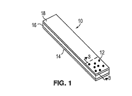
FIG. 1 is a perspective view of a portion of the light output side of a light
sheet 10,
showing a simplified pseudo-random pattern of LED areas 12. The LED areas 12
may instead be
in an ordered pattern. There may be 1,000 or more low power LEDs in a full
size 2x4 foot light
sheet to generate the approximately 3700 lumens (per the DOE CALiPER benchmark
test)
needed to replace a standard fluorescent fixture typically found in offices.
The light sheet of the present invention comprises a plurality of LEDs. The
LEDs have a
diameter from about 5 microns to about 80 microns, alternatively from about 5
microns to about
70 microns, alternatively from about 10 microns to about 60 microns,
alternatively from about 15
microns to about 50 microns, alternatively from about 20 microns to about 40
microns,
alternatively from about 15 microns to about 35 microns, alternatively
combinations thereof. In
one embodiment, the LEDs have a thickness less than 85 microns, alternatively
less than about
80 microns, alternatively from about 5 microns to about 80, alternatively from
about 10 microns
to about 70 microns, alternatively from about 15 microns to about 60 microns,
alternatively
combinations thereof. In yet another embodiment, the LED is less than 80
microns in any
dimension, alternatively less than 75 microns in any dimension, alternatively
less than 70
microns in any dimension.
The dimensions of the diodes may be measured using, for example, a scanning
electron
microscope (SEM), or Horiba's LA-920. The Horiba LA-920 instrument uses the
principles of
low-angle Fraunhofer Diffraction and Light Scattering to measure the LED size
and distribution
in a laminate of the present invention.
In one embodiment, the lighted sheet of the present invention comprises from
about 5 to
about 500 micro LEDs are disposed per 1 cm2of planar area of the laminate,
alternatively from
about 10 to about 200 micro LEDs are disposed, alternatively from about 15 to
about 150 micro
LEDs are disposed, alternatively from about 25 to about 125 micro LEDs are
disposed,
CA 02862348 2014-07-22
WO 2013/116623
PCT/US2013/024312
14
alternatively from about 35 to about 110 micro LEDs are disposed,
alternatively from about 45 to
about 100 micro LEDs are disposed, alternatively from about 60 to about 100,
micro LEDs are
disposed, alternatively from about 70 to about 90 microLEDs are disposed,
alternatively about 80
to about 90 micro LEDs are disposed per 1 cm2 of planar area of the laminate,
alternatively
combinations thereof.
In yet another aspect of the invention, the lighted sheet of the present
invention comprises
a plurality of micro LEDs comprising a planar area from about 0.005% to about
0.5% relative to
the planar area of the lighted sheet, alternatively from about 0.01% to about
0.1%, alternatively
from about 0.01% to about 0.3%, alternatively combinations thereof.
LEDs are well known. Suppliers of LED may include NthDegree Technologies;
Cree;
Osram; and Nichia, or any number of other LED suppliers. In an exemplary
embodiment, each
diode of the plurality of diodes comprises GaN and a silicon or sapphire
substrate. In another
exemplary embodiment, each diode of the plurality of diodes comprises a GaN
heterostructure
and GaN substrate. In various exemplary embodiments, the GaN portion of each
diode of the
plurality of diodes is substantially lobed, stellate, or toroidal.
In an exemplary embodiment, the plurality of diodes comprises at least one
inorganic
semiconductor selected from the group consisting of: silicon, gallium arsenide
(GaAs), gallium
nitride (GaN), GaP, InAlGaP, InAlGaP, AlinGaAs, InGaNAs, and AlInGASb. In
another
exemplary embodiment, the plurality of diodes comprises at least one organic
semiconductor
selected from the group consisting of: IT-conjugated polymers,
poly(acetylene)s, poly(pyrrole)s,
poly(thiophene)s, polyanilines, polythiophenes, poly(p-phenylene sulfide),
poly(para-phenylene
vinylene)s (PPV) and PPV derivatives, poly(3-alkylthiophenes), polyindole,
polypyrene,
polycarbazole, polyazulene, polyazepine, poly(fluorene)s, polynaphthalene,
polyaniline,
polyaniline derivatives, polythiophene, polythiophene derivatives,
polypyrrole, polypyrrole
derivatives, polythianaphthene, polythianaphthane derivatives,
polyparaphenylene,
polyparaphenylene derivatives, polyacetylene, polyacetylene derivatives,
polydiacethylene,
polydiacetylene derivatives, polyparaphenylenevinylene, polyp
araphenylenevinylene derivatives,
polynaphthalene, polynaphthalene derivatives, polyisothianaphthene (PITN),
polyheteroarylenvinylene (ParV) in which the heteroarylene group is thiophene,
furan or pyrrol,
polyphenylene-sulphide (PPS), polyperinaphthalene (PPN), polyphthalocyanine
(PPhc), and their
derivatives, copolymers thereof and mixtures thereof.
Examples of inorganic semiconductors may include, without limitation: silicon,
germanium, and mixtures thereof; titanium dioxide, silicon dioxide, zinc
oxide, indium-tin oxide,
CA 02862348 2014-07-22
WO 2013/116623
PCT/US2013/024312
antimony-tin oxide, and mixtures thereof; II-VI semiconductors, which are
compounds of at least
one divalent metal (zinc, cadmium, mercury and lead) and at least one divalent
non-metal
(oxygen, sulfur, selenium, and tellurium) such as zinc oxide, cadmium
selenide, cadmium
sulfide, mercury selenide, and mixtures thereof; III-V semiconductors, which
are compounds of
5 at least one trivalent metal (aluminum, gallium, indium, and thallium)
with at least one trivalent
non-metal (nitrogen, phosphorous, arsenic, and antimony) such as gallium
arsenide, indium
phosphide, and mixtures thereof; and group IV semiconductors including
hydrogen terminated
silicon, carbon, germanium, and alpha-tin, and combinations thereof.
Diodes are also described in U.S. Pat. No. 7,799,699 B2.
10
Referring to Figure 1, the pseudo-random pattern may repeat around the light
sheet 10
(only the portion within the dashed outline is shown). A pseudo-random pattern
is preferred over
an ordered pattern since, if one or more LEDs fail or have a poor electrical
connection, its
absence will be significantly harder to notice. The eye is drawn to defects in
an ordered patterns
where spacings are consistent. By varying the spacing in a pseudo-random
pattern such that
15 overall light uniformity is achieved and where there may be a low
amplitude variation in
luminance across the surface of the fixture, then the loss of any one LED
would not be perceived
as a break in the pattern but blend in as a small drop in local uniformity.
Typical viewers are
relatively insensitive to local low gradient non-uniformities of up to 20% for
displays. In
overhead lighting applications, the tolerable levels are even higher given
that viewers are not
prone to staring at fixtures, and the normal angle of view is predominantly at
high angles from
the normal, where non-uniformities will be significantly less noticeable.
An ordered pattern may be appropriate for applications where there is a
substantial
mixing space between the light sheet and the final tertiary optical system
which would obscure
the pattern and homogenize the output adequately. Where this would not be the
case and there is
a desire to have a thinner profile fixture, then the pseudo random pattern
should be employed.
Both are easily enabled by the overall architecture.
Alternatively, a variably ordered pattern of LED areas 12 may modulate across
the light
sheet 10.
The light sheet 10 is generally formed of three main layers: a bottom
substrate 14 having
an electrode and conductor pattern; an intermediate sheet 16 acting as a
spacer and reflector; and
a transparent top substrate 18 having an electrode and conductor pattern. The
LED chips are
electrically connected between electrodes on the bottom substrate 14 and
electrodes on the top
substrate 18. The light sheet 10 is very thin, such as a few millimeters, and
is flexible.
CA 02862348 2014-07-22
WO 2013/116623 PCT/US2013/024312
16
In one embodiment of the invention, the light sheet of the present invention
is a thickness
less than lmm, alternatively from about 0.1 mm to less than lmm, alternatively
from about 0.1
mm to about 0.8 mm, alternatively from about 0.1 mm to about 0.5 mm,
alternatively from about
0.15 mm to about 0.35 mm, alternatively less than about 0.5 mm, alternatively
less than bout 0.4
mm, alternatively less than bout 0.3 mm, alternatively from about 0.20 mm to
about 0.30 mm,
alternatively combinations thereof.
FIG. 2 is a perspective view of a portion of the underside of the light sheet
10 showing
the electrode and conductor pattern on the bottom substrate 14, where, in the
example, the LED
chips in the LED areas 12 are connected as two groups of parallel LEDs that
are connected in
series by conductors not shown in FIG. 2. The series connections may be by
vias through the
light sheet layers or through switches or couplings in the external connector
22. A conductor
pattern is also formed on the top substrate 18 for connection to the LED chips
top electrodes.
The customizable interconnection of the LED chips allows the drive voltage and
current to be
selected by the customer or requirements of the design. In one embodiment,
each identical group
of LED chips forms a series-connected group of LED chips by the conductor
pattern and the
external interconnection of the conductors, and the various groups of series
connected LED chips
may then be connected in parallel to be driven by a single power supply or
driven by separate
power supplies for high reliability. In yet another embodiment, the LED chips
could be formed
into a series-parallel connected mesh with additional active components as may
be needed to
distribute current amongst the LEDs in a prescribed fashion.
In one embodiment, to achieve a series connection of LED chips using top and
bottom
conductors, some LEDs chips are mounted on the bottom substrate with their
anodes connected
to the bottom substrate electrodes and other LED chips are mounted with their
cathodes
connected to the bottom electrodes. Ideally, adjacent LED chips are reversely
mounted to
simplify the series connection pattern. The conductor between the electrodes
then connects the
LED chips in series. A similar conductor pattern on the top substrate connects
the cathodes of
LED chips to the anodes of adjacent LED chips.
An DC or AC power supply 23 is shown connected to the connector 22. An input
of the
power supply 23 may be connected to the mains voltage. If the voltage drop of
an LED series
string is sufficiently high, the series string of LEDs may be driven by a
rectified mains voltage
(e.g., 120 VAC).
CA 02862348 2014-07-22
WO 2013/116623 PCT/US2013/024312
17
In another embodiment, it is also possible to connect the LED chips in two
anti-parallel
series branches, or derivatives thereof, that will enable the LED chips to be
driven directly from
AC, such as directly from the mains voltage.
FIGS. 3-5, 7, 8, 10-14, and 16-19 are cross-sectional views along line 3-3 in
FIG. 1,
cutting across two LED areas 12, showing the light sheet at various stages of
fabrication and
various embodiments.
FIG. 3A shows a bottom substrate 14, which may be a commercially available and
customized flex circuit. Any suitable material may be used, including thin
metals coated with a
dielectric, polymers, glass, or silicones. KaptonTM flex circuits and similar
types are commonly
used for connecting between printed circuit boards or used for mounting
electronic components
thereon. The substrate 14 has an electrically insulating layer 26, a patterned
conductor layer 28,
and metal electrodes 30 extending through the insulating layer 26. The
electrodes 30 serve as
heat sinking vias. Flexible circuits with relatively high vertical thermal
conductivities are
available. The substrate 14 is preferably only a few mils thick, such as 1-5
mils (25-125
microns), but may be thicker (e.g., up to 3 mm) for structural stability. The
conductor layer 28
may be plated copper or aluminum. The electrodes 30 are preferably copper for
high electrical
and thermal conductivity. The conductor layer 28 may instead be formed on the
top surface of
the substrate 14.
The conductor layer 28 may be any suitable pattern, such as for connecting the
LED chips
in series, parallel, or a combination, depending on the desired power supply
voltage and current,
and depending on the desired reliability and redundancy.
FIG. 3B illustrates another embodiment of a bottom substrate 32, which has a
metal
reflective layer 34 (e.g., aluminum) sandwiched between a top insulating layer
36 and a bottom
insulating layer 38. A conductor layer 40 and electrodes 42 are formed over
the top insulating
layer 36. The thickness of the bottom substrate 32 may be 1-5 mils, or
thicker, and flexible.
FIG. 3C illustrates another embodiment of a bottom substrate 44, which has a
dielectric
reflective layer 46. This allows the heat conducting metal electrodes 47 to be
formed through the
reflective layer 46. A conductor layer 48 is formed on the bottom of the
substrate, but may
instead be formed on the top surface of the substrate. An optional insulating
layer 50 overlies the
reflective layer 46.
Suitable sheets having a reflective layer may be MIRO IVTM, Vikuiti DESRTM, or
other
commercially available reflective sheets.
CA 02862348 2014-07-22
WO 2013/116623 PCT/US2013/024312
18
In one embodiment, components of the drive circuitry may be patterned directly
on the
bottom substrate 44 to avoid the need for separate circuits and PCBs.
FIG. 4 illustrates a conductive adhesive 52, such as epoxy infused with
silver, applied
over the electrodes 30. Such a conductive adhesive 52 simplifies the LED chip
bonding process
and increases reliability. Any of the bottom substrates described herein may
be used, and only the
bottom substrate 14 of FIG. 3A is used in the examples for simplicity.
FIG. 5 illustrates commercially available, non-packaged blue LED chips 56
being affixed
to the bottom substrate 14 by a programmed pick-and-place machine or other
prescribed die
placement method. The LED chips 56 have a small top electrode 58 (typically
used for a wire
bond) and a large bottom electrode 60 (typically reflective). Instead of a
conductive adhesive 52
(which may be cured by heat or UV) affixing the bottom electrode 60 to the
substrate electrode
30, the bottom electrode 60 may be ultrasonically welded to the substrate
electrode 30, solder
reflowed, or bonded in other ways. Suitable GaN LED chips 56 with a vertical
structure are sold
by a variety of manufacturers, such as Cree Inc., SemiLEDs, Nichia Inc., and
others. Suitable
Cree LEDs include EZ 290 Gen II, EZ 400 Gen II, EZ Bright II, and others.
Suitable SemiLEDs
LEDs include the SL-V-B15AK.
In one embodiment, the LEDs have have a top area of less than100 x 100
microns,
alternatively less than about 90 x 90 microns; and a have a thickness of less
than 85-microns,
alternatively less than a about 80 microns, alternatively from about 10
microns to about 75
microns, alternatively combinations thereof. The specifications for some
suitable commercially
available blue LEDs, in combination with phosphors to create white light,
identify a lumens
output in the range of 5-7 lumens per LED at a color temperature of about
4,100K. Suppliers
of LED may include NthDegree Technologies; Cree; Osram; and Nichia, or any
number of other
LED suppliers.
Other types of LED chips are also suitable, such as LED chips that do not have
a top
metal electrode for a wire bond. Some suitable LED chips may have a
transparent top electrode
or other electrode structures.
FIG. 6 is a perspective view of a transparent intermediate sheet 64 having
holes 66 for the
LED chips 56. Although the LED chips 56 themselves may have edges on the order
of 0.3 mm,
the holes 66 should have a much larger opening, such as 2-5 mm, alternatively
from 0.1 to 1 mm,
to receive a liquid encapsulant and sufficient phosphor to convert the blue
light to white light or
light with red and green, or yellow, components. The thickness of the
intermediate sheet 64 is
approximately the thickness of the LED chips 56 used, since the intermediate
sheet 64 has one
CA 02862348 2014-07-22
WO 2013/116623 PCT/US2013/024312
19
function of preventing excess downward pressure on the LED chips 56 during
lamination.
Transparent sheets formed of a polymer, such as PMMA, or other materials are
commercially
available in a variety of thicknesses and indices of refraction.
In one embodiment, the bottom surface of the intermediate sheet 64 is coated
with a
reflective film (e.g., aluminum) to provide a reflective surface. The
intermediate sheet may also
optionally have a further coating of dielectric to prevent electrical contact
with traces and to
prevent oxidation during storage or handling.
To adhere the intermediate sheet 64 to the bottom substrate 14, the bottom
surface of the
intermediate sheet 64 may be coated with a very thin layer of silicone or
other adhesive material.
The silicone may improve the total internal reflection (TIR) of the interface
by selection of a
suitably low index of refraction relative to the intermediate sheet 64.
FIG. 7 illustrates the intermediate sheet 64 having been laminated over the
bottom
substrate 14 under pressure. Heat may be used to cure the silicone. The
thickness of the
intermediate sheet 64 prevents a potentially damaging downward force on the
LED chips 56
during lamination.
In one embodiment, the intermediate sheet 64 is molded to have prisms 70
formed in its
bottom surface for reflecting light upward by TIR. If the bottom surface is
additionally coated
with aluminum, the reflection efficiency will be improved. Instead of, or in
addition to, a prism
pattern, the bottom surface may be roughened, or other optical elements may be
formed to reflect
the light through the light output surface.
FIG. 8A illustrates the area 12 surrounding the LED chips 56 filled with a
silicone/phosphor mixture 72 to encapsulate the LED chips 56. The mixture 72
comprises
phosphor powder in a curable liquid silicone or other carrier material, where
the powder has a
density to generate the desired amount of R, G, or Y light components needed
to be added to the
blue light to create a white light having the desired color temperature. A
neutral white light
having a color temperature of 3700-5000K is preferred. The amount/density of
phosphor required
depends on the width of the opening surrounding the LED chips 56. One skilled
in the art can
determine the proper types and amounts of phosphor to use, such that the
proper mixture of blue
light passing through the phosphor encapsulant and the converted light
achieves the desired white
color temperature. The mixture 72 may be determined empirically. Suitable
phosphors and
silicones are commercially available. The mixture 72 may be dispensed by silk
screening, or via
a syringe, or by any other suitable process. The dispensing may be performed
in a partial vacuum
CA 02862348 2014-07-22
WO 2013/116623 PCT/US2013/024312
to help remove any air from the gap around and under the LED chips 56. The
conductive
adhesive 52 (FIG. 4) helps fill in air gaps beneath the LED chips 56.
In another embodiment, the phosphor around the LED chips 56 in the holes may
be
preformed and simply placed in the holes around the LED chips 56.
5 Instead of the intermediate sheet 64 having holes with straight sides,
the sides may be
angled or be formed as curved cups such that reflectance of light outwards is
enhanced.
FIG. 8B illustrates the area surrounding the LED chips 56 filled with the
silicone/phosphor mixture 72, where the holes 74 in an intermediate sheet 76
are tapered to
reflect light toward the light output surface of the light sheet.
10 All the various examples may be suitably modified if the phosphor is
provided by the
LED manufacturer directly on the LED chips 56. If the LED chips 56 are pre-
coated with a
phosphor, the encapsulant may be transparent silicone or epoxy.
Even if the LED chips 56 are not perfectly centered within a hole 66/74, the
increased
blue light passing through a thin phosphor encapsulant will be offset by the
decreased blue light
15 passing through the thicker phosphor encapsulant.
FIG. 8C illustrates an intermediate sheet 78 molded to have cups 80
surrounding each
LED chip 56, where a reflective layer 82 (e.g., aluminum with an insulating
film over it) is
formed over the sheet 78 to reflect light toward the light output surface of
the light sheet. In the
embodiment shown, the cups 80 are filled with a silicone encapsulant 84 rather
than a
20 silicone/phosphor mixture, since a phosphor tile will be later affixed
over the entire cup to
convert the blue light to white light. In another embodiment, the cups 80 may
be filled with a
silicone/phosphor mixture.
FIG. 8D illustrates an embodiment where the intermediate sheet 85 is formed of
a
phosphor or is infused with a phosphor powder, or any other wavelength
conversion material. For
example, the intermediate sheet 85 may be a molded silicone/phosphor mixture.
Since the light
generated by phosphor widely scatters, the prisms 70 used in other embodiments
may not be
needed.
FIG. 8E illustrates that the LED chips 56 may be pre-coated with phosphor 86
on any
sides of the chips, such as on all light-emitting sides or only on the sides
and not on the top
surface. If the top surface is not coated with a phosphor, such as to not
cover the top electrode,
the blue light emitted from the top surface may be converted by a remote
phosphor overlying the
LED chip 56.
CA 02862348 2014-07-22
WO 2013/116623
PCT/US2013/024312
21
FIG. 9 is a perspective view of a transparent top substrate 88 having
electrodes 90 and a
conductor layer 92 formed on its bottom surface. The electrodes 90 may be
reflective (e.g.,
silver) or transparent (e.g., ITO). The top substrate 88 may be any clear flex
circuit material,
including polymers. The top substrate 88 will typically be on the order of 1-
20 mils thick (25
A thin layer of silicone may be silk-screened, sprayed with a mask, or
otherwise formed
on the bottom surface of the top substrate 88 for affixing it to the
intermediate sheet 64. The
electrodes 90 are preferably not covered by any adhesive in order to make good
electrical contact
with the LED chip electrodes 58.
FIG. 10 illustrates a conductive adhesive 94 (e.g., silver particles in epoxy
or silicone)
dispensed over the top electrodes 58 of the LED chips 56.
FIG. 11 illustrates the transparent top substrate 88 laminated over the LED
chips 56,
using pressure and heat. Heat is optional, depending on the type of curing
needed for the various
adhesives. A roller 96 is shown for applying uniform pressure across the light
sheet as the light
The thickness of the completed light sheet may be less than 1 mm resulting in
little
optical absorption and heat absorption. In one embodiment of the invention,
the complete light
30 For
added structural robustness, the light sheet can be made thicker. If
additional optics
are used, such as certain types of reflecting cups and light-shaping layers,
the total thickness can
become up to 1 cm and still maintain flexibility. The structure is cooled by
ambient air flow over
CA 02862348 2014-07-22
WO 2013/116623 PCT/US2013/024312
22
its surface. Any of the substrates and intermediate sheets described herein
can be mixed and
matched depending on the requirements of the light sheet.
FIGS. 12A-12D illustrate various phosphor conversion techniques that can be
used to
create white light. If UV LED chips are used, an additional phosphor
generating a blue light
component would be used.
FIG. 12A illustrates the LED chips side light being converted to red and green
light, or
yellow light, or white light and reflected through the light output surface of
the light sheet, while
the blue light from the LED chips 56 is directly transmitted through the
transparent electrode 100
on the transparent sheet 88 for mixing with the converted light a short
distance in front of the
light sheet. An observer would perceive the light emitted by the light sheet
as being substantially
uniform and white.
FIG. 12B illustrates all the light from the LED chips 56 being emitted from
the side due
to a reflective electrode 104 on the top transparent sheet 88 overlying the
LED chips 56. All light
is then converted to white light by the phosphor and reflected through the
light output surface of
the light sheet.
FIG. 12C illustrates side light being converted to white light by the phosphor
surrounding
the LED chips 56, and the blue top light, emitted through the transparent
electrode 100, being
converted to white light by a remote phosphor layer 106 formed on the top
surface of the top
substrate 88 over the LED chips 56. The phosphor layer 106 may be flat or
shaped. The area of
FIG. 12D illustrates the LED chips 56 being positioned in reflective cups 80
filled with a
roughened top or bottom surface for increasing the extraction of light and
providing a broad
spread of light. The roughening may be by molding, casting, or micro bead
blasting.
CA 02862348 2014-07-22
WO 2013/116623 PCT/US2013/024312
23
In another embodiment, shown in FIG. 13, the LED chips 112 may be flip chips,
with
anode and cathode electrodes 114 on the bottom surface of the LED chips 112.
In such a case, all
conductors 116 and electrodes 118 would be on the bottom substrate 120. This
would greatly
simplify the series connection between LED chips, since it is simple to design
the conductors 116
to connect from a cathode to an anode of adjacent LED chips 112. Having all
electrodes on the
bottom substrate 120 also improves the reliability of electrical connections
of the substrate
electrodes to the LED electrodes since all bonding may be performed
conventionally rather than
by the lamination process. The top substrate 122 may then be simply a clear
foil of any thickness.
The top substrate 122 may employ the reflectors (from FIG. 12B) above each LED
chip 112 for
causing the chips to only emit side light, or a phosphor layer 124 can be
positioned on the
substrate 122 above each LED chip 112 for converting the blue light into white
light, or any of
the other phosphor conversion techniques and intermediate sheets described
herein may be used
to create white light.
In another embodiment, LED chips are used where both electrodes are on the top
of the
chip, where the electrodes are normally used for wire bonding. This is similar
to FIG. 13 but
where the LEDs are flipped horizontally and the conductors/electrodes are
formed on the top
substrate 122. The bottom substrate 120 (FIG. 13) may contain metal vias 118
for heat sinking,
where the vias 118 are bonded to a bottom of the LED chips to provide a
thermal path between
the LED chips and the metal via 118 surface exposed on the bottom surface of
the bottom
substrate. The chips can then be air cooled. A thermally conductive adhesive
may be used to
adhere the LED chips to the vias 118.
FIG. 14 illustrates LED chips 56 that are alternately mounted on the bottom
substrate 14
so that some have their cathode electrodes 60 connected to the bottom
substrate electrodes 30 and
some have their anode electrodes 58 connected to the bottom substrate
electrodes 30. The top
substrate 88 transparent electrodes 134 then connect to the LED chips other
electrodes. Since the
LED chips' cathode electrode 60 is typically a large reflector, the LED chips
connected with their
cathodes facing the light output surface of the light sheet will be side
emitting. The electrodes 30
on the bottom substrate 14 are preferably reflective to reflect light upward
or sideward. The
connectors 136 on the top substrate 88 and the connectors 138 on the bottom
substrate 14 can
then easily connect the adjacent LED chips in series without any vias or
external connections.
For converting the top blue light from some LED chips to white light, a
phosphor layer 142 may
be used above the LED chips.
CA 02862348 2014-07-22
WO 2013/116623 PCT/US2013/024312
24
FIGS. 15-18 illustrate other embodiments that better enable the LED chips 56
to be
connected in series within the light sheet 10.
FIG. 15 illustrates an intermediate sheet 150 having square holes 152 with
metal
electrodes 154 and 156 formed on opposing walls of the holes 152, where the
electrode metal
wraps around a surface of the intermediate sheet 150 to be contacted by a
conductor pattern on
the surface of the intermediate sheet 150 or one or both of the top substrate
or bottom substrate.
The electrodes may be formed by printing, masking and sputtering, sputtering
and etching, or by
other known methods.
As shown in FIG. 16, the LED chips 56, with top and bottom electrodes, are
then inserted
vertically in the holes 152 so that the LED electrodes 58 and 60 contact the
opposing electrodes
154 and 156 formed on the walls of the holes 152. The electrodes 154 and 156
may be first
coated with a conductive adhesive, such as silver epoxy, to ensure a good
contact and adhesion.
The intermediate sheet 150 has about the same thickness of the chips 56, where
the thickness of
the chips 56 is measured vertically. This helps protect the chips 56 from
physical damage during
lamination.
In the example of FIG. 16, the electrodes 154 and 156 extend to the bottom
surface of the
intermediate sheet 150 for being interconnected by conductors 158 formed on
the bottom
substrate 160. In one embodiment, the bottom substrate 160 has a metal
reflector layer on its
bottom surface or internal to the substrate for reflecting the side light back
up though the light
output surface of the light sheet. The reflective layer may also be a
dielectric layer.
The conductors 158 in FIG. 16 connect the anode of one LED chip 56 to the
cathode of
an adjacent LED chip 56. The conductors 158 may additionally connect some
series strings in
parallel (or connect parallel LED chips in series).
FIG. 17 illustrates two light rays generated by the LED chip 56 being
reflected by the
LED chip's bottom reflective electrode 60 and the reflective electrode 154 or
reflective scattering
conductive adhesive. Since the bottom substrate 160 also has a reflector, all
light is forced
through the top of the light sheet.
Any air gaps between the LED chips 56 and the holes 152 may be filled in with
a suitable
encapsulant that improves extraction efficiency.
A phosphor layer 162 converts the blue light to white light.
FIGS. 16 and 17 also represent an embodiment where the conductor pattern is
formed
directly on the bottom or top surface of the intermediate sheet 150, so all
electrodes and
conductors are formed on the intermediate sheet 150. No top substrate is
needed in these
CA 02862348 2014-07-22
WO 2013/116623 PCT/US2013/024312
embodiments, although one may be desired to seal the LED chips 56.
FIG. 18 illustrates an embodiment where the conductors 166 and 168 are formed
on both
sides of the intermediate sheet 150 or formed on the transparent top substrate
170 and bottom
substrate 160. The LED chips 56 can easily be connected in any combination of
series and
5 parallel.
FIGS. 19A and 19B represent an embodiment where the bottom substrate 176 has
conductors 178 formed on its top surface. The bottom electrodes (e.g.,
cathodes) of the LED
chips 56 are bonded to the conductors 178. For a series connection between LED
chips 56, solid
metal interconnectors 180 are also bonded to the conductors 178. The
intermediate sheet 182 has
10 holes that correspond to the LED chip 56 locations and interconnector
180 locations, and the tops
of the chips 56 and interconnectors 180 are approximately planar with the top
of the intermediate
sheet 182. The areas surrounding the LED chips 56 may be filled in with a
phosphor/silicone
mixture 72.
In FIG. 19B, a transparent top substrate 184 has anode conductors 186 that
interconnect
15 the anode electrodes of LED chips 56 to associated interconnectors 180
to create a series
connection between LED chips 56. This series interconnection technique may
connect any
number of LED chips 56 in series in the sheet or strip. A pick and place
machine is simply
programmed to place an LED chip 56 or an interconnector 180 at selected
locations on the
bottom substrate 176. The bonding may be performed by ultrasonic bonding,
conductive
20 adhesive, solder reflow, or any other technique. Alternatively, LEDs are
printed to form the light
sheet, preferably wherein the printing is selected from screen printing,
flexographic printing, or
rotogravure printing.
The interconnector 180 may also be a plating of the hole in the intermediate
sheet 182 or
a soft conductor paste that is injected into the hole, printed within the
hole, etc.
25 A phosphor layer or tile 188 may be affixed on the top substrate 184
over the LED chips 56 to
convert the blue light emitted from the top surface of the chips 56 to white
light. If the phosphor
layer/tile 188 was large enough, then phosphor need not be used in the
encapsulant.
The bottom substrate 176 may have a reflective layer either imbedded in it or
on its
bottom surface, as previously described, for reflecting light toward the light
output surface.
In a related embodiment, the hole for the interconnector may be formed
completely
through the light sheet, then filled with a metal or coated with a metal. The
hole may be formed
using a laser or other means. The metal may be a printed solder paste that is
reflowed to make
electrical contact to the conductors formed on the substrates to complete the
series connection.
CA 02862348 2014-07-22
WO 2013/116623 PCT/US2013/024312
26
Extending the metal external to the light sheet will improve heat sinking to
ambient air or to an
external heat sink material. If the metal has a central hole, cooling air may
flow through it to
improve heat sinking.
FIGS. 20-31 illustrate various embodiments where there is no intermediate
sheet or strip.
In FIGS. 20A and 20B, the bottom substrate 190 has cavities 192 molded in it
or grooves
molded in it. Grooves may also be formed by extruding, machining, or injection
molding the
substrate 190. The width of the bottom substrate 190 may be sufficient to
support one, two, three
Cathode conductors 194 are formed on the bottom substrate 190 and are bonded
to the
cathode electrodes of the vertical LED chips 56.
A top substrate 196 has anode conductors 198 that are aligned with the anode
electrodes
FIG. 20B shows the top substrate 196 laminated onto the bottom substrate 190.
A thin
Instead of the groove or cavity being formed in the bottom substrate 190, the
groove or
FIG. 20C is a transparent top down view of FIG. 20B illustrating one possible
conductor
pattern for the conductors 194 and 198, where the LED chips 56 are connected
in series, and two
CA 02862348 2014-07-22
WO 2013/116623 PCT/US2013/024312
27
sets of series-connected LED strings are shown within the laminated
substrates. The anode
conductors 198 above the LED chips 56 are narrow to block a minimum amount of
light. The
various metal conductors in all embodiments may be reflective so as not to
absorb light. Portions
of the anode conductors 198 over the LED chips 56 may be transparent
conductors.
As shown in FIG. 20D, any number of LED chips 56 may be connected in series in
a strip
or sheet, depending on the desired voltage drop. Three series strings of LED
chips 56 in a single
strip or sheet are shown in FIG. 20D, each series string being connected to a
controllable current
source 202 to control the string's brightness. The LED chips 56 are offset so
as to appear to be in
a pseudo-random pattern, which is aesthetically pleasing and makes a failed
LED chip not
noticeable. If there is sufficient diffusion of the light, each string of LED
chips may create the
same light effect as a fluorescent tube. A cathode connector and an anode
connector may extend
from each strip or sheet for coupling to a power supply 204 or to another
strip or sheet. This
allows any configuration of series and parallel LED chips.
In all the embodiments described herein, metal slugs may be provided that
extend through
the bottom substrate so as to provide a metal heat path between the bottom
electrodes of the LED
chips and air. The slugs may be similar to the electrodes 30 in FIGS. 3A-5 but
may be electrically
insulated from other slugs or electrically connected to the electrodes of
other LEDs by a
conductor layer for a series connection. A thin dielectric may separate the
LED electrodes from
the slugs if the slugs are to be electrically floating.
FIGS. 21A, 21B, and 21C illustrate a different configuration of cathode
conductors 206
and anode conductors 208 on a bottom substrate 210 and top substrate 212 for
connecting the
LED chips 56 in series when the substrates are brought together. In FIGS. 21A-
C, there is only
one LED chip 56 mounted along the width of the structure, and the flexible
structure can be any
length depending on the number of LED chips to connect in series and the
desired distance
between LED chips 56. In FIG. 21C, the LED chip 56 may be encapsulated in
silicone or a
phosphor/silicone mixture, and a phosphor tile or phosphor layer 214 is
affixed over the LED
chip 56 to generate white light. The phosphor layer 214 may be deposited over
the entire top
surface of the top substrate 212. The bottom substrate 210 has a reflective
layer 199.
FIG. 22 illustrates that the top substrate 216 may be hemispherical with a
phosphor layer
218 over the outer surface of the top substrate 216 for converting the blue
LED light to white
light. Silicone encapsulates the chip 56. By providing the top substrate 216
with a rounded
surface, there is less TIR and the emitted white light pattern is generally
lambertian. Also, for all
embodiments, shaping the top substrate can be used to shape the light emission
pattern. For
CA 02862348 2014-07-22
WO 2013/116623
PCT/US2013/024312
28
example, the top substrate shape can act as a lens to produce a batwing or
other non-lambertian
emission pattern for more uniform illumination.
The diameters/widths of the substrates in FIGS. 21-22 and the substrates
described below
may be on the order of less than 1 mm to limit light attenuation, to maintain
high flexibility, to
minimize the height of the light fixture, and to enable handling of the
substrates using
conventional equipment. The substrates can, however, be any size.
FIGS. 23A and 23B illustrate that the groove 220 or cavity for the LED chip 56
may be
formed in the top substrate 222 rather than in the bottom substrate 224.
In the various embodiments where the LED dies have a semicircular top
substrate, the
light emitted from the dies in the direction of the substrate surface less
than the critical angle is
transmitted through the surface. However, light emitted from the dies in the
direction of the top
substrate's length may be subject to more total internal reflection.
Therefore, such low angle light
or internally reflected light should be reflected toward the surface of the
top substrate by angled
prisms or other reflectors positioned between adjacent LED dies along the
length of the top
substrate to provide a uniform emission pattern along the length of the light
strip. The reflectors
may be formed in the top or bottom substrates similar to the prisms 70 shown
in FIG. 7.
The bottom substrate 224 may be widened to support any number of LED chips
along its
width, and a separate hemispherical top substrate 222 may be used to cover
each separate series
string of LED chips mounted on the single bottom substrate (shown in FIG. 25).
FIG. 24 is a schematic diagram representing that any number of LED chips 56
may be
connected in a series string 225 in the substrate structure of FIGS. 21-23.
FIG. 25 illustrates a support base 226 for the separate strings 225 of LED
chips 56. The
support base 226 may be a bottom substrate, such as substrates 210 or 224 in
FIGS. 21-23, or
may be a separate support base for strings 225 encased in the top and bottom
substrates shown in
FIGS. 21-23. Each string 225 may be controlled by a separate current source
230 and powered by
a single power supply voltage connected to the anodes of the strings 225. If
some strings output
light of a different chromaticity, or color temperature, the current applied
to the various strings
may be controlled to make the overall chromaticity, or color temperature, of
the light sheet a
target chromaticity, or color temperature. Many driving arrangements are
envisioned. In one
embodiment, the support base 226 is nominally 2x4 feet to be a replacement for
a 2x4 foot
standard ceiling fluorescent fixture. Since each series string 225 of LED
chips 56 is very thin,
any number of strings can be mounted on the support base 226 to generate the
required number
of lumens to substitute for a standard 2x4 foot fluorescent fixture.
CA 02862348 2014-07-22
WO 2013/116623 PCT/US2013/024312
29
FIGS. 26A-26C illustrate a variation of the invention, where the substrates
are connected
together when initially molded or extruded. One or both substrates may be
rounded.
In FIG. 26A, a bottom substrate 240 and a top substrate 242 are molded or
extruded
together and connected by a resilient narrow portion 244. This allows the top
substrate 242 to be
closed over the bottom substrate 240 and be automatically aligned. Cathode
conductors 246 and
anode conductors 248 are formed on the substrates 240 and 242 in the
arrangement shown in
FIG. 26B so that, when the substrates 240 and 242 are brought together, the
LED chips 56 are
connected in series. Silicone or a phosphor/silicone mixture may be used to
encapsulate the LED
chips 56, or the outer surface of the substrates is coated with a phosphor
layer to convert the blue
light to white light. Any number of LED chips 56 can be connected in series
within the
substrates.
FIG. 26C illustrates the resulting substrate structure affixed to a support
base 250. The
support base 250 may have a reflective groove 252 for reflecting light 254.
The groove 252 may
be repeated along the width of the support base 250 for supporting a plurality
of substrate
structures.
The bottom substrate 240 may have a flat bottom while the top substrate is
hemispherical.
This helps mounting the bottom substrate on a reflective support base.
Providing the top substrate
as hemispherical, with an outer phosphor coating, results in less TIR and a
more lambertian
emission.
In the various embodiments describing overlapping conductors on the top and
bottom
substrates forming a series connection, the connection may be enhanced by
providing solder
paste or a conductive adhesive on the conductor surfaces, followed by solder
reflow or curing.
FIG. 27 illustrates the use of an LED chip 256 that emits light through all
surfaces of the
chip. For example, its cathode electrode may be a small metal electrode that
contacts a
transparent (e.g., ITO) current spreading layer. Such a chip 256 is sandwiched
between two
substrates 258 and 260 that have anode and cathode connectors 262 and 264 that
contact the
chips electrodes and connect multiple chips in series, similar to the
embodiments of FIGS. 20-
26.
FIG. 28 illustrates an embodiment where the bottom substrate includes a
reflective layer
270, such as aluminum, a dielectric layer 272, and conductors 274. The LED
chips 56 are in
reflective cups 278, such as molded cups with a thin reflective layer
deposited in the cups. The
cups 278 may be formed in a separate intermediate sheet that is laminated
before or after the
LED chips 56 are affixed to the bottom substrate. Phosphor 280 fills the area
surrounding the
CA 02862348 2014-07-22
WO 2013/116623 PCT/US2013/024312
LED chips 56. In one embodiment, the phosphor 280 may fill the entire cup 278
so that the cup
278 itself is the mold for the phosphor 280. In another embodiment, some or
all of the light-
emitting surfaces of the LED chips 56 are coated with phosphor 280 prior to
the LED chips 56
being affixed on the bottom substrate.
5 The top substrate 282 has conductors 284 that contact the top electrodes
58 of the LED
chips 56, and the conductors 274 and 284 may come in contact with each other
using the various
techniques described herein to connect the LED chips 56 in series. The top
substrate 282 has
formed on its surface a phosphor layer 286 that converts the LED chips top-
emitted light to
white light. The top substrate 282 may have an optical layer 288 laminated
over it. The optical
In one embodiment, the bottom substrate of FIG. 28 is 1-2 mm thick, the cup
layer is 2-3
mm, the top substrate 282 is 1-2 mm, and the optical layer 288 is 2-3 mm,
making the overall
thickness about 0.6-1 cm.
15 FIG. 29 illustrates a portion of a light sheet with a repeating pattern
of strings of LED
chips 56. The view of FIG. 29 is looking into an end of a series string of LED
chips 56. A bottom
substrate 292 includes a reflective layer 294 and a dielectric layer 296.
Conductors 298 are
formed on the dielectric layer 296, and LED chip electrodes are electrically
connected to the
conductors 298.
20 A top substrate 300 has cavities or grooves 302 that extend into the
plane of FIG. 29 and
contain many LED chips 56 along the length of the light sheet. If the top
substrate 300 extends
across the entire light sheet, there would be many straight or meandering
grooves 302, where the
number of grooves depends on the number of LED chips used. The top substrate
300 has
conductors 304 that contact the top electrodes of the LED chips 56 and contact
the conductors
The portions of the top substrate 300 directly over the LED chips 56 have a
phosphor
CA 02862348 2014-07-22
WO 2013/116623 PCT/US2013/024312
31
may extend across an entire 2x4 foot light sheet. Alternatively, there may be
a separate top
substrate for each string of LED chips 56.
At the end of each series string of LED chips or at other points in the light
sheet, the
anode and cathode conductors on the substrates must be able to be electrically
contacted for
connection to a current source or to another string of LED chips, whether for
a series or parallel
connection. FIGS. 30A, 30B, and 31 illustrate some of the many ways to
electrically connect to
the various conductors on the substrates.
FIG. 30A illustrates an end of a sheet or strip where the bottom substrate 310
extends
beyond the top substrate 312, and the ends of conductor 314 and 315 on the
bottom substrate 310
are exposed. Substrate 310 is formed of a reflective layer 311 and a
dielectric layer 313. FIG.
30B is a top down view of the end conductors 314 and 315 on the bottom
substrate 310 and an
end conductor 316 on the top substrate 312. The conductor 316 contacts the
anode electrode of
the LED chip 56 and contacts the conductor 315.
The ends of the exposed portions of the conductors 314 and 315 are thickly
plated with
copper, gold, silver, or other suitable material to provide connection pads
317 for solder bonding
or for any other form of connector (e.g., a resilient clip connector) to
electrically connect the
anode and cathode of the end LED chip 56 to another string or to a power
supply. The connection
pads 317 may be electrically connected to a connector similar to the connector
22 in FIG. 2 so
the connections to and between the various strings of LED chips 56 can be
determined by the
customized wiring of the connector 22 to customize the light sheet for a
particular power supply.
FIG. 31 is a side view of a portion of a light sheet showing plated connection
pads 318-
321 formed along the bottom substrate 324 that lead to conductors, such as
conductors 314 in
FIG. 30A, on the bottom substrate 324. Pads 318 and 319 may connect to the
anode and cathode
electrodes of an LED chip at the end of one string of LED chips, and pads 320
and 321 may
connect to the anode and cathode electrodes of an LED chip at the end of
another string of LED
chips. These pads 318-321 may be suitably connected to each other to connect
the strings in
series or parallel, or the strings may be connected to power supply terminals.
In one embodiment,
a string of LED chips consists of 18 LED chips to drop approximately 60 volts.
The pads 318-
321 may act as surface mounted leads soldered to a conductor pattern on a
support base, since
solder will wick up on the pads 318-321 while soldering to the conductor
pattern. The pads 318-
321 may also be connected using a resilient clip connector or other means. The
pads 318-321
may also extend to the bottom surface of the substrate 324 for a surface mount
connection.
CA 02862348 2014-07-22
WO 2013/116623 PCT/US2013/024312
32
In the various embodiments, the material for the substrates preferably has a
relatively
high thermal conductivity to sink heat from the low power LED chips. The
bottom substrates
may even be formed of aluminum with a dielectric between the conductors and
the aluminum.
The aluminum may be the reflector 199 in FIG. 20A or other figures. The
backplane on which
the LED/substrates are affixed may be thermally conductive.
The various conductors on the transparent top substrates may be metal until
proximate to
each LED chip, then the conductors become a transparent conductor (e.g., ITO)
directly over the
LED chip to not block light. A conductive adhesive (e.g., containing silver)
may be used to bond
the LED chips anode electrode to the ITO.
The wavelength converting material, such as phosphor, can be infused in the
top
substrate, or coated on the top substrate, or used in the LED chip's
encapsulant, or deposited
directly over the LED chip itself, or formed as a tile over the LED, or
applied in other ways.
The LED chips/substrate structures may be mounted on any suitable backplane
that may
include reflective grooves in a straight or meandering path. It is preferable
that the LED chips
appear to be in a pseudo-random pattern since, if an LED chip fails (typically
shorts), it will not
be noticeable to a viewer.
The top substrate may be molded with any optical pattern to shape the light
emission.
Such patterns include Fresnel lenses or holographic microstructures. Also, or
instead, an
additional optical sheet may be positioned in front of the substrate
structures for shaping the
light, such as diffusing the light, to meet the requirements of office
lighting directed by the
Illuminating Engineering Society of North America, Recommended Practice 1-
Office Lighting
(IESNA-RP1).
In addition, having a plurality of strips of LED chips, with the strips having
different
optical structures for different light emission patterns, could be used with a
controller that
controls the brightness of each strip to create a variable photometric output.
The number of LED chips, chip density, drive current, and electrical
connections may be
calculated to provide the desired parameters for total flux, emission shape,
and drive efficiency,
such as for creating a solid state light fixture to replace standard 2x4 foot
fluorescent fixtures
containing 2, 3, or 4 fluorescent lamps.
Since the substrates may be only a few millimeters thick, the resulting solid
state
luminaire may be less than 1 cm thick. This has great advantages when there is
no drop ceiling or
in other situations where space above the luminaire is limited or a narrow
space is desirable.
CA 02862348 2014-07-22
WO 2013/116623 PCT/US2013/024312
33
In embodiments where there is a conductor over the LED chip, a phosphor layer
may be
deposited on the inside surface of the substrate followed by an ITO deposition
over the phosphor
so that LED light passes through the ITO then excites the phosphor.
To avoid side light from the LED chips becoming scattered in the substrates
and
attenuated, 45 degree reflectors, such as prisms, may be molded into the
bottom substrate
surrounding each LED chip, similar to the prisms 70 in FIG. 7, to reflect
light toward the light
output surface of the light sheet.
Since the substrates are flexible, they may be bent in circles or arcs to
provide desired
light emission patterns.
Although adhesives have been describe to seal the substrates together, laser
energy, or
ultrasonic energy may also be used if the materials are suitable.
It is known that LED chips, even from the same wafer, have a variety of peak
wavelengths so are binned according to their tested peak wavelength. This
reduces the effective
yield if it is desired that the light sheet have a uniform color temperature.
However, by adjusting
the phosphor density or thickness over the various LED chips used in the light
sheet, many
differently binned LED chips can be used while achieving the same color
temperature for each
white light emission.
The LEDs used in the light sheet may be conventional LEDs or may be any type
of
semiconductor light emitting device such as laser diodes, etc. Work is being
done on developing
solid state devices where the chips are not diodes, and the present invention
includes such
devices as well.
Quantum dots are available for converting blue light to white light (the
quantum dots add
yellow or red and green components to create white light). Suitable quantum
dots can be used
instead of or in addition to the phosphors described herein to create white
light.
To provide high color rendering, the direct emissions of LED chips in the
light sheet
emitting red and green light can be controlled to mix with the white light
emitted by phosphor-
converted LED chips to produce a composite light that achieves high color
rendering and enables
the possibility of tuning the light by independent or dependent control of the
red and green LEDs
by open loop deterministic means or closed loop feedback means or any
combination thereof. In
one embodiment, different strings of LED chips have different combinations of
the red, green,
and phosphor-converted LEDs, and the strings are controlled to provide the
desired overall color
temperature and color rendering.
CA 02862348 2014-07-22
WO 2013/116623 PCT/US2013/024312
34
Since the light sheet is highly flexible and extremely light, it may be
retained in a
particular shape, such as flat or arced, using a light-weight frame.
FIG. 32 is a perspective view of a plastic frame 330 for supporting the
flexible light sheet
strip or sheet 10 by its edges or over other portions of its surface
(depending on the width of the
light sheet) to selectively direct light toward an area directly under the
light sheet. Other
configurations are achievable. Thin sheets containing optical elements for
further control of the
light emission from the light sheet may be supported by the frame 330.
In some applications, it may be desirable to have a luminaire emit light
generally
downward and off the ceiling for a certain lighting effect. Accordingly, all
the light sheet/strip
embodiments may be adapted to create a bidirectional sheet or strip.
Multiple light sheets may also be mounted in a ceiling fixture as flat strips,
and each strip
is tilted at a different angled relative to the floor so that the peak
intensities of the strips are at
different angles. In one embodiment, the peak intensity is normal to the flat
surface of the light
sheet, assuming no re-directing lenses are formed in the light sheet.
Therefore, the shape of the
light pattern from the fixture can be customized for any environment and can
be made to merge
with light from other fixtures. In one embodiment, some light strips are
angled downward at 55
degrees, and other light sheets are angled upward to reflect light off the
ceiling.
FIG. 33 illustrates LED dies 56 that are oppositely mounted in a light sheet
to create a
bidirectional emission pattern. This is similar to FIG. 14, but there is no
reflector covering the
entire bottom substrate. In FIG. 33, any number of LED dies 56 are connected
in series by
alternating the orientation of the LED dies along the light sheet to connect
the anode of one LED
die to the cathode of an adjacent LED die using metal conductors 340 and 342
formed on the top
substrate 344 and bottom substrate 346. The substrate electrodes contacting
the LED electrodes
58, formed on the light-emitting surface of the LED dies, may be transparent
electrodes 348 such
as ITO (indium-doped tin oxide) or ATO (antimony-doped tin oxide) layers. A
phosphor layer
350 may be deposited to generate white light from the blue LED emission.
FIG. 34 illustrates two light sheets back-to-back, similar to the light sheet
of FIG. 13, but
sharing a common middle substrate layer 351. The LED dies 352 are shown as
flip-chips, and the
conductor layers for interconnecting the LED dies on each side in series are
deposited on
opposite sides of the middle substrate 351. The light sheet structure is
sandwiched by transparent
substrates 356 and 358. The middle substrate 351 may include a reflective
layer that reflects all
impinging light back through the two opposite surfaces of the bidirectional
light sheet.
CA 02862348 2014-07-22
WO 2013/116623 PCT/US2013/024312
FIG. 35 is another example of two light sheets or strips, similar to the light
sheet
described with respect to FIG. 20B, affixed back-to-back with a middle
reflective layer 360. The
conductors 194 and 198 and substrates 196 and 190 are described with respect
to FIGS. 20A and
20B. The light sheets may be affixed to the middle reflective layer 360 using
a thin layer of
5 silicone or other adhesive. Phosphor (not shown) may be used to convert
the blue LED light to
white light.
The middle reflective layer 360 may have as a property that it is a good
conductor of
thermal energy which can assist the traces 194 in dissipating the heat from
the chips 56. There
may be enough thermal mass within the middle layer 360 that it provides all of
the heat sink
10 required to operate the chips safely or it may be extended laterally
(beyond the edges of the
substrates 190 and 196, shown in dashed outline) to regions where the heat may
be dissipated
more freely to the air within the lighting fixture.
Any of the light sheet/strip structures described herein may be adapted to
create a
bidirectional light sheet.
15 The light output surfaces of the various substrates may be molded to
have lenses, such as
Fresnel lenses, that customize the light emission pattern, such as directing
the peak intensity light
55 degrees off the normal, which is a desired angle to reduce glare and to
allow the light to merge
smoothly with light from an adjacent fixture. Different lenses may be formed
over different LED
dies to precisely control the light emission so as to create any spread of
light with selectable peak
20 intensity angle(s).
FIG. 36 illustrates a bidirectional light sheet 362 hanging from a ceiling
364. Light rays
366 are shown being reflected off the ceiling for a soft lighting effect,
while downward lighting
provides direct light for illumination. The light output surfaces of the light
sheet 362 may be
patterned with lenses, as described above, to create the desired effect. The
top and bottom light
25 emissions may be different to achieve different effects. For example, it
would be desirable for the
upward emitting light sheet to output the peak light emission at a wide angle
to achieve more
uniform lighting of the relatively proximate ceiling, while the downward
emitting light sheet
would emit light within a narrower range to avoid glare and cause the light to
smoothly merge
with light from an adjacent fixture. In one embodiment, the size of the light
sheet 362 is 2x4 feet;
30 however, the light sheet 362 can be any size or shape.
The top and bottom light emissions may also be adapted to have different
spectral
contents in addition to different optical dispersion characteristics. It is
advantageous in some
designs to consider that the soft fill light from above have one spectral
content such as the lighter
CA 02862348 2014-07-22
WO 2013/116623 PCT/US2013/024312
36
blue of daylight, for example 5600 Kelvin, and the direct light downwards
having a preferred
spectral content such as 3500 Kelvin, which mimics direct sunlight. The design
of light sheet 362
is well suited to the creation of these two components. Furthermore, the
modulation of light
levels from the top and bottom light emissions may differ temporally as in the
simulation of a
day lighting cycle or to favor background illumination over direct
illumination or in any
combination as may be desired by users to increase their comfort and
performance of tasks
within the space.
Alternatively, the bidirectional light sheet 362 may be mounted in a
conventional
diffusively reflective troffer.
In one embodiment, the ceiling panels above the fixture may be infused with
phosphor or
other wavelength conversion material to achieve a desired white point from the
ceiling light. In
such a case, the light sheet may direct UV or blue light toward the ceiling.
In some applications, it may be desirable to provide a bidirectional light
sheet emitting
low intensity up-light and higher intensity down light, or vice versa. In the
various disclosed
embodiments of unidirectional light sheets having a reflective layer, the
reflective layer may be
omitted so there is a primary light emission surface and an opposing light
leakage surface. The
light leakage may be useful in certain applications, such as illuminating a
ceiling to avoid a
shadow and decreasing luminance contrast ratios.
To avoid any manufacturing difficulties with lamination and alignment, the
snap-in
structure of FIG. 37A may be used. The LED die 368 is mounted on a trapezoidal
or frustum
shaped base substrate 370. The base substrate 370 can have many other shapes
that mate with a
corresponding mating feature in a top substrate 372. The base substrate 370
can be small and
support a single LED die 368 or may be a strip and support many LED dies
(e.g., 18) connected
in series. The conductor 374 connects to the die's top electrode 376, and the
conductor 378
connects to the die's bottom electrode 380 via the base substrate's conductor
382. The conductors
374 and 378 extend into the plane of the figure to create a series connection
between adjacent
LED dies (anode to cathode) along the length of the top substrate 372 one
example of which is
shown in FIG. 37B.
As seen in FIG. 37B, the conductor 374 connected to the LED's top (e.g.,
anode)
electrode 376 leads to the conductor 378 connected to the adjacent LED's
bottom (e.g., cathode)
electrode. The serpentine pattern continues to connect any number of LEDs
together. Many other
conductor patterns may be used to make the series connections. Alternatively,
the conductor
CA 02862348 2014-07-22
WO 2013/116623 PCT/US2013/024312
37
pattern used make the series connections may be formed on the snap-in strips
(supporting the
LED dies 368).
At least the top substrate 372 is formed of a resilient material, such as
transparent plastic
or silicone, so as to receive the base substrate 370 and resilient fix it in
place. The spring force
will provide a reliable compressive force between the opposing conductors, so
a conductive
adhesive between the abutting metal surfaces may be optional. The resulting
structure may
contain a string of LED dies that can be mounted on a larger support substrate
with other strings
of LED dies, or the top substrate 372 may extend laterally to receive multiple
strips of base
substrates 370, each supporting a series string of LED dies. The resulting
structure may resemble
that of FIG. 25, where the substrates can be any length and contain any number
of LED dies.
FIG. 37A shows the replication of identical top substrates 372 as part of a
single large substrate.
The top substrate 372 may be molded to have side reflectors 384 coated with a
reflector or with a
diffused reflector. The half-cylindrical top surface of the top substrate 372
may have a phosphor
layer 386 for generating white light. A remote optical sheet 388 may be molded
with optical
elements (e.g., prisms, lenses, etc.) to create any light emission pattern.
In one embodiment, the base substrate 370 is formed of a metal, such as
aluminum, with a
dielectric coating so that the base substrate 370 acts as a heat sink. Since
the back surface of the
base substrate 370 will be the highest part of the light sheet/strip when the
light sheet is mounted
in a ceiling or fixture, ambient air will cool the exposed surface of the
metal.
In the various snap-in embodiments, the top substrate may be flexed to open up
the edges
of the receiving cavity or groove to allow the die substrate to easily snap in
place. Alternatively,
the top substrate may be heated to the point of plastic deformation such that
the die substrate
could also be readily inserted and the assembly then allowed to cool thereby
locking the two
parts together.
An encapsulant may be deposited along the sides of the die, which then
squishes out
when the die substrate snaps in place to encapsulate the die and provide a
good index of
refraction interface between the die and the top substrate.
The die substrates may be formed as a strip, supporting a plurality of spaced
dies, or may
be formed to only support a single die.
FIG. 38 illustrates how a plurality of top substrates 372 may be snapped over
mating
features of a single bottom substrate 392 that is molded to create islands or
strips of snap-in
features 394, similar to those described with respect to FIG. 37A. Using such
snap-in techniques
automatically aligns the top and bottom substrates and simplifies the
electrical contacts for
CA 02862348 2014-07-22
WO 2013/116623 PCT/US2013/024312
38
forming serial strings of LEDs. The conductor pattern of FIG. 37B may be used
with all the snap-
in embodiments to connect the LED dies in series.
The phosphor layer 386 may be different for each serial column of LED chips so
that the
overall color temperature of the light sheet can be adjusted by changing the
brightness of the
various series strings of LED chips. For example, a thinner phosphor layer 386
will create bluer
light, and the brightness of the associated LED chips can be adjusted to make
the overall color
temperature higher or lower. Many variations can be envisioned where different
chromaticity of
each LED string phosphor layer 386 may be controlled to create tunable white
light.
In one embodiment, the bottom substrate 392 is formed of one type of material,
such as a
dielectric, and the snap-in features 394 may be die substrates formed of a
different material, such
as metal.
FIG. 39 illustrates that the bottom substrate 396 may include one or more
curved
reflectors 398 along the length of the LED strip to reflect side light toward
an object to be
illuminated. The reflectors 398 may be part of a molded, single piece
substrate 396. A reflective
film may be deposited over the curved surface. The top substrate 400,
resembling a half cylinder,
snaps over the mating feature of the bottom substrate 396 and can be any
length.
The top or bottom substrate in FIGS. 37A-39 may be formed with additional
reflectors,
such as prisms (previously described), that reflect an LED die's light toward
the output surface
when the light is emitted into and out of the plane of the figures. In
addition, molded variations in
the outer profile of the top substrate 400 in the longitudinal direction may
be advantageous to
increase light emission out of the top substrate out of the plane of the
figures. Phosphor layer 386
on the top substrate may be a layer of any wavelength converting material
which can alter the
final emitted light spectrum from the device. There can be variations in the
density and thickness
of this coating to achieve a desirable spatial emitting pattern of light
spectrum.
FIG. 40 is similar to FIG. 37A except that the LED die substrate 410 is fixed
in place by a
conductive adhesive 412 or solder reflow. There are no snap-in features in
FIG. 40. Pressing the
substrate 410 into the top substrate 414 causes the conductive adhesive 412 to
make electrical
contact with the conductors 374 and 378. Curing the conductive adhesive 412,
such as by heat,
UV, or chemical catalyst action creates a bond.
If required for heat sinking, the LED die substrate 410 may include a metal
slug 416 for
transmitting heat to the ambient air, or the die substrate 410 itself may be
metal.
In all embodiments of a light sheet with a phosphor overlying the LED chips,
the LED
chips may first be energized and tested for color temperature and brightness
before or after being
CA 02862348 2014-07-22
WO 2013/116623
PCT/US2013/024312
39
part of the light sheet. Then, each phosphor tile or layer deposited on the
top substrate over an
associated LED chip can be customized for the particular LED chip to achieve a
target white
point. In this way, there will be color uniformity across the surface of the
light sheet irrespective
of the peak wavelength of the individual blue LED chips. However, even if the
same phosphor
tile were positioned over each LED chip, the large number of LED chips (e.g.,
greater than
1,000) would ensure that the overall (averaged) emitted light from the light
sheet will be
consistent from one light sheet to another in the far field.
FIG. 41 illustrates a small portion of a bidirectional light sheet 420,
similar to FIG. 35,
positioned in front of an air vent 424 in a ceiling 425, where UV LED chips
426 are mounted in
the upper portion, and blue LED chips 428 (along with phosphor) are mounted in
the bottom
portion. The top emission is UV for disinfecting air 430, and the bottom
emission is white light
for illumination. The direction of air flow around the fixture can either be
from the ceiling down
or it could be part of the return air path where the air flows upwards and
around the fixture where
it is recycled and re-used in the space.
FIG. 42 is similar to FIG. 41 but the air 440 is allowed to flow through holes
441 in the
light sheet 442 and/or forced around the edges of the light sheet 442. The
light sheet 442 may be
installed as a ceiling panel. More specifically, FIG. 41 illustrates a small
portion of a
bidirectional light sheet 442 positioned in front of an air vent or air return
duct in a ceiling, where
UV LED chips 426 are mounted in the upper portion, and blue LED chips 428
(along with
phosphor) are mounted in the bottom portion. The top emission is UV for
disinfecting air 440,
and the bottom emission is white light for illumination.
If a phosphor layer is positioned over an LED chip, the phosphor layer should
ideally
intercept all the blue light emitted from the LED chip. However, due to light
spreading in the
transparent top substrate, the blue light may spread beyond the edges of the
phosphor layer,
creating an undesirable blue halo. FIG. 43, similar to FIG. 20B, illustrates
how a lens 446 may be
formed (e.g., molded) in the top substrate 448 on the surface opposing the LED
chip 450. In one
embodiment, the lens 446 is a Fresnel lens. The lens 446 serves to collimate
the LED light 452 so
that a larger percentage of the blue light impinges on the phosphor tile 454.
This will avoid a blue
halo around each LED area. A lens in the top substrate may be employed for
other purposes to
create any light emission pattern.
Although the examples of the light sheets herein have used blue LED chips with
phosphors or other wavelength conversion materials (e.g., quantum dots) to
create white light,
white light may also be created by mixing the light from red, green, and blue
LED chips, as
CA 02862348 2014-07-22
WO 2013/116623
PCT/US2013/024312
shown in FIG. 44. FIG. 44 illustrates that red LED chips 456, green LED chips
457, and blue
LED chips 458 may make up the light sheet 460 (similar to that of FIG. 20B)
and be controllable
to achieve any white point. Other combinations of LED chips and phosphor
converted LED
chips, or assemblies, can also be combined in numerous ways to produce
different possible
5 gamuts of light that can be controlled to produce specific color and
white points.
The LED chips of a single color may be connected in series, and the relative
brightness of
the strings of LED chips is controlled by current to achieve the desired
overall color or white
point of the light sheet.
In another embodiment, various strings of LED chips may be phosphor-converted
chips
10 producing white light. Other strings may be composed of LED chips
producing red, green, or
blue light to allow those strings to be controlled to add more red, green, or
blue to the white light.
Alternatively, all blue or UV LED chips may be used but the phosphors may be
selected
for each LED area to generate either red, green, or blue light. The relative
brightness of the red,
green, and blue light may be controlled to generate any overall color or white
point.
15 FIG.
45, similar to FIG. 20B, illustrates that blue and infrared LED chips may make
up
the light sheet 470, where blue LED chips 458 are used for generating white
light in conjunction
with some form of wavelength converting material, and the infrared LED chips
472 are only
energized while the blue LEDs are off, such as in response to a motion sensor,
for providing low
energy lighting for surveillance cameras. No phosphor is used with the IR
chips. It is known to
20 generate IR light by dedicated fixtures for surveillance camera
illumination, but incorporating IR
LED chips in light sheet fixtures that contain other chips for producing white
light for general
illumination of a room is an improvement and creates synergy, since the
locations of the white
light fixtures ensure that the IR light will fully illuminate the room.
Various light sheet embodiments disclosed herein have employed conductors on
the inner
25 surfaces of the top and bottom substrates opposing the LED chip
electrodes. FIGS. 46A and 46B
illustrate a technique where the conductors are formed on the outside surface
of the substrates for
possible improvement in electrical reliability and heat sinking FIG. 46A
illustrates masked or
focused laser light 480 ablating openings 484 in a top substrate 486 and a
bottom substrate 488 of
a light sheet 489 for exposing the top and bottom electrodes of LED chips 490.
Also, areas of the
30 light sheet may be completely ablated through for forming a series
connection. The laser may be
an excimer laser. A reflector layer 492 is also shown. FIG. 46A may also be
formed by plastic
deforming two plastic substrate layers such that LED chips 490 are encased
between the two
sheets of material 488 and 486 under the correct temperature and pressure.
Once encased, their
CA 02862348 2014-07-22
WO 2013/116623 PCT/US2013/024312
41
top and bottom contacts are exposed by laser removal of materials down to the
electrical contact
points on the die.
In FIG. 46B, a metal 494, such as copper or aluminum, or a conductive metallic
composite material, fills the openings 484 to electrically contact the LED
chips electrodes. Metal
deposition may be by printing, sputtering, or other suitable technique. If a
phosphor layer is used,
the phosphor may be deposited before or after the laser ablation and before or
after the metal
deposition. In the example, the metal 494 fills the openings 484 and also
forms a conductor
pattern that connects any number of LED chips in series. The metal contacting
the bottom
electrode of the LED chips will also sink heat since it will be facing upward
when the light sheet
is installed as a fixture.
Some blue LED chips, such as the SemiLEDs SL-V-B15AK vertical LED, are
extremely
thin, so there is minimal side light and high extraction efficiency. The
thickness of the SL-V-
B15AK die is only about 80 microns, which is less than a typical sheet of
paper (about 100
microns). The bottom surface area of the SL-V-B15AK is about 400x400 microns.
The data
sheet for the SL-V-B15AK is incorporated herein by reference. In one
embodiment of a light
sheet to replace a standard 2x4 foot fluorescent lamp troffer, there are about
500 LED chips, with
an average pitch of about 2 inches (5 cm). By using such thin LED chips, the
flexibility and
plasticity of the substrates allows the substrates to seal around the LED
chips, obviating the need
for any cavity, groove, or intermediate layer to accommodate the thickness of
the LED chip. An
encapsulant may be unnecessary for light extraction if there is direct contact
between the top
substrate and the top surface of the LED chip.
FIGS. 47A-47C illustrate sandwiching a thin LED chip 500 between two
substrates 502
and 504 without the use of any cavity, groove, or intermediate layer to
accommodate the
thickness of the LED chip 500. The bottom substrate 502 has a conductor
pattern 506 with an
electrode 507 for bonding to the nominal wire bond electrode 508 of the LED
chip 500. A typical
conductor (a metal trace) thickness is less than 35 microns. A small amount of
a conductive
adhesive 510 (e.g., silver epoxy) may be deposited on the electrode 507. The
electrode 507 may
be a transparent layer, such as ITO. An automatic pick and place machine uses
machine vision to
align the LED chip 500 with a fiducial formed in the conductor pattern 506. A
typical placement
tolerance for such pick and place machines is on the order of 20 microns. The
LED chip
electrode 508 has a width of about 100 microns, so bonding the electrode 508
to the substrate
electrode 507 is a simple task.
CA 02862348 2014-07-22
WO 2013/116623 PCT/US2013/024312
42
A very thin layer of silicone may be printed on the surface of the bottom
substrate 502 as
an adhesive and to seal around the LED chip 500.
Next, the top substrate 504 is laminated over the bottom substrate 502. The
top substrate
504 has a conductor pattern 520 that makes electrical contact with the LED
chip bottom electrode
and the conductor pattern 506 on the bottom substrate to create a serial
connection between LED
chips. A small amount of conductive adhesive 522 is deposited on the conductor
pattern 520 to
ensure good electrical contact. FIG. 47B illustrates a simplified portion of
the laminated light
sheet; however, in an actual device, the top and bottom substrates (along with
any thin silicone
layer) will conform to the LED chip 500 and bend around it to seal the chip.
FIG. 47C is a bottom up view of FIG. 47B illustrating the series connections
between
LED chips. Many other conductor patterns may be used to create the serial
connection.
FIG. 48 is a perspective view of a solid state lighting structure 604 that can
directly
replace standard fluorescent lamps in fixtures as a retrofit for reducing
energy consumption and
adding controllability. A light strip 606, representing any of the embodiments
described herein, is
supported by any means between two sets of standard fluorescent lamp
electrodes 608 (or
suitable facsimiles) that provide drive power to the LED dies on the strip
606. In one
embodiment, the light strip 606 is bidirectional. The electrodes 608 will
typically provide the
only physical support of the structure 604 within the fixture. In another type
of fixture, the
structure 604 may be additionally supported along its length by a support
attached to the fixture.
The electrodes 608 may provide a non-converted mains voltage to a converter on
the strip 606 or
in a separate module. It is preferable that the driver convert the mains
voltage to a higher
frequency or DC voltage to avoid flicker. Drivers for strings of LED dies are
commercially
available. Alternatively, the converter may be external to the structure 604
so the electrodes 608
receive the converted voltage. Further, the structure 604 may also be adapted
to work with the
standard output from the retrofit fluorescent ballast. Air vents may be made
along the structure
604 to remove heat. In one embodiment, the light strip 606 is within a
transparent or diffused
plastic, or glass, tube for structural integrity. The tube may also have
optical characteristics for
mixing and shaping the light.
Any number of light strips 606 may be supported between the electrodes 608,
and the
light strips 606 may have different emission patterns or angles. For example,
some light strips
606 may emit a peak intensity at 55 degrees relative to the normal, while
others may emit a peak
intensity at 0 degrees. The brightness of each strip 606 may be controlled to
provide the desired
CA 02862348 2014-07-22
WO 2013/116623 PCT/US2013/024312
43
overall light emission for the structure 604. In one embodiment, the structure
604 is about four
feet long.
It is further advantageous to recognize that the US Department of Energy in
their testing
has noted that many of the commercially available fluorescent type replacement
products
utilizing LED sources fail to interact correctly with the fixture and produce
the incorrect
illumination patterns or create undesirable glare that is outside the accepted
practice known as
RP1. It is another object of the invention to adapt the optics of the sheet
within the tube so that it
provides a more favorable distribution of light from the light fixture.
The planar light sheet 606 may be pivotally suspended from and connected
between two
ends of the outer tube structure 604 by means of a pivot joint 609. This
allows the light sheet 606
to be turned such that its top and bottom faces may be presented in any
orientation within the
light fixture once the electrodes are mechanically locked and energized. This
ability to orient the
light sheet independent of the ends provides a means for the installation and
commissioning staff
to adjust the light distribution within the fixture to suit user preference or
to comply with field
lighting requirements. Since the tube can have openings, it is an easy task to
insert a tool through
a hole to tilt the light sheet 606.
In another embodiment, the outer tube of the structure 604 is eliminated, and
the light
strip 606 is supported by the electrodes 608. This improves heat and light
extraction. If required,
the light strip 606 may be supported by an additional support rod or platform
between the
electrodes 608.
FIG. 49 illustrates how the fluorescent tube form factor may be changed to
have a flat
surface 610 that supports the light strip 606 (FIG. 48) and improves heat
transfer to the ambient
air. When the structure 612 of FIG. 49 is mounted in a fixture, the flat
surface 610 will be at the
highest point to allow heat to rise away from the structure. Air vents 614 may
be formed in the
flat surface 610 and through the light sheet, if necessary, to allow heated
air to escape. The flat
surface 610 may also have patterns of corrugations at the same or different
scales (e.g.,
wide/deep and narrow/shallow) to enhance heat dissipation. Since only low
power LED dies are
used in the light sheet, and the heat is spread over virtually the entire area
of the light sheet, no
special metal heat sinks may be needed, so the structure 612 is light weight,
comparable to a
standard fluorescent lamp. This may allow the structure 612 to be supported by
the electrode
sockets in a standard fixture. In some embodiments, the structure 612 may be
lighter than a
fluorescent tube, since the structure is only half a cylinder and the tube
material can be any
thickness and weight.
CA 02862348 2014-07-22
WO 2013/116623 PCT/US2013/024312
44
In another embodiment, the flat surface 610 may be a thermally conductive thin
sheet of
aluminum for spreading heat. The light strip 606 may include metal vias
distributed throughout it
and thermally connected to the sheet of aluminum to provide good heat sinking
from the LED
chips. The aluminum sheet may also add structural stability to the light strip
606 or structure 612.
FIG. 50 is a cross-sectional view of a fixture 616 incorporating the light
structure 612 of
FIG. 49, with the light strip 606 being supported by the top flat surface 610
of the structure 612
and showing heated air 618 escaping through vents 614 in the flat surface 610
and through
corresponding holes (not shown) in the LED strip 606. LED dies 624 are shown.
A voltage
converter 622 is shown internal to the structure 612, but it may be external.
In the example of FIG. 50, there are three different light strips or portions
626, 627, and
628, each having a different peak light intensity angle to allow the user to
customize the light
output of the fixture 616. Three light rays 629, 630, and 631, representing
the different peak light
intensity angles, illustrate that the different light strips or portions 626-
628 have different
emission properties. The light emission of a strip may be customized by the
angles of reflectors
making up the strip, or external to the strip, or lenses molded into the top
surfaces of the strips.
FIG. 51 is a side view of an embodiment where the flexible light sheet 650 is
bent to have
a tube shape to emulate the emission of a fluorescent tube. The light sheet
650 may be any of the
embodiments described herein. The light sheet 650 may have holes 652 to allow
heat to escape.
End caps 654 interface the light sheet 650 to the standard electrodes 656
typically used by
fluorescent tubes. A supporting rod may be incorporated in the middle between
the caps 654 to
provide mechanical support for the structure.
A larger, substantially cylindrical structure, but without the protruding
electrodes 656,
may instead be suspended from a ceiling as a standalone fixture. Such a
fixture will illuminate
the ceiling and floor of a room.
FIG. 52 is a perspective view of a light sheet 670, illustrating that a
bidirectional light
sheet may be bent to have a rounded shape. The top emission 672 may illuminate
a ceiling, and
the bottom emission 674 will broadly illuminate a room. The orientation of the
bidirectional light
sheet 670 may be reversed to provide more directed light downward.
FIG. 53 is a perspective view of a fixture 678 that includes a bidirectional
light sheet 680
suspended from a top panel 682 by wires 683. The top emission 684 impinges
upon the top panel
682, where the top panel may be diffusively reflective or have a phosphor
coating that can
convert the upward blue light from the LED chips to substantially white light.
Some ratio of the
blue light may be reflected and some may be absorbed and converted by the
light converting
CA 02862348 2014-07-22
WO 2013/116623 PCT/US2013/024312
material in the panel such that the composite light output is substantially
white light that is
emitted into the room. The top panel 682 will typically be much larger than
the light sheet 680.
This may be appropriate for a light fixture for very high ceilings, where the
fixture is hung
relatively far from the ceiling. If the top panel 682 is coated with a
phosphor, interesting lighting
5 and color effects may be created. The top emission 684 may be blue or UV
light, and the bottom
emission 686 may be white light. The top panel 682 may be any shape, such as a
gull wing shape
or V shape to direct light outward.
In the various embodiments, the phosphor, whether infused in the top substrate
or a
separate layer, may be varied to take into account the higher blue light
intensity directly over the
10 LED chip compared to the intensity at an angle with respect to the chip.
For example, the
phosphor thickness or density may be tapered as the phosphor extends away from
the blue LED
chip to provide a consistent white point along the phosphor area. If the
phosphor is infused in the
top substrate, the top substrate may be molded or otherwise shaped to have
varying thicknesses
for controlling the effective phosphor thickness. Alternatively, optics may be
formed beneath the
15 phosphor to provide more uniform illumination of the phosphor by the LED
chip.
For improved heat extraction, any portion of the bottom substrate (which will
be the
highest surface when the light sheet is attached to/in a ceiling) may be
metal.
Any portion of the light sheet may be used as a printed circuit board for
mounting a
surface mount package or discrete components, such as driver components. This
avoids the use
20 of costly connectors between the package/component terminals and the
conductors in the light
sheet.
FIGS. 54A and 54B illustrate one way to encapsulate the LED dies after being
laminated
between the top and bottom substrates. Any of the embodiments may be used as
an example, and
the embodiment of FIG. 20B is used to illustrate the technique.
25 FIG. 54A is a top down view of a portion of a transparent top substrate
740 with holes
742 for filling spaces around the LED dies 744 (shown in dashed outline) with
an encapsulant
and holes 746 for allowing air to escape the spaces. The holes may be formed
by laser ablation,
molding, stamping, or other method. Representative conductors 748 are also
shown formed on
the top substrate 740.
30 FIG. 54B is a cross-sectional view of a laminated light sheet 750
showing a liquid
encapsulant 752, such as silicone, being injected into the empty space 753
around each LED die
744 through the holes 742 in the top substrate 740. The injector 756 may be a
syringe or other
tool nozzle typically used in the prior art to dispense silicone over LED dies
before mounting a
CA 02862348 2014-07-22
WO 2013/116623 PCT/US2013/024312
46
lens over the LED dies. Air 758 is shown escaping from the holes 746. The
syringe will typically
be a programmed mechanism. By using the encapsulation technique of FIG. 54B,
the lamination
process is simplified since there is less concern about the insulating
encapsulant preventing good
contact between the LED electrodes and the substrate electrodes. Further, the
viscosity of the
encapsulant may be low so that the liquid encapsulant fills all voids in the
space around the LED
dies. Any excess encapsulant will exit from the air holes 746. When cured, the
encapsulant will
seal up the holes 742 and 746. Curing may be by cooling, heating, chemical
reaction, or UV
exposure.
The encapsulant may include phosphor power or any other type of wavelength
conversion
material, such as quantum dots.
As an alternative to using an injector 756, the liquid encapsulant 752 may be
deposited
using a pressured printing process or other means.
FIGS. 55A and 55B illustrate another encapsulation technique used to ensure
that the
space around the LED dies is completely filled with an encapsulant. The
embodiment of FIG.
20B will again be used in the example, although the technique can be used with
any of the
embodiments.
FIG. 55A is a cross-sectional view showing a blob of a softened encapsulant
material 760
deposited over the LED dies 762 prior to the top substrate 764 being laminated
over the bottom
substrate 766. There is a small reservoir 768 formed in the bottom substrate
766 for receiving
excess encapsulant to avoid excessive internal pressure during the lamination
process.
FIG. 55B illustrates the softened encapsulant material 760 being pressed and
spread out
within the space around the LED dies 762, with any excess material overflowing
into the
reservoir 768. The space around the LED dies 762 may be, for example, a
rectangle or circle
around the LED dies, or the space can be an elongated groove.
All the light sheets described above are easily controlled to be automatically
dimmed
when there is ambient sunlight so that the overall energy consumption is
greatly reduced. Other
energy saving techniques may also be used.
The light sheet of any embodiment may be used for overhead illumination to
substitute
for fluorescent fixtures or any other lighting fixture. Small light strips may
be used under
cabinets. Long light strips may be used as accent lighting around the edges of
ceilings. The light
sheets may be bent to resemble lamp shades. Many other uses are envisioned.
The standard office luminaire is a 2x4 foot ceiling troffer, containing two 32
watt, T8
fluorescent lamps, where each lamp outputs about 3000 lumens. The color
temperature range is
CA 02862348 2014-07-22
WO 2013/116623 PCT/US2013/024312
47
about 3000-5000 K. The invention can provide a practical, cost-effective solid
state substitute
for a conventional 2x4 foot troffer, while achieving improved performance and
enabling a wide
range of dimming. The invention has applications to other geometric
arrangements of light
fixtures.
The various features of all embodiments may be combined in any combination.
The dimensions and values disclosed herein are not to be understood as being
strictly
limited to the exact numerical values recited. Instead, unless otherwise
specified, each such
dimension is intended to mean both the recited value and a functionally
equivalent range
surrounding that value. For example, a dimension disclosed as "40 mm" is
intended to mean
"about 40 mm."
Every document cited herein, including any cross referenced or related patent
or
application, is hereby incorporated herein by reference in its entirety unless
expressly excluded
or otherwise limited. The citation of any document is not an admission that it
is prior art with
respect to any invention disclosed or claimed herein or that it alone, or in
any combination with
any other reference or references, teaches, suggests or discloses any such
invention. Further, to
the extent that any meaning or definition of a term in this document conflicts
with any meaning
or definition of the same term in a document incorporated by reference, the
meaning or definition
assigned to that term in this document shall govern.
While particular embodiments of the present invention have been shown and
described, it
will be obvious to those skill in the art that changes and modifications may
be made without
departing from this invention in its broader aspects and, therefore, the
appended claims are to
encompass within their scope all changes and modifications that fall within
the true spirit and
scope of the invention.