Note: Descriptions are shown in the official language in which they were submitted.
CA 02863505 2014-07-31
- 1 -
[Document Name] Description
[Title of Invention] PRESS-FIT TERMINAL AND ELECTRONIC
COMPONENT USING THE SAME
[Technical Field]
[0001]
The present invention relates to a press-fit
terminal comprising: a female terminal connection part
provided at one side of an attached part to be attached
to a housing; and a substrate connection part provided at
the other side and attached to a substrate by press-
fitting the substrate connection part into a through-hole
formed in the substrate, and an electronic component
using the same.
[Background Art]
[0002]
A press-fit terminal is an acicular terminal having
compressive elasticity, and is press-fitted into a
through-hole formed in a substrate, to ensure a
frictional force (retaining force), thereby being
mechanically and electrically fixed to the substrate. A
copper-plated electrode portion is formed on an inner
circumferential surface of a conventional through-hole.
The electrode portion contributes to a retaining force
between the through-hole and a press-fit terminal pin. A
CA 02863505 2014-07-31
- 2 -
male connector (plug connector) is attached to the press-
fit terminal fixed to the substrate, and is fitted to a
female connector (receptacle connector), thereby
establishing electrical connection. The surface of a
terminal for the press-fit terminal is mainly subjected
to Sn plating in order to improve a contact property with
a through-hole of a connection substrate in light of lead
free.
This press-fit terminal connects a connection
terminal and a control substrate without performing
conventional soldering. It is not assumed that the
press-fit terminal once inserted into the through-hole is
extracted from the through-hole again. Therefore, as a
matter of course, a person cannot insert the terminal for
the press-fit terminal into the through-hole with a hand.
For example, when the terminal for the press-fit terminal
is inserted into the through-hole, a normal force of 6 to
7 kg (60 to 70 N) per terminal is required. A
significant pushing force is required in a connector
subjected to molding, because 50 to 100 terminals are
simultaneously used as the press-fit terminal.
For this reason, when the terminal for the press-fit
terminal is inserted into the through-hole, the outer
periphery of the press-fit terminal is subjected to a
large welding pressure by the through-hole; comparatively
soft Sn plating is shaven; and the shaven pieces are
dispersed around, which disadvantageously causes short-
CA 02863505 2014-07-31
- 3 -
circuit between the adjacent terminals depending on the
case.
[0003]
By contrast, a press-fit terminal inserted into a
conductive through-hole of a substrate in a press-fit
state is described in Patent Literature 1. In the press-
fit terminal, at least a substrate inserting portion of
the press-fit terminal is subjected to tin plating with a
thickness of 0.1 to 0.8 m, and the portion for which the
tin plating is carried out is subjected to copper
intermediate layer plating with a thickness of 0.5 to 1
m and nickel base plating with a thickness of 1 to 1.3
m, thereby to enable the suppression of the shaving of
the tin plating.
[0004]
A press-fit terminal is described in Patent
Literature 2. In the press-fit terminal, a base plating
layer made of Ni or a Ni alloy is provided on the entire
surface of a base material. A Cu-Sn alloy layer and a Sn
layer are sequentially provided on the surface of the
base plating layer of the female terminal connection part
of the base material, or a Cu-Sn alloy layer and a Sn
alloy layer are sequentially provided on the surface.
Alternatively, a Au alloy layer is provided on the
surface. A Cu3Sn alloy layer and a Cu6Sn5 alloy layer
are sequentially provided on the surface of the base
plating layer of the substrate connection part of the
CA 02863505 2016-06-14
- 4 -
base material, and Sn is not exposed on the surface of
the Cu6Sn5 alloy layer. Thereby, the generation of
shaving offscum of the Sn plating can be suppressed as
compared with Patent Literature 1; and a synergistic
effect obtained by providing the soft Sn layer or Sn
alloy layer on the hard Cu-Sn alloy layer can improve a
coefficient of friction to thereby weaken an inserting
force when a terminal for press-fit is inserted into the
through-hole.
[Citation List]
[Patent Literature]
[0005]
[Patent Literature 1]
Japanese Patent Laid-Open No. 2005-226089
[Patent Literature 2]
Japanese Patent Laid-Open No. 2010-262861
[Summary of Invention]
[0006]
However, in the technique described in Patent
Literature 1, whiskers are generated in the
mechanical/electrical connection part between the
conductive through-hole of the substrate and the press-
fit terminal; a sufficiently low inserting force cannot
be acquired; the plating is shaven to thereby generate
CA 02863505 2016-06-14
- 5 -
the shaving offscum; and a sufficiently high heat
resistance cannot be acquired although a heat resistance
has been required at 175 C in USACAR specification in
recent years.
Also in the technique described in Patent Literature
2, a press-fit terminal is not achieved, which has an
excellent whisker resistance and a low inserting force,
is unlikely to cause shaving of plating when the press-
fit terminal is inserted into a substrate, and has a high
heat resistance.
Thus, the press-fit terminal subjected to the
conventional Sn plating has problems of a whisker
resistance, an inserting force, shaving of plating when
the press-fit terminal is inserted into the substrate,
and a heat resistance.
The present invention has been achieved to solve the
above-mentioned problems, and an object thereof is to
provide a press-fit terminal which has an excellent
whisker resistance and a low inserting force, is unlikely
to cause shaving of plating when the press-fit terminal
is inserted into the substrate, and has a high heat
resistance, and an electronic component using the same.
[0007]
The present inventors have found that in some
embodiments of the present invention, a press-fit
terminal which may have excellent whisker resistance
and may have a
CA 02863505 2016-06-14
- 6 -
low inserting force may be provided by using a metal
material obtained by sequentially forming an A layer,
a B layer, and a C layer formed at a predetermined
thickness by using a predetermined metal from an
outermost surface layer, and thereby a press-fit
terminal which may be unlikely to cause shaving of
plating when the press-fit terminal is inserted into a
substrate, and may have a high heat resistance may be
fabricated.
[00081
One aspect of the present invention completed based
on the above finding is a press-fit terminal comprising:
a female terminal connection part provided at one side of
an attached part to be attached to a housing; and a
substrate connection part provided at the other side and
attached to a substrate by press-fitting the substrate
connection part into a through-hole formed in the
substrate, wherein at least the substrate connection part
has the surface structure described below, and the press-
fit teLminal has an excellent whisker resistance; the
surface structure comprises:
an A layer formed as an outermost surface layer and
formed of Sn, In, or an alloy thereof;
a B layer formed below the A layer and constituted
of one or two or more selected from the group consisting
of Ag, Au, Pt, Pd, Ru, Rh, Os, and Ir; and
CA 02863505 2014-07-31
- 7 -
a C layer formed below the B layer and constituted
of one or two or more selected from the group consisting
of Ni, Cr, Mn, Fe, Co, and Cu; wherein
the A layer has a thickness of 0.002 to 0.2 gm;
the B layer has a thickness of 0.001 to 0.3 gm; and
the C layer has a thickness of 0.05 gm or larger.
[0009]
Another aspect of the present invention is a press-
fit terminal comprising: a female terminal connection
part provided at one side of an attached part to be
attached to a housing; and a substrate connection part
provided at the other side and attached to a substrate by
press-fitting the substrate connection part into a
through-hole formed in the substrate, wherein at least
the substrate connection part has the surface structure
described below, and the press-fit terminal has a low
inserting force; the surface structure comprises:
an A layer formed as an outermost surface layer and
formed of Sn, In, or an alloy thereof;
a B layer formed below the A layer and constituted
of one or two or more selected from the group consisting
of Ag, Au, Pt, Pd, Ru, Rh, Os, and Ir; and
a C layer formed below the B layer and constituted
of one or two or more selected from the group consisting
of Ni, Cr, Mn, Fe, Co, and Cu; wherein
the A layer has a thickness of 0.002 to 0.2 gm;
the B layer has a thickness of 0.001 to 0.3 gm; and
CA 02863505 2014-07-31
- 8 -
the C layer has a thickness of 0.05 pm or larger.
[0010]
Further another aspect of the present invention is a
press-fit terminal comprising: a female terminal
connection part provided at one side of an attached part
to be attached to a housing; and a substrate connection
part provided at the other side and attached to a
substrate by press-fitting the substrate connection part
into a through-hole formed in the substrate, wherein at
least the substrate connection part has the surface
structure described below, and the press-fit terminal is
unlikely to cause shaving of plating when the press-fit
terminal is inserted; the surface structure comprises:
an A layer formed as an outermost surface layer and
formed of Sn, In, or an alloy thereof;
a B layer formed below the A layer and constituted
of one or two or more selected from the group consisting
of Ag, Au, Pt, Pd, Ru, Rh, Os, and Ir; and
a C layer formed below the B layer and constituted
of one or two or more selected from the group consisting
of Ni, Cr, Mn, Fe, Co, and Cu; wherein
the A layer has a thickness of 0.002 to 0.2 pm;
the B layer has a thickness of 0.001 to 0.3 pm; and
the C layer has a thickness of 0.05 pm or larger.
[0011]
Further another aspect of the present invention is a
press-fit terminal comprising: a female terminal
CA 02863505 2014-07-31
- 9 -
connection part provided at one side of an attached part
to be attached to a housing; and a substrate connection
part provided at the other side and attached to a
substrate by press-fitting the substrate connection part
into a through-hole formed in the substrate, wherein at
least the substrate connection part has the surface
structure described below, and the press-fit terminal has
an excellent heat resistance; the surface structure
comprises:
an A layer formed as an outermost surface layer and
formed of Sn, In, or an alloy thereof;
a B layer formed below the A layer and constituted
of one or two or more selected from the group consisting
of Ag, Au, Pt, Pd, Ru, Rh, Os, and Ir; and
a C layer formed below the B layer and constituted
of one or two or more selected from the group consisting
of Ni, Cr, Mn, Fe, Co, and Cu; wherein
the A layer has a thickness of 0.002 to 0.2 gm;
the B layer has a thickness of 0.001 to 0.3 gm; and
the C layer has a thickness of 0.05 gm or larger.
[0012]
Further another aspect of the present invention is a
press-fit terminal comprising: a female terminal
connection part provided at one side of an attached part
to be attached to a housing; and a substrate connection
part provided at the other side and attached to a
substrate by press-fitting the substrate connection part
CA 02863505 2014-07-31
- 10 -
into a through-hole formed in the substrate, wherein at
least the substrate connection part has the surface
structure described below, and the press-fit terminal has
an excellent whisker resistance; the surface structure
comprises:
an A layer formed as an outermost surface layer and
formed of Sn, In, or an alloy thereof;
a B layer formed below the A layer and constituted
of one or two or more selected from the group consisting
of Ag, Au, Pt, Pd, Ru, Rh, Os, and Ir; and
a C layer formed below the B layer and constituted
of one or two or more selected from the group consisting
of Ni, Cr, Mn, Fe, Co, and Cu; wherein
the A layer has a deposition amount of Sn, In of 1
to 150 g/cm2;
the B layer has a deposition amount of Ag, Au, Pt,
Pd, Ru, Rh, Os, Ir of 1 to 330 g/cm2; and
the C layer has a deposition amount of Ni, Cr, Mn,
Fe, Co, Cu of 0.03 mg/cm2 or larger.
[0013]
Further another aspect of the present invention is a
press-fit terminal comprising: a female terminal
connection part provided at one side of an attached part
to be attached to a housing; and a substrate connection
part provided at the other side and attached to a
substrate by press-fitting the substrate connection part
into a through-hole formed in the substrate, wherein at
CA 02863505 2014-07-31
- 11 -
least the substrate connection part has the surface
structure described below, and the press-fit terminal has
a low inserting force; the surface structure comprises:
an A layer formed as an outermost surface layer and
formed of Sn, In, or an alloy thereof;
a B layer formed below the A layer and constituted
of one or two or more selected from the group consisting
of Ag, Au, Pt, Pd, Ru, Rh, Os, and Ir; and
a C layer formed below the B layer and constituted
of one or two or more selected from the group consisting
of Ni, Cr, Mn, Fe, Co, and Cu; wherein
the A layer has a deposition amount of Sn, In of 1
to 150 g/cm2;
the B layer has a deposition amount of Ag, Au, Pt,
Pd, Ru, Rh, Os, Ir of 1 to 330 g/cm2; and
the C layer has a deposition amount of Ni, Cr, Mn,
Fe, Co, Cu of 0.03 mg/cm2 or larger.
[0014]
Further another aspect of the present invention is a
press-fit terminal comprising: a female terminal
connection part provided at one side of an attached part
to be attached to a housing; and a substrate connection
part provided at the other side and attached to a
substrate by press-fitting the substrate connection part
into a through-hole formed in the substrate, wherein at
least the substrate connection part has the surface
structure described below, and the press-fit terminal is
CA 02863505 2014-07-31
- 12 -
unlikely to cause shaving of plating when the press-fit
terminal is inserted; the surface structure comprises:
an A layer formed as an outermost surface layer and
formed of Sn, In, or an alloy thereof;
a B layer formed below the A layer and constituted
of one or two or more selected from the group consisting
of Ag, Au, Pt, Pd, Ru, Rh, Os, and Ir; and
a C layer formed below the B layer and constituted
of one or two or more selected from the group consisting
of Ni, Cr, Mn, Fe, Co, and Cu; wherein
the A layer has a deposition amount of Sn, In of 1
to 150 g/cm2;
the B layer has a deposition amount of Ag, Au, Pt,
Pd, Ru, Rh, Os, Ir of 1 to 330 pg/cm2; and
the C layer has a deposition amount of Ni, Cr, Mn,
Fe, Co, Cu of 0.03 mg/cm2 or larger.
[0015]
Further another aspect of the present invention is a
press-fit terminal comprising: a female terminal
connection part provided at one side of an attached part
to be attached to a housing; and a substrate connection
part provided at the other side and attached to a
substrate by press-fitting the substrate connection part
into a through-hole formed in the substrate, wherein at
least the substrate connection part has the surface
structure described below, and the press-fit terminal has
CA 02863505 2014-07-31
- 13 -
an excellent heat resistance; the surface structure
comprises:
an A layer formed as an outermost surface layer and
formed of Sn, In, or an alloy thereof;
a B layer formed below the A layer and constituted
of one or two or more selected from the group consisting
of Ag, Au, Pt, Pd, Ru, Rh, Os, and Ir; and
a C layer formed below the B layer and constituted
of one or two or more selected from the group consisting
of Ni, Cr, Mn, Fe, Co, and Cu; wherein
the A layer has a deposition amount of Sn, In of 1
to 150 g/cm2;
the B layer has a deposition amount of Ag, Au, Pt,
Pd, Ru, Rh, Os, Ir of 1 to 330 g/cm2; and
the C layer has a deposition amount of Ni, Cr, Mn,
Fe, Co, Cu of 0.03 mg/cm2 or larger.
[0016]
In one embodiment of the press-fit terminal
according to the present invention, the A layer has an
alloy composition comprising 50 mass% or more of Sn, In,
or a total of Sn and In, and the other alloy component(s)
comprising one or two or more metals selected from the
group consisting of Ag, As, Au, Bi, Cd, Co, Cr, Cu, Fe,
In, Mn, Mo, Ni, Pb, Sb, Sn, W, and Zn.
[0017]
In another embodiment of the press-fit terminal
according to the present invention, the B layer has an
CA 02863505 2014-07-31
- 14 -
alloy composition comprising 50 mass% or more of Ag, Au,
Pt, Pd, Ru, Rh, Os, Ir, or a total of Ag, Au, Pt, Pd, Ru,
Rh, Os, and Ir, and the other alloy component(s)
comprising one or two or more metals selected from the
group consisting of Ag, Au, Bi, Cd, Co, Cu, Fe, In, Ir,
Mn, Mo, Ni, Pb, Pd, Pt, Rh, Ru, Sb, Se, Sn, W, Tl, and Zn.
[0018]
In further another embodiment of the press-fit
terminal according to the present invention, the C layer
has an alloy composition comprising 50 mass% or more of a
total of Ni, Cr, Mn, Fe, Co, and Cu, and further
comprising one or two or more selected from the group
consisting of B, P, Sn, and Zn.
[0019]
In further another embodiment of the press-fit
terminal according to the present invention, a Vickers
hardness as measured from the surface of the A layer is
Hv100 or higher.
[0020]
In further another embodiment of the press-fit
terminal according to the present invention, the A layer
has a surface indentation hardness of 1,000 MPa or higher,
the indentation hardness being a hardness acquired by
measuring an impression made on the surface of the A
layer by a load of 0.1 mN in an ultrafine hardness test.
[0021]
CA 02863505 2014-07-31
- 15 -
In further another embodiment of the press-fit
terminal according to the present invention, a Vickers
hardness as measured from the surface of the A layer is
Hv1,000 or lower, and the press-fit terminal has high
bending workability.
[0022]
In further another embodiment of the press-fit
terminal according to the present invention, the A layer
has a surface indentation hardness of 10,000 MPa or lower,
the indentation hardness being a hardness acquired by
measuring an impression made on the surface of the A
layer by a load of 0.1 mN in an ultrafine hardness test,
and the press-fit terminal has high bending workability.
[0023]
In further another embodiment of the press-fit
terminal according to the present invention, the A layer
has a surface arithmetic average height (Ra) of 0.1 gm or
lower.
[0024]
In further another embodiment of the press-fit
terminal according to the present invention, the A layer
has a surface maximum height (Rz) of 1 gm or lower.
[0025]
In further another embodiment of the press-fit
terminal according to the present invention, the A layer
has a surface reflection density of 0.3 or higher.
[0026]
CA 02863505 2014-07-31
- 16 -
In further another embodiment of the press-fit
terminal according to the present invention, when a depth
analysis by XPS (X-ray photoelectron spectroscopy) is
carried out, a position (DI) where an atomic
concentration (at%) of Sn or In of the A layer is a
maximum value, a position (D2) where an atomic
concentration (at%) of Ag, Au, Pt, Pd, Ru, Rh, Os, or Ir
of the B layer is a maximum value, and a position (D3)
where an atomic concentration (at%) of Ni, Cr, Mn, Fe, Co,
or Cu of the C layer is a maximum value are present in
the order of Di, D2, and D3 from the outermost surface.
[0027]
In further another embodiment of the press-fit
terminal according to the present invention, when a depth
analysis by XPS (X-ray photoelectron spectroscopy) is
carried out, the A layer has a maximum value of an atomic
concentration (at%) of Sn or In of 10 at% or higher, and
the B layer has a maximum value of an atomic
concentration (at%) of Ag, Au, Pt, Pd, Ru, Rh, Os, or Ir
of 10 at% or higher; and a depth where the C layer has an
atomic concentration (at%) of Ni, Cr, Mn, Fe, Co, or Cu
of 25% or higher is 50 nm or more.
[0028]
In further another embodiment of the press-fit
terminal according to the present invention, the A layer
has a thickness of 0.01 to 0.1 m.
[0029]
CA 02863505 2014-07-31
- 17 -
In further another embodiment of the press-fit
terminal according to the present invention, the A layer
has a deposition amount of Sn, In of 7 to 75 g/cm2.
[0030]
In further another embodiment of the press-fit
terminal according to the present invention, the B layer
has a thickness of 0.005 to 0.1 gm.
[0031]
In further another embodiment of the press-fit
terminal according to the present invention, the B layer
has a deposition amount of Ag, Au, Pt, Pd, Ru, Rh, Os, Ir
of 4 to 120 gg/cm2.
[0032]
In further another embodiment of the press-fit
terminal according to the present invention, the C layer
has a cross-section Vickers hardness of Hv300 or higher.
[0033]
In further another embodiment of the press-fit
terminal according to the present invention, the cross-
section Vickers hardness and the thickness of the C layer
satisfy the following expression:
Vickers hardness (Hv) -376.22Ln (thickness: gm) +
86.411.
[0034]
In further another embodiment of the press-fit
terminal according to the present invention, the
underlayer (C layer) has a cross-section indentation
CA 02863505 2014-07-31
- 18 -
hardness of 2,500 MPa or higher, the indentation hardness
being a hardness acquired by measuring an impression made
on the cross-section of the underlayer (C layer) by a
load of 0.1 mN in an ultrafine hardness test.
[0035]
In further another embodiment of the press-fit
terminal according to the present invention, the cross-
section indentation hardness, which is a hardness
acquired by measuring an impression made on the cross-
section of the underlayer (C layer) by a load of 0.1 mN
in an ultrafine hardness test, and the thickness of the
underlayer (C layer) satisfy the following expression:
Indentation hardness (MPa) ?_ -3998.4Ln (thickness:
pm) + 1178.9.
[0036]
In further another embodiment of the press-fit
terminal according to the present invention, the C layer
has a cross-section Vickers hardness of Hv1,000 or lower.
[0037]
In further another embodiment of the press-fit
terminal according to the present invention, the
underlayer (C layer) has a cross-section indentation
hardness of 10,000 MPa or lower, the indentation hardness
being a hardness acquired by measuring an impression made
on the cross-section of the underlayer (C layer) by a
load of 0.1 mN in an ultrafine hardness test.
[0038]
CA 02863505 2014-07-31
- 19 -
In further another embodiment of the press-fit
terminal according to the present invention, when a depth
analysis by XPS (X-ray photoelectron spectroscopy) is
carried out, between a position (DI) where an atomic
concentration (at%) of Sn or In of the A layer is a
maximum value and a position (Dfl where an atomic
concentration (at%) of Ni, Cr, Mn, Fe, Co, Cu, or Zn of
the C layer is a maximum value, a region having 40 at% or
more of Ag, Au, Pt, Pd, Ru, Rh, Os, or Ir is present in a
thickness of 1 nm or larger.
[0039]
In further another embodiment of the press-fit
terminal according to the present invention, when an
elemental analysis of a surface of the A layer is carried
out by a survey measurement by XPS (X-ray photoelectron
spectroscopy), a content of Sn, In is 2 at% or higher.
[0040]
In further another embodiment of the press-fit
terminal according to the present invention, when an
elemental analysis of a surface of the A layer is carried
out by a survey measurement by XPS (X-ray photoelectron
spectroscopy), a content of Ag, Au, Pt, Pd, Ru, Rh, Os,
or Ir is lower than 7 at%.
[0041]
In further another embodiment of the press-fit
terminal according to the present invention, when an
elemental analysis of a surface of the A layer is carried
ak 02863505 2014-10-15
- 20 -
out by a survey measurement by XPS (X-ray photoelectron
spectroscopy), a content of 0 is lower than 50 at%.
[0042]
In further another embodiment of the press-fit
terminal according to the present invention, the press-
fit terminal is fabricated by forming surface-treated
layers on the substrate connection part in the order of
the C layer, the B layer, and the A layer by a surface
treatment, and thereafter heat-treating the surface-
treated layers at a temperature of 50 to 500 C within 12
hours.
[0043]
Further another aspect of the present invention is
an electronic component comprising the press-fit terminal
according to the present invention.
In a further embodiment of the present invention,
there is provided a press-fit terminal comprising:
a female terminal connection part provided at one
side of an attached part to be attached to a housing;
and
a substrate connection part provided at the other
side and attached to a substrate by press-fitting the
substrate connection part into a through-hole formed
in the substrate,
wherein at least the substrate connection part
has a surface structure comprising:
an A layer formed as an outermost surface layer
and formed of Sn, In, or an alloy thereof;
CA 02863505 2014-10-15
- 20a -
a B layer formed below the A layer and comprising
Ag, Au, Pt, Pd, Ru, Rh, Os, Ir or any combination
thereof; and
a C layer formed below the B layer and comprising
Ni, Cr, Mn, Fe, Co, Cu or any combination thereof,
wherein the A layer has a thickness of 0.002 to
0.2 pm,
wherein the B layer has a thickness of 0.001 to
0.3 pm, and
wherein the C layer has a thickness of 0.05 pm or
larger.
In a further embodiment of the present invention,
there is provided a press-fit terminal comprising:
a female terminal connection part provided at one
side of an attached part to be attached to a housing;
and
a substrate connection part provided at the other
side and attached to a substrate by press-fitting the
substrate connection part into a through-hole formed
in the substrate,
wherein at least the substrate connection part
has a surface structure comprising:
an A layer formed as an outermost surface layer
and formed of Sn, In, or an alloy thereof;
a B layer formed below the A layer and
comprising: Ag, Au, Pt, Pd, Ru, Rh, Os, Ir or any
combination thereof; and
a C layer formed below the B layer and comprising
Ni, Cr, Mn, Fe, Co, Cu or any combination thereof,
wherein the A layer has a deposition amount of
Sn, In of 1 to 150 pg/cm2,
CA 02863505 2016-06-14
- 20b -
wherein the B layer has a deposition amount of
Ag, Au, Pt, Pd, Ru, Rh, Os, Ir of 1 to 330 pg/cm2, and
wherein the C layer has a deposition amount of
Ni, Cr, Mn, Fe, Co, Cu of 0.03 mg/cm2 or larger.
[0044]
Some embodiments of the present invention may
provide a press-fit terminal which may have excellent
whisker resistance and may have a low inserting force,
may be unlikely to cause shaving of plating when the
press-fit terminal is inserted into a substrate, and
may have a high heat resistance, and an electronic
component using the same.
[Brief Description of Drawings]
[0045]
,
CA 02863505 2014-07-31
- 21 -
[Figure 1] Figure 1 is an illustrative diagram of a
press-fit terminal according to an embodiment of the
present invention.
[Figure 2] Figure 2 is an illustrative diagram showing a
constitution of a metal material used for the press-fit
terminal according to the embodiment of the present
invention.
[Figure 3] Figure 3 is a depth measurement result by XPS
(X-ray photoelectron spectroscopy) according to Example 3.
[Figure 4] Figure 4 is a survey measurement result by XPS
(X-ray photoelectron spectroscopy) according to Example 3.
[Description of Embodiments]
[0046]
Hereinafter, a press-fit terminal according to an
embodiment of the present invention will be described.
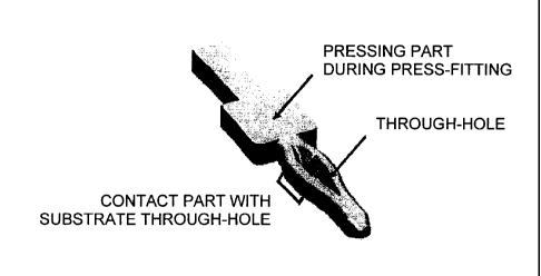
Figure 1 is an illustrative diagram of a press-fit
terminal according to the embodiment. As shown in Figure
2, in a metal material 10 used as a material of the
press-fit terminal, a C layer 12 is formed on the surface
of a base material 11; a B layer 13 is formed on the
surface of the C layer 12; and an A layer 14 is formed on
the surface of the B layer 13.
[0047]
<Constitution of press-fit terminal>
(Base material)
CA 02863505 2014-07-31
- 22 -
The base material 11 is not especially limited, but
usable are metal base materials, for example, copper and
copper alloys, Fe-based materials, stainless steels,
titanium and titanium alloys, and aluminum and aluminum
alloys. The structure and shape or the like of the
press-fit terminal are not especially limited. A general
press-fit terminal includes a plurality of terminals
(multi-pin) arranged in parallel, and is fixed to a
substrate.
[0048]
(A layer)
The A layer needs to be Sn, In, or an alloy thereof.
Sn and In, though being oxidative metals, have a feature
of being relatively soft among metals. Therefore, even
if an oxide film is formed on the Sn and In surface, when
the press-fit terminal is inserted into the substrate,
since the oxide film is easily shaven to thereby make the
contact of metals, a low contact resistance can be
provided.
Sn and In are excellent in the gas corrosion
resistance to gases such as chlorine gas, sulfurous acid
gas, and hydrogen sulfide gas; and for example, in the
case where Ag, inferior in the gas corrosion resistance,
is used for the B layer 13; Ni, inferior in the gas
corrosion resistance, is used for the C layer 12; and
copper and a copper alloy, inferior in the gas corrosion
resistance, are used for the base material 11, Sn and In
CA 02863505 2014-07-31
- 23 -
have a function of improving the gas corrosion resistance
of the press-fit terminal. Here, among Sn and In, Sn is
preferable because In is under a strict regulation based
on the technical guideline regarding the health hazard
prevention of the Ministry of Health, Labor, and Welfare.
[0049]
The composition of the A layer 14 comprises 50 mass%
or more of Sn, In, or the total of Sn and In, and the
other alloy component(s) may be constituted of one or two
or more metals selected from the group consisting of Ag,
As, Au, Bi, Cd, Co, Cr, Cu, Fe, In, Mn, Mo, Ni, Pb, Sb,
Sn, W, and Zn. The composition of the A layer 14 forms
an alloy (for example, the A layer is subjected to Sn-Ag
plating), and thereby, the composition further improves a
whisker resistance, provides a further low inserting
force, is further unlikely to cause shaving of plating
when the press-fit terminal is inserted into the
substrate, and improves a heat resistance in some cases.
[0050]
The thickness of the A layer 14 needs to be 0.002 to
0.2 m. The thickness of the A layer 14 is preferably
0.01 to 0.1 m. With the thickness of the A layer 14 of
smaller than 0.002 m, a sufficient gas corrosion
resistance cannot be provided; and when the press-fit
terminal is subjected to a gas corrosion test using
chlorine gas, sulfurous acid gas, hydrogen sulfide gas,
or the like, the press-fit terminal is corroded to
CA 02863505 2014-07-31
- 24 -
thereby largely increase the contact resistance as
compared with before the gas corrosion test. In order to
provide a more sufficient gas corrosion resistance, the
thickness is preferably 0.01 pm or larger. If the
thickness becomes large, the adhesive wear of Sn and In
becomes much; the inserting force becomes high; and the
plating is liable to be shaven when the press-fit
terminal is inserted into the substrate. In order to
provide a more sufficiently low inserting force and be
further unlikely to cause shaving of plating when the
press-fit terminal is inserted into the substrate, the
thickness is made to be 0.2 pm or smaller. The thickness
is more preferably 0.15 pm or smaller, and still more
preferably 0.10 pm or smaller.
[0051]
The deposition amount of Sn, In of the A layer 14
needs to be 1 to 150 pg/cm2. The deposition amount of
the A layer 14 is preferably 7 to 75 pg/cm2. Here, the
reason to define the deposition amount will be described.
For example, in some cases of measuring the thickness of
the A layer 14 by an X-ray fluorescent film thickness
meter, due to an alloy layer formed between the A layer
and the underneath B layer, an error may be produced in
the value of the measured thickness. By contrast, the
case of the control using the deposition amount can carry
out more exact quality control, not influenced by the
formation situation of the alloy layer. If the
CA 02863505 2014-07-31
- 25 -
deposition amount of Sn, In of the A layer 14 is smaller
than 1 pg/cm2, a sufficient gas corrosion resistance
cannot be provided. If the press-fit terminal is
subjected to a gas corrosion test using chlorine gas,
sulfurous acid gas, hydrogen sulfide gas, or the like,
the press-fit terminal is corroded to thereby largely
increase the contact resistance as compared with before
the gas corrosion test. In order to provide a more
sufficient gas corrosion resistance, the deposition
amount is preferably 7 pg/cm2 or larger. If the
deposition amount becomes large, the adhesive wear of Sn
and In becomes much; the inserting force becomes high;
and the plating is liable to be shaven when the press-fit
terminal is inserted into the substrate. In order to
provide a more sufficiently low inserting force and be
further unlikely to cause shaving of plating when the
press-fit terminal is inserted into the substrate, the
deposition amount is made to be 150 pg/cm2 or smaller.
The deposition amount is more preferably 110 pg/cm2 or
smaller, and still more preferably 75 pg/cm2 or smaller.
[0052]
(B layer)
The B layer 13 needs to be constituted of one or two
or more selected from the group consisting of Ag, Au, Pt,
Pd, Ru, Rh, Os, and Ir. Ag, Au, Pt, Pd, Ru, Rh, Os, and
Ir have a feature of relatively having a heat resistance
among metals. Therefore, the B layer suppresses the
CA 02863505 2014-07-31
- 26 -
diffusion of the compositions of the base material 11 and
the C layer 12 to the A layer 14 side, and improves the
heat resistance. These metals form compounds with Sn and
In of the A layer 14 and suppress the oxide film
formation of Sn and In. Among Ag, Au, Pt, Pd, Ru, Rh, Os,
and Ir, Ag is more desirable from the viewpoint of the
conductivity. Ag has high conductivity. For example, in
the case of using Ag for applications of high-frequency
signals, the skin effect reduces the impedance resistance.
The alloy composition of the B layer 13 comprises 50
mass% or more of Ag, Au, Pt, Pd, Ru, Rh, Os, Ir, or the
total of Ag, Au, Pt, Pd, Ru, Rh, Os, and Ir, and the
other alloy component(s) may be constituted of one or two
or more metals selected from the group consisting of Ag,
Au, Bi, Cd, Co, Cu, Fe, In, Ir, Mn, Mo, Ni, Pb, Pd, Pt,
Rh, Ru, Sb, Se, Sn, W, Tl, and Zn. The composition of
the B layer 13 forms an alloy (for example, the B layer
is subjected to Ag-Sn plating), and thereby, the
composition further improves a whisker resistance,
provides a further low inserting force, is further
unlikely to cause shaving of plating when the press-fit
terminal is inserted into the substrate, and improves a
heat resistance in some cases.
[0053]
The thickness of the B layer 13 needs to be 0.001 to
0.3 m. The thickness of the B layer 13 is preferably
0.005 to 0.1 m. If the thickness is smaller than 0.001
CA 02863505 2014-07-31
- 27 -
gm, the base material 11 or the C layer 12 and the A
layer form an alloy, and the contact resistance after a
heat resistance test becomes worsened. In order to
provide a more sufficient heat resistance, the thickness
is preferably 0.005 gm or larger. If the thickness
becomes large, the inserting force becomes high; and the
plating is liable to be shaven when the press-fit
terminal is inserted into the substrate. In order to
provide a more sufficiently low inserting force and be
further unlikely to cause shaving of plating when the
press-fit terminal is inserted into the substrate, the
thickness is 0.3 gm or smaller, more preferably 0.15 gm
or smaller, and more preferably 0.10 gm or smaller.
[0054]
The deposition amount of Ag, Au, Pt, Pd, Ru, Rh, Os,
Ir, or an alloy thereof of the B layer 13 needs to be 1
to 330 gg/cm2. The deposition amount of the B layer 13
is preferably 4 to 120 gg/cm2. Here, the reason to
define the deposition amount will be described. For
example, in some cases of measuring the thickness of the
B layer 13 by an X-ray fluorescent film thickness meter,
due to an alloy layer formed between the A layer 14 and
the underneath B layer 13, an error may be produced in
the value of the measured thickness. By contrast, the
case of the control using the deposition amount can carry
out more exact quality control, not influenced by the
formation situation of the alloy layer. With the
CA 02863505 2014-07-31
- 28 -
deposition amount of smaller than 1 g/cm2, the base
material 11 or the C layer 12 and the A layer form an
alloy, and the contact resistance after a heat resistance
test becomes worsened. In order to provide a more
sufficient heat resistance, the deposition amount is
preferably 4 pg/cm2 or larger. If the deposition amount
is large, the inserting force becomes high; and the
plating is liable to be shaven when the press-fit
terminal is inserted into the substrate. In order to
provide a more sufficiently low inserting force and be
further unlikely to cause shaving of plating when the
press-fit terminal is inserted into the substrate, the
deposition amount is 330 g/cm2 or smaller, more
preferably 180 g/cm2 or smaller, and still more
preferably 120 g/cm2 or smaller.
[0055]
(C layer)
Between the base material 11 and the B layer 13, the
C layer 12 constituted of one or two or more selected
from the group consisting of Ni, Cr, Mn, Fe, Co, and Cu
needs to be formed. By forming the C layer 12 by using
one or two or more metals selected from the group
consisting of Ni, Cr, Mn, Fe, Co, and Cu, the thin film
lubrication effect is improved due to the formation of
the hard C layer, and thereby a sufficiently low
inserting force can be provided. The C layer 12 prevents
the diffusion of constituting metals of the base material
CA 02863505 2014-07-31
- 29 -
11 to the B layer to thereby improve the durability
including the suppression of the increase in the contact
resistance after the heat resistance test and the gas
corrosion resistance test.
[0056]
The alloy composition of the C layer 12 comprises 50
mass% or more of the total of Ni, Cr, Mn, Fe, Co, and Cu,
and may further comprise one or two or more selected from
the group consisting of B, P, Sn, and Zn. By making the
alloy composition of the C layer 12 to have such a
constitution, the C layer is further hardened to thereby
further improve the thin film lubrication effect to
provide the low inserting force; and the alloying of the
C layer 12 further prevents the diffusion of constituting
metals of the base material 11 to the B layer to thereby
improve the durability including the suppression of the
increase in the contact resistance after the heat
resistance test and the gas corrosion resistance test.
[0057]
The thickness of the C layer 12 needs to be 0.05 m
or larger. With the thickness of the C layer 12 of
smaller than 0.05 m, the thin film lubrication effect by
the hard C layer decreases to thereby provide the high
inserting force; and the constituting metals of the base
material 11 become liable to diffuse to the B layer to
thereby worsen the durability including the increase in
CA 02863505 2014-07-31
- 30 -
the contact resistance after the heat resistance test and
the gas corrosion resistance test.
[0058]
The deposition amount of Ni, Cr, Mn, Fe, Co, Cu of
the C layer 12 needs to be 0.03 mg/cm2 or larger. Here,
the reason to define the deposition amount will be
described. For example, in some cases of measuring the
thickness of the C layer 12 by an X-ray fluorescent film
thickness meter, due to alloy layers formed with the A
layer 14, the B layer 13, the base material 11, or the
like, an error may be produced in the value of the
measured thickness. By contrast, the case of the control
using the deposition amount can carry out more exact
quality control, not influenced by the formation
situation of the alloy layer. With the deposition amount
of smaller than 0.03 mg/cm2, the thin film lubrication
effect by the hard C layer decreases to thereby provide
the high inserting force; and the constituting metals of
the base material 11 become liable to diffuse to the B
layer to thereby worsen the durability including the
increase in the contact resistance after the heat
resistance test and the gas corrosion resistance test.
[0059]
(Heat treatment)
After the A layer 14 is formed, for the purpose of
further improving a whisker resistance, providing a
further low inserting force, being further unlikely to
CA 02863505 2014-07-31
- 31 -
cause shaving of plating when the press-fit terminal is
inserted into the substrate, or improving a heat
resistance, a heat treatment may be carried out. The
heat treatment makes it easy for the A layer 14 and the B
layer 13 to form an alloy layer to thereby improve the
whisker resistance, to be thereby further unlikely to
cause shaving of plating when the press-fit terminal is
inserted into the substrate, to thereby improve the heat
resistance, and to thereby provide further low adhesion
of Sn to provide a low inserting force. Here, the heat
treatment is not limited. However, the heat treatment is
preferably carried out at a temperature of 50 to 500 C
within 12 hours. If the temperature is lower than 50 C,
the A layer 14 and the B layer 13 hardly form the alloy
layer because of the low temperature. If the temperature
is higher than 500 C, the base material 11 or the C layer
12 diffuses to the B layer 13 and the A layer 14 to
thereby provide the high contact resistance in some cases.
If the heat treatment time is longer than 12 hours, the
base material 11 or the C layer 12 diffuses to the B
layer 13 and the A layer 14 to thereby provide the high
contact resistance in some cases.
[0060]
(Post-treatment)
On the A layer 14 or after the heat treatment is
carried out on the A layer 14, for the purpose of
providing a further low inserting force, being further
CA 02863505 2014-07-31
- 32 -
unlikely to cause shaving of plating when the press-fit
terminal is inserted into the substrate, and improving a
heat resistance, a post-treatment may be carried out.
The post-treatment improves the lubricity, to thereby
provide a further low inserting force, makes shaving of
plating unlikely to be caused, and suppresses the
oxidation of the A layer and the B layer, to thereby
improve the durability such as a heat resistance and a
gas corrosion resistance. The post-treatment
specifically includes a phosphate salt treatment, a
lubrication treatment, and a silane coupling treatment,
using inhibitors. Here, the post-treatment is not
limited.
[0061]
<Properties of metal material>
The Vickers hardness as measured from the surface of
the A layer 14 is preferably Hv100 or higher. With the
Vickers hardness as measured from the surface of the A
layer 14 of Hv100 or higher, the hard A layer improves
the thin film lubrication effect and provides the low
inserting force. By contrast, the Vickers hardness as
measured from the surface of the A layer 14 is preferably
Hv1,000 or lower. With the Vickers hardness as measured
from the surface of the A layer 14 of Hv1,000 or lower,
the bending workability is improved; and in the case
where the press-fit terminal according to the present
invention is press-formed, cracks are hardly generated in
CA 02863505 2014-07-31
- 33 -
the formed portion, and the decrease in the gas corrosion
resistance is suppressed.
The indentation hardness as measured from the
surface of the A layer 14 is preferably 1,000 MPa or
higher. Here, the indentation hardness as measured from
the surface of the A layer 14 is a hardness acquired by
measuring an impression made on the surface of the A
layer by a load of 0.1 mN in an ultrafine hardness test.
With the surface indentation hardness of the A layer 14
of 1,000 MPa or higher, the hard A layer improves the
thin film lubrication effect and provides a low inserting
force. By contrast, the Vickers indentation hardness as
measured from the surface of the A layer 14 is preferably
10,000 MPa or lower. With the surface indentation
hardness of the A layer 14 of 10,000 MPa or lower, the
bending workability is improved; and in the case where
the press-fit terminal according to the present invention
is press-formed, cracks are hardly generated in the
formed portion, and the decrease in the gas corrosion
resistance is suppressed.
[0062]
The arithmetic average height (Ra) of the surface of
the A layer 14 is preferably 0.1 gm or lower. With the
arithmetic average height (Ra) of the surface of the A
layer 14 of 0.1 gm or lower, since convex portions, which
are relatively easily corroded, become few and the
CA 02863505 2014-07-31
- 34 -
surface becomes smooth, the gas corrosion resistance is
improved.
The maximum height (Rz) of the surface of the A
layer 14 is preferably 1 gm or lower. With the maximum
height (Rz) of the surface of the A layer 14 of 1 pla or
lower, since convex portions, which are relatively easily
corroded, become few and the surface becomes smooth, the
gas corrosion resistance is improved.
The surface reflection density of the A layer 14 is
preferably 0.3 or higher. With the surface reflection
density of the A layer 14 of 0.3 or higher, since convex
portions, which are relatively easily corroded, become
few and the surface becomes smooth, the gas corrosion
resistance is improved.
[0063]
The cross-section Vickers hardness of the C layer 12
is preferably Hv300 or higher. With the cross-section
Vickers hardness of the C layer 12 of Hv300 or higher,
the C layer is further hardened to thereby further
improve the thin film lubrication effect to provide a low
inserting force. By contrast, the cross-section Vickers
hardness of the C layer 12 is preferably Hv1,000 or lower.
With the cross-section Vickers hardness of the C layer 12
of Hv1,000 or lower, the bending workability is improved;
and in the case where the press-fit terminal according to
the present invention is press-formed, cracks are hardly
CA 02863505 2014-07-31
- 35 -
generated in the formed portion, and the decrease in the
gas corrosion resistance is suppressed.
[0064]
The cross-section Vickers hardness of the C layer 12
and the thickness of the C layer 12 preferably satisfy
the following expression:
Vickers hardness (Hv) -376.22Ln
(thickness: pm) +
86.411.
If the cross-section Vickers hardness of the C layer 12
and the thickness of the C layer 12 satisfy the above
expression, the C layer is further hardened to thereby
further improve the thin film lubrication effect to
provide the low inserting force.
Here, in the present invention, "Ln (thickness: pm)"
refers to a numerical value of a natural logarithm of a
thickness (pm).
[0065]
The cross-section indentation hardness of the C
layer 12 is preferably 2,500 MPa or higher. Here, the
cross-section indentation hardness of the C layer 12 is a
hardness acquired by measuring an impression made on the
cross-section of the C layer 12 by a load of 0.1 mN in an
ultrafine hardness test. With the cross-section
indentation hardness of the C layer 12 of 2,500 MPa or
higher, the C layer is further hardened to thereby
further improve the thin film lubrication effect to
provide the low inserting force. By contrast, the cross-
CA 02863505 2014-07-31
- 36 -
section indentation hardness of the C layer 12 is
preferably 10,000 MPa or lower. With the cross-section
indentation hardness of the C layer 12 of 10,000 MPa or
lower, the bending workability is improved; and in the
case where the press-fit terminal according to the
present invention is press-formed, cracks are hardly
generated in the formed portion, and the decrease in the
gas corrosion resistance is suppressed.
[0066]
The cross-section indentation hardness of the C
layer 12 and the thickness of the C layer 12 preferably
satisfy the following expression:
Indentation hardness (MPa) -3998.4Ln (thickness:
m) + 1178.9.
If the cross-section indentation hardness of the C layer
12 and the thickness of the C layer 12 satisfy the above
expression, the C layer is further hardened to thereby
further improve the thin film lubrication effect to
provide the low inserting force.
[0067]
When a depth analysis by XPS (X-ray photoelectron
spectroscopy) is carried out, it is preferable that a
position (Di) where the atomic concentration (at%) of Sn
or In of the A layer 14 is a maximum value, a position
(D2) where the atomic concentration (at%) of Ag, Au, Pt,
Pd, Ru, Rh, Os, or Ir of the B layer 13 is a maximum
value, and a position (Dfl where the atomic concentration
CA 02863505 2014-07-31
- 37 -
(at%) of Ni, Cr, Mn, Fe, Co, or Cu of the C layer 12 is a
maximum value are present in the order of Di, D2, and D3
from the outermost surface. If the positions are not
present in the order of Di, D2, and D3 from the outermost
surface, there arises a risk that: a sufficient gas
corrosion resistance cannot be provided; and when the
press-fit terminal is subjected to a gas corrosion test
using chlorine gas, sulfurous acid gas, hydrogen sulfide
gas, or the like, the press-fit terminal is corroded to
thereby largely increase the contact resistance as
compared with before the gas corrosion test.
When a depth analysis by XPS (X-ray photoelectron
spectroscopy) is carried out, it is preferable that: the
A layer 14 has a maximum value of an atomic concentration
(at%) of Sn or In of 10 at% or higher, and the B layer 13
has a maximum value of an atomic concentration (at%) of
Ag, Au, Pt, Pd, Ru, Rh, Os, or Ir of 10 at% or higher;
and a depth where the atomic concentration (at%) of Ni,
Cr, Mn, Fe, Co, or Cu of the C layer 12 is 25 at% or
higher is 50 nm or more. In the case where the maximum
value of the atomic concentration (at%) of Sn or In of
the A layer 14, and the maximum value of the atomic
concentration (at%) of Ag, Au, Pt, Pd, Ru, Rh, Os, or Ir
of the B layer 13 are each lower than 10 at%; and where a
depth where the atomic concentration (at%) of Ni, Cr, Mn,
Fe, Co, or Cu of the C layer 12 is 25 at% or higher is
shallower than 50 nm, there arises a risk that the
CA 02863505 2014-07-31
- 38 -
inserting force is high, and the base material components
diffuse to the A layer 14 or the B layer 13 to thereby
worsen the heat resistance and the gas corrosion
resistance.
When a depth analysis by XPS (X-ray photoelectron
spectroscopy) is carried out, it is preferable that
between a position ( i) where the atomic concentration
(at%) of Sn or In of the A layer 14 is a maximum value
and a position (Dfl where the atomic concentration (at%)
of Ni, Cr, Mn, Fe, Co, Cu, or Zn of the C layer 12 is a
maximum value, a region having 40 at% or more of Ag, Au,
Pt, Pd, Ru, Rh, Os, or Ir is present in a thickness of 1
nm or larger. If the region is present in a thickness of
smaller than 1 nm, for example, in the case of Ag, there
arises a risk of worsening the heat resistance.
When an elemental analysis of the surface of the A
layer is carried out by a survey measurement by XPS (X-
ray photoelectron spectroscopy), it is preferable that
the content of Sn, In is 2 at% or higher. If the content
of Sn, In is lower than 2 at%, for example, in the case
of Ag, there arises a risk that the sulfurization
resistance is inferior and the contact resistance largely
increases. For example, in the case of Pd, there arises
a risk that Pd is oxidized to thereby raise the contact
resistance.
When an elemental analysis of the surface of the A
layer is carried out by a survey measurement by XPS (X-
CA 02863505 2014-07-31
- 39 -
ray photoelectron spectroscopy), it is preferable that
the content of Ag, Au, Pt, Pd, Ru, Rh, Os, or Ir is lower
than 7 at%. If the content of Ag, Au, Pt, Pd, Ru, Rh, Os,
or Ir is 7 at% or higher, for example, in the case of Ag,
there arises a risk that the sulfurization resistance is
inferior and the contact resistance largely increases.
For example, in the case of Pd, there arises a risk that
Pd is oxidized to thereby raise the contact resistance.
When an elemental analysis of the surface of the A
layer is carried out by a survey measurement by XPS (X-
ray photoelectron spectroscopy), it is preferable that
the content of 0 is lower than 50 at%. If the content of
0 is 50 at% or higher, there arises a risk of raising the
contact resistance.
[0068]
<Method for manufacturing a press-fit terminal>
A method for manufacturing the press-fit terminal
according to the present invention is not limited. The
press-fit terminal can be manufactured by subjecting a
base material previously formed into a press-fit terminal
shape by press-forming or the like to wet (electro-,
electroless) plating, dry (sputtering, ion plating, or
the like) plating, or the like.
[Examples]
[0069]
Hereinafter, although Examples of the present
invention will be described with Comparative Examples,
CA 02863505 2014-07-31
- 40 -
these are provided to better understand the present
invention, and are not intended to limit the present
invention.
[0070]
As Examples and Comparative Examples, samples to be
formed by providing a base material, a C layer, a B layer,
and an A layer in this order, and possibly heat-treating
the resultant, were each fabricated under the conditions
shown in the following Tables 1 to 7.
Specifications of press-fit terminals and through-
holes are shown in Table 1; the fabrication condition of
C layers is shown in Table 2; the fabrication condition
of B layers is shown in Table 3; the fabrication
condition of A layers is shown in Table 4; and the heat
treatment condition is shown in Table 5. The fabrication
conditions and the heat treatment conditions of the each
layer used in each Example are shown in Table 6; and the
fabrication conditions and the heat treatment conditions
of the each layer used in each Comparative Example are
shown in Table 7.
[0071]
[Table 1]
Specification of Press-Fit Specification of Through-Hole
Terminal
made by Tokiwa & Co., Inc., Thickness of substrate: 2 mm
Press-fit terminal PCB through-hole: (I) 1 mm
connector, R800
[0072]
CA 02863505 2014-07-31
- 41 -
[Table 2]
Condition of Underlayers (C Layers)
No. Surface Treatment Detail
Method
1 Electroplating Plating liquid: Ni sulfamate plating liquid
Plating temperature: 55 C
Current density: 0.5 to 4 A/dm2
2 Electroplating Plating liquid: Cu sulfate plating liquid
Plating temperature: 30 C
Current density: 2.3 A/dm2
3 Electroplating Plating liquid: chromium sulfate liquid
Plating temperature: 30 C
Current density: 4 A/dm2
4 Sputtering Target: having a predetermined composition
Apparatus: sputtering apparatus made by Ulvac, Inc.
Output: DC 50 W
Argon pressure: 0.2 Pa
Electroplating Plating liquid: Fe sulfate liquid
Plating temperature: 30 C
Current density: 4 A/dm2
6 Electroplating Plating liquid: Co sulfate bath
Plating temperature: 30 C
Current density: 4 A/dm2
7 Electroplating Plating liquid: Ni sulfamate plating liquid +
saccharin
Plating temperature: 55 C
Current density: 4 A/dm2
8 Electroplating Plating liquid: Ni sulfamate plating liquid +
saccharin +
additive
Plating temperature: 55 C
Current density: 4 A/dm2
[0073]
CA 02863505 2014-07-31
¨ 42 ¨
[Table 3]
Condition of Middle Layers (B Layers)
No. Surface Treatment Detail
Method
1 Electroplating Plating liquid: Ag cyanide plating liquid
Plating temperature: 40 C
Current density: 0.2 to 4 AJdm2
2 Electroplating Plating liquid: Au cyanide plating liquid
Plating temperature: 40 C
Current density: 0.2 to 4 A/dm2
3 Electroplating Plating liquid: chloroplatinic acid plating liquid
Plating temperature: 40 C
Current density: 0.2 to 4 A/dm2
4 Electroplating Plating liquid: diammine palladium (II) chloride
plating
liquid
Plating temperature: 40 C
Current density: 0.2 to 4 A/dm2
Electroplating Plating liquid: Ru sulfate plating liquid
Plating temperature: 40 C
Current density: 0.2 to 4 A/dm2
6 Sputtering Target: having a predetermined composition
Apparatus: sputtering apparatus made by Ulvac, Inc.
Output: DC 50 W
Argon pressure: 0.2 Pa
7 Electroplating Plating liquid: Sn methanesulfonate plating liquid
Plating temperature: 40 C
Current density: 0.2 to 4 AJdm2
8 Electroplating Plating liquid: Cu sulfate plating liquid
Plating temperature: 30 C
Current density: 2.3 A/dm2
[0074]
CA 02863505 2014-07-31
- 43 -
[Table 4]
Condition of Base Material of Outermost Surface Layers (A Layers)
No. Surface Treatment Detail
Method
1 Electroplating Plating liquid: Sn methanesulfonate plating liquid
Plating temperature: 40 C
Current density: 0.2 to 4 A/dm2
2 Sputtering Target: having a predetermined composition
Apparatus: sputtering apparatus made by Ulvac, Inc.
Output: DC 50 W
Argon pressure: 0.2 Pa
3 Electroplating Plating liquid: Ag cyanide plating liquid
Plating temperature: 40 C
Current density: 0.2 to 4 A/dm2
[0075]
[Table 5]
Heat Treatment Condition
No. Temperature [ C] Time [second]
1 300 5
2 300 20
3 30 12 hours
4 50 12 hours
50 20 hours
6 300 3
7 500 1
8 600 1
[0076]
CA 02863505 2014-07-31
- 44 -
[Table 6-1]
Example No. Outermost Surface Middle Layer Underlayer (C Heat
Layer (A Layer) (B Layer) Layer) Treatment
Condition No. Condition No. Condition No. Condition No.
see Table 4 see Table 3 see Table 2 see Table 5
1 1 1 1 ---
2 1 1 1 ---
3 1 1 1 ---
4 1 1 1 ---
1 1 1 ---
6 2 1 1 ---
7 2 1 1 ---
8 2 1 1 ---
9 2 1 1 ---
2 1 1 ---
11 2 1 1 ---
12 2 1 1 ---
13 2 1 1 ---
14 2 1 1 ---
2 1 1 ---
16 2 1 1 ---
17 2 1 1 ---
18 2 1 1 ---
19 2 1 1 ---
2 1 1 ---
21 2 1 1 ---
22 2 1 1 ---
23 2 1 1 ---
24 1 2 1 ---
1 3 1 ---
26 1 4 1 ---
27 1 5 1 ---
28 1 6 1 ---
29 1 6 1 ---
1 6 1 ---
[0077]
CA 02863505 2014-07-31
¨ 45 ¨
[Table 6-2]
Example No. Outermost Surface Middle Layer Underlayer (C Heat
Treatment
Layer (A Layer) (B Layer) Layer) Condition No.
Condition No. Condition No. Condition No. see Table 5
see Table 4 see Table 3 see Table 2
31 1 6 1 - - -
32
33 1 6 1 - - -
34 1 6 1 - - -
35 1 6 1 - - -
36 1 6 1 - - -
37 1 6 1 - - -
38 1 6 1 - - -
39 1 6 1 - - -
40 1 6 1 - - -
41 1 6 1 - - -
42 1 6 1 - - -
43 1 6 1 - - -
44 1 6 1 - - -
45 1 6 1 - - -
46 1 6 1 - - -
47 1 6 1 - - -
48 1 6 1 - - -
49 1 6 1 - - -
50 1 6 1 - - -
51 1 6 1 - - -
52 1 6 1 - - -
53 1 1 3 - - -
54 1 1 4 - - -
55 1 1 5 - - -
56 1 1 6 - - -
57 1 1 2 - - -
58 1 1 4 - - -
59 1 1 4 - - -
60 1 1 4 - - -
61 1 1 4 - - -
62 1 1 4 - - -
63 1 1 4 - - -
64 1 1 4 - - -
65 1 1 4 - - -
66 1 1 4 - - -
67 1 1 1 - - -
68 1 1 7 - - -
69 1 1 8 - - -
70 1 1 1 - - -
[0078]
CA 02863505 2014-07-31
¨ 46 ¨
[Table 6-3]
Example No. Outermost Surface Middle Layer Underlayer (C Heat
Layer (A Layer) (B Layer) Layer) Treatment
Condition No. Condition No. Condition No. Condition No.
see Table 4 see Table 3 see Table 2 see
Table 5
71 1 1 1 ---
72 1 1 1 ---
73 1 1 1 ---
74 1 1 1 ---
75 1 1 1 ---
76 1 1 1 ---
77 1 1 1 ---
78 1 1 1 ---
79 1 1 1 ---
80 1 1 1 ---
81 1 1 7 ---
82 1 1 8 ---
83 1 1 7 ---
84 1 1 7 ---
85 1 1 8 ---
86 1 1 8 ---
87 1 1 4 ---
88 1 1 4 ---
89 1 1 1 1
90 1 1 1 2
91 1 2 1 ---
92 1 2 1 ---
93
94 2 1 1 ---
95 1 1 1 ---
96 1 1 1 3
97 1 1 1 4
98 1 1 1 5
99 1 1 1 6
100 1 1 1 7
101 1 1 1 8
[ 0 0 7 9 ]
CA 02863505 2014-07-31
- 47 -
[Table 7]
Comparative Outermost Surface Middle Layer
Underlayer (C Heat Treatment
Example No. Layer (A Layer) (B Layer) Layer)
Condition No.
Condition No. Condition No. Condition No. see Table 5
see Table 4 see Table 3 see Table 2
1 1 ___ 1 1
2 1 --- 1 1
3 1 --- 1 ---
4 I 8 1 1
1 8 1 1
6 1 8 1 ---
7 1 --- 2 1
8 1 --- 1 1
9 1 1 1 ---
1 1 1 ---
11 1 1 1 ---
12 1 --- I ---
13 1 1 1 ---
14 1 --- 1 ---
1 1 1 ---
16 1 1 1 ---
17 3 7 1 ---
18 1 1 I ---
19 1 --- 1 ---
[0080]
(Measurement of a thickness)
The thicknesses of an A layer, a B layer, and a C
layer were measured by carrying out the each surface
treatment on a base material, and measuring respective
actual thicknesses by an X-ray fluorescent film thickness
meter (made by Seiko Instruments Inc., SEA5100,
collimator: 0.1 mrnd) ) .
[0081]
(Measurement of a deposition amount)
Each sample was acidolyzed with sulfuric acid,
nitric acid, or the like, and measured for a deposition
amount of each metal by ICP (inductively coupled plasma)
CA 02863505 2014-07-31
- 48 -
atomic emission spectroscopy. The acid to be
specifically used depends on the composition of the each
sample.
[0082]
(Determination of a composition)
The composition of each metal was calculated based
on the measured deposition amount.
[0083]
(Determination of a layer structure)
The layer structure of the obtained sample was
determined by a depth profile by XPS (X-ray photoelectron
spectroscopy) analysis. The analyzed elements are
compositions of an A layer, a B layer, and a C layer, and
C and O. These elements are made as designated elements.
With the total of the designated elements being taken to
be 100%, the concentration (at%) of the each element was
analyzed. The thickness by the XPS (X-ray photoelectron
spectroscopy) analysis corresponds to a distance (in
terms of Si02) on the abscissa of the chart by the
analysis.
The surface of the obtained sample was also
subjected to a qualitative analysis by a survey
measurement by XPS (X-ray photoelectron spectroscopy)
analysis. The resolution of the concentration by the
qualitative analysis was set at 0.1 at%.
An XPS apparatus to be used was 5600MC, made by
Ulvac-Phi, Inc., and the measurement was carried out
CA 02863505 2014-07-31
- 49 -
under the conditions of ultimate vacuum: 5.7 x 10⁻⁹ Torr,
exciting source: monochromated AlKa, output: 210 W,
detection area: 800 m(1), incident angle: 45 , takeoff
angle: 45 , and no neutralizing gun, and under the
following sputtering condition.
Ion species: Ar+
Acceleration voltage: 3 kV
Sweep region: 3 mm x 3 mm
Rate: 2.8 nm/min (in terms of Si02)
[0084]
(Evaluations)
Each sample was evaluated for the following items.
A. Inserting force
The inserting force was evaluated by measuring an
inserting force when a press-fit terminal was inserted
into a substrate. A measurement apparatus used in the
test was 1311NR, made by Aikoh Engineering Co., Ltd. The
press-fit terminal was slid for the test in a state where
the substrate was fixed. The number of the samples was
set to be five; and a value obtained by averaging the
values of the maximum inserting forces of the samples was
employed as the inserting force. Samples of Comparative
Example 1 were employed as a blank material for the
inserting force.
The target of the inserting force was lower than 85%
of the maximum inserting force of Comparative Example 1.
Because Comparative Example 4 having an inserting force
CA 02863505 2014-07-31
- 50 -
of 90% of the maximum inserting force of Comparative
Example 1 was present as an actual product, the inserting
force lower than 85% of the maximum inserting force of
Comparative Example 1 and lower than that in Comparative
Example 4 by 5% or more was targeted.
[0085]
B. Whisker
The press-fit terminal was inserted into the
through-hole of the substrate by a hand press, and a
thermal shock cycle test (JETTA ET-7410) was carried out.
The sample whose test had been finished was observed at a
magnification of 100 to 10,000 times by a SEM (made by
JEOL Ltd., type: JSM-5410) to observe the generation
situation of whiskers.
Thermal shock cycle test>
Low temperature -40 C x 30 minutes 4-> high
temperature 85 C x 30 minutes/cycle x 1000 cycles
The target property was that no whiskers of 20 m or
longer in length were generated, but the top target was
that no whisker at all was generated.
[0086]
C. Contact resistance
The contact resistance was measured using a contact
simulator CRS-113-Au, made by Yamasaki-Seiki Co., Ltd.,
by a four-terminal method under the condition of a
contact load of 50 g. The number of the samples was made
to be five, and a range of from the minimum value to the
CA 02863505 2014-07-31
- 51 -
maximum value of the samples was employed. The target
property was a contact resistance of 10 mfl or lower. The
contact resistance was classified into 1 to 3 mi-2, 3 to 5
mO, and higher than 5 mil.
[0087]
D. Heat resistance
The heat resistance was evaluated by measuring the
contact resistance of a sample after an atmospheric
heating (175 C x 500 h) test. The target property was a
contact resistance of 10 mf2 or lower, but the top target
was made to be no variation (being equal) in the contact
resistance before and after the heat resistance test.
The heat resistance was classified into 1 to 4 mD, 2 to
4 m.Q, 2 to 5 mQ, 3 to 6 m12, 3 to 7 mO, 6 to 9 mn, and
higher than 10 mi) in terms of contact resistance.
[0088]
E. Gas corrosion resistance
The gas corrosion resistance was evaluated by three
test environments shown in (1) to (3) described below.
The evaluation of the gas corrosion resistance was
carried out by using the contact resistance of a sample
after the environment tests of (1) to (3). The target
property was a contact resistance of 10 mC2 or lower, but
the top target was made to be no variation (being equal)
in the contact resistance before and after the gas
corrosion resistance test. The gas corrosion resistance
was classified into 1 to 3 mi-2, 1 to 4 mn, 2 to 4 mn, 2
CA 02863505 2014-07-31
- 52 -
to 6 an, 3 to 5 riLQ, 3 to 7 ni0, 4 to 7 IrD, 5 to 8 rrn, 6
to 9 n1.0, and higher than 10 mn in terms of contact
resistance.
(1) Salt spray test
Salt concentration: 5%
Temperature: 35 C
Spray pressure: 98 10 kPa
Exposure time: 96 h
(2) Sulfurous acid gas corrosion test
Sulfurous acid concentration: 25 ppm
Temperature: 40 C
Humidity: 80% RH
Exposure time: 96 h
(3) Hydrogen sulfide gas corrosion test
Sulfurous acid concentration: 10 ppm
Temperature: 40 C
Humidity: 80% RH
Exposure time: 96 h
[0089]
G. Bending workability
The bending workability was evaluated by a 90
bending of a sample under the condition that the ratio of
the thickness and the bending radius of the sample became
1 by using a letter-W-shape die. The evaluation was made
as good in the case where no crack was observed in the
observation of the surface of the bending-worked portion
by an optical microscope, posing no practical problem;
CA 02863505 2014-07-31
- 53 -
and as poor in the case where any cracks were observed
therein.
[0090]
H. Vickers hardness
The Vickers hardnesses of an A layer and a C layer
were measured by making an impression by a load of 980.7
mN (Hv0.1) from the surface of the A layer and the cross-
section of the C layer in a load retention time of 15 sec.
[0091]
I. Indentation hardness
The indentation hardnesses of an A layer and a C
layer were measured by making an impression on the
surface of the A layer and the cross-section of the C
layer at a load of 0.1 mN by an ultrafine hardness tester
(ENT-2100, made by Elionix Inc.).
[0092]
J. Surface roughness
The surface roughnesses (arithmetic average height
(Ra) and maximum height (Rz)) were measured according to
JIS B 0601 by using a non-contact type three dimensional
measurement instrument (made by Mitaka Kohki Co., Ltd.,
type: NH-3). The measurement was carried out five times
per sample, with a cutoff of 0.25 mm and a measurement
length of 1.50 mm.
[0093]
K. Reflection density
CA 02863505 2014-07-31
- 54 -
The reflection density was measured using a
densitometer (ND-1, made by Nippon Denshoku Industries
Co., Ltd.).
[0094]
L. Generation of powder
The press-fit terminal inserted into the through-
hole was extracted from the through-hole, and the cross-
section of the press-fit terminal was observed at a
magnification of 100 to 10,000 times by a SEM (made by
JEOL Ltd., type: JSM-5410) to observe the generation
status of powder. The press-fit terminal with which the
diameter of the powder was smaller than 5 m was made as
good; the press-fit terminal with which the diameter of
the powder was 5 to smaller than 10 m was made as
average; and the press-fit terminal with which the
diameter of the powder was 10 m or larger was made as
poor.
The respective conditions and evaluation results are
shown in Tables 8 to 22.
[0095]
CA 02863505 2014-07-31
- 55 -
[Table 8]
Heat
A Layer B Layer C Layer Treatme
nt
Thickne
Depositio Depositio Depositio
ss ss ss
Compositi n Compositi Thickne n Compositi Thickne
n Conditio
on Amount on Amount on Amount n
ilmli blecm21 [I-tmi [I-Lecm2i [pm] [mg/cm2]
1 Sn 0.2 146 Ag 0.3 315 Ni 1.0 0.9 None
2 Sn 0.2 146 Ag 0.001 1 Ni 1.0 0.9 None
3 Sn 0.03 22 Ag 0.03 32 Ni 1.0 0.9 None
4 Sn 0.002 1 Ag 0.3 315 Ni 1.0 0.9 None
Sn 0.002 1 Ag 0.001 1 Ni 1.0 0.9 None
6 In 0.03 22 Ag 0.03 32 Ni 1.0 0.9 None
7 Sn-2Ag 0.03 22 Ag 0.03 32 Ni 1.0 0.9 None
8 Sn-2As 0.03 22 Ag 0.03 32 Ni 1.0 0.9 None
9 Sn-2Au 0.03 22 Ag 0.03 32 Ni 1.0 0.9 None
1
Sn-2Bi 0.03 22 Ag 0.03 32 Ni 1.0 0.9 None
0
1
Sn-2Cd 0.03 22 Ag 0.03 32 Ni 1.0 0.9 None
1
1
Sn-2Co 0.03 22 Ag 0.03 32 Ni 1.0 0.9 None
2
1
Sn-2Cr 0.03 22 Ag 0.03 32 Ni 1.0 0.9 None
3
1
Sn-2Cu 0.03 22 Ag 0.03 32 Ni 1.0 0.9 None
4
1
Sn-2Fe 0.03 22 Ag 0.03 32 Ni 1.0 0.9 None
5
1
Sn-2In 0.03 22 Ag 0.03 32 Ni 1.0 0.9 None
6
1
Sn-2Mn 0.03 22 Ag 0.03 32 Ni 1.0 0.9 None
a.) 7
CI. 1
Sn-2Mo i 0.03 22 Ag 0.03 32 =Ni 1.0 0.9 None 8 .
1
Sn-2Ni 0.03 22 Ag 0.03 32 Ni 1.0 0.9 None
9
2
Sn-2Pb 0.03 22 Ag 0.03 32 Ni 1.0 0.9 None
0
2
Sn-25b 0.03 22 Ag 0.03 32 Ni 1.0 0.9 None
1
2
Sn-2W 0.03 22 Ag 0.03 32 Ni 1.0 0.9 None
2
2
Sn-2Zn 0.03 22 Ag 0.03 32 Ni 1.0 0.9 None
3
2
Sn 0.03 22 Au 0.03 32 Ni 1.0 0.9 None
4
2
Sn 0.03 22 Pt 0.03 32 Ni 1.0 0.9 None
5
2
Sn 0.03 22 Pd 0.03 32 Ni 1.0 0.9 None
6
2
Sn 0.03 22 Ru 0.03 32 Ni 1.0 0.9 None
7
2
Sn 0.03 22 Rh 0.03 32 Ni 1.0 0.9 None
8 .
2
Sn 0.03 22 Os 0.03 32 Ni 1.0 0.9 None
9
3
Sn 0.03 22 Ir 0.03 32 Ni 1.0 0.9 None
0
3 Sn 0.03 22 Ag-2Au 0.03 32 Ni 1.0 0.9 None
CA 02863505 2014-07-31
- 56 -
1
3
Sn 0.03 22 Ag-2Bi 0.03 32 Ni 1.0 0.9
None
2
3
Sn 0.03 22 Ag-2Cd 0.03 32 Ni 1.0 0.9 None
3
3
Sn 0.03 22 Ag-2Co 0.03 32 Ni 1.0 0.9 None
4
3
Sn 0.03 22 Ag-2Cu 0.03 32 Ni 1.0 0.9 None
3
Sn 0.03 22 Ag-2Fe 0.03 32 Ni 1.0 0.9
None
6
3
Sn 0.03 22 Ag-21n 0.03 32 Ni 1.0 0.9
None
7
3
Sn 0.03 22 Ag-21r 0.03 32 Ni 1.0 0.9
None
8
3
Sn 0.03 22 Ag-2Mn 0.03 32 Ni 1.0 0.9 None
9
Targe 0.002 15_ 0.0015_ 15_
0.005_ 0.03
t 5_0.2 150 0.3 330
[0096]
CA 02863505 2014-07-31
- 57 -
[Table 9]
A Layer B Layer C Layer Heat Treatment
z a
o - a z c ..., a z a Condition
=-' :-= S o L .2. g .2 E .9. C'
-15 :g :- = =c-A ,7 0
6 0 g'
a. 5 rA
0,.0
c-) E .7 .--
p.. E 0 1-..)
-
.- u <
C E
:=
E- a) < O. ..=
C
C...) C...) C..)
[gm] [Fte/CM2] himl [g/cm2] [pin] [mg/cm]
40 Sn 0.03 22 Ag-2Mo 0.03 32 Ni 1.0 0.9 None
41 Sn 0.03 22 Ag-2Ni 0.03 32 Ni 1.0 0.9 None
42 Sn 0.03 22 Ag-2Pb 0.03 32 Ni 1.0 0.9
None
43 Sn 0.03 22 Ag-2Pd 0.03 32 Ni 1.0 0.9
None
44 Sn 0.03 22 Ag-2Pt 0.03 32 Ni 1.0 0.9 None
.i.g. 45 Sn 0.03 22 Ag-2Rh 0.03 32 Ni 1.0 0.9 None
46 Sn 0.03 22 Ag-2Ru 0.03 32 Ni 1.0 0.9 None
47 Sn 0.03 22 Ag-2Sb 0.03 32 Ni 1.0 0.9
None
48 Sn 0.03 22 Ag-2Se 0.03 32 Ni 1.0 0.9 None
49 Sn 0.03 22 Ag-2Sn 0.03 32 Ni 1.0 0.9
None
50 Sn 0.03 22 Ag-2W 0.03 32 Ni 1.0 0.9 None
51 Sn 0.03 22 Ag-2T1 0.03 32 Ni 1.0 0.9 None
52 Sn 0.03 22 Ag-2Zn 0.03 32 Ni 1.0 0.9
None
1 Sn 1.0 728 Ni 0.5 0.4 300 C x 5 sec.
2 Sn 0.6 437 Ni 0.5 0.4 300 C x 5 sec.
3 Sn 0.6 437 Ni 0.5 0.4
4 Sn 0.6 437 Cu 0.3 Ni 0.5 0.4 300 C x 5 sec.
5 Sn 0.4 291 Cu 0.3 Ni 0.5 0.4 300 C
x 5 sec.
1)
0. 6 Sn 0.4 291 Cu 0.3 Ni 0.5 0.4
E
mt 7 Sn 1.0 728 Cu 0.5 0.4 300 C x
5 sec.
x
=LI 8 Sn 1.0 728 ___-ÑI 1.0 0.9
300 C x 5 sec.
I.)
a' 9 Sn 0.3 218 Ag 0.3 315 Ni 1.0 0.9 None
Vz
10 Sn 0.3 218 Ag 0.001 1.1 Ni 1.0 0.9 None
a 11 , Sn 0.2 146 Ag 0.5 525 Ni 1.0 0.9 None
u 12 Sn 0.2 146 Ag .../1_,....------ Ni 1.0
0.9 None
13 Sn 0.002 1.5 Ag 0.5 525 Ni 1.0 0.9 None
14 Sn 0.002 1.5 Ag ...õ..-----1,------- Ni
1.0 0.9 None
15 Sn 0.001 0.7 Ag 0.3 315 Ni 1.0 0.9 None
16 Sn 0.001 0.7 Ag 0.001 1.1 Ni 1.0 0.9 None
17 Ag 0.03 32 Sn 0.03 22 Ni 1.0 0.9
None
Target 0.002_ 1_. 0.001 1. 0.005 0.03
__0.2 150 if;1.3 330
[0097]
CA 02863505 2014-07-31
- 58 -
[Table 10]
Heat
Whisker Inserting Force Gas Corrosion Resistance
Resistance
Number Sulfurous Hydrogen
NumberSalt Spray
of Maximum Acid Gas Sulfide
of
Whiskers Whiskers Inserting Contact
Generation
of Force/Maximum Resistance Contact Situation
of 20 gm
Shorter Inserting Force Resistance
Contact Contact Contact of Powder
Than 20 or
of Comparative Resistance Resistance Resistance
Longer in
gm in Length Example 1
Length
[Number] [Number] [ /0] [inf2] [m2] [mc2] [m(2] [m_Q]
1 0 0 82 1-3 1-4 1-4 1-4 1-4 Average
2 0 0 79 1-3 6-9 1-4 1-4 1-4 Average
3 0 0 77 1-3 1-4 1-4 1-4 1-4 Good
4 0 0 79 1-3 1-4 4-7 5-8 6-9 Average
0 0 76 1-3 6-9 4-7 5-8 6-9 Good
6 0 0 77 1-3 1-4 1-4 1-4 1-4 Good
7 0 0 77 1-3 1-4 1-4 1-4 1-4 Good
8 0 0 77 1-3 1-4 1-4 1-4 1-4 Good
9 0 0 77 1-3 1-4 1-4 1-4 1-4 Good
0 0 77 1-3 1-4 1-4 1-4 1-4 Good
11 0 0 77 1-3 1-4 1-4 1-4 1-4 Good
12 0 0 77 1-3 1-4 1-4 1-4 1-4 Good
13 0 0 77 1-3 1-4 1-4 1-4 1-4 Good
14 0 0 77 1-3 1-4 1-4 1-4 1-4 Good
0 0 77 1-3 1-4 1-4 1-4 1-4 Good
16 0 0 77 1-3 1-4 1-4 1-4 1-4 Good
17 0 0 77 1-3 1-4 1-4 1-4 1-4 Good
18 0 0 77 1-3 1-4 1-4 1-4 1-4 Good
.,, 19 0 0 77 1-3 1-4 1-4 1-4 1-4 Good
g 20 0 0 77 1-3 1-4 1-4 1-4 1-4 Good
LI 21 0 0 77 1-3 1-4 1-4 1-4 1-4 Good
22 0 0 77 1-3 1-4 1-4 1-4 1-4 Good
23 0 0 77 1-3 1-4 1-4 1-4 1-4 Good
24 0 0 77 1-3 1-4 1-4 1-4 1-4 Good
0 0 77 1-3 1-4 1-4 1-4 1-4 Good
26 0 0 77 1-3 1-4 1-4 1-4 1-4 Good
27 0 0 77 1-3 1-4 1-4 1-4 1-4 Good
28 0 0 77 1-3 1-4 1-4 1-4 1-4 Good
29 0 0 77 1-3 1-4 1-4 1-4 1-4 Good
0 0 77 1-3 1-4 1-4 1-4 1-4 Good
31 0 0 77 1-3 1-4 1-4 1-4 1-4 Good
32 0 0 77 1-3 1-4 1-4 1-4 1-4 Good
33 0 0 77 1-3 1-4 1-4 1-4 1-4 Good
34 0 0 77 1-3 1-4 1-4 1-4 1-4 Good
0 0 77 1-3 1-4 1-4 1-4 1-4 Good
36 0 0 77 1-3 1-4 1-4 1-4 1-4 Good
37 0 0 77 1-3 1-4 1-4 1-4 1-4 Good
38 0 0 77 1-3 1-4 1-4 1-4 1-4 Good
39 0 0 77 1-3 1-4 1-4 1-4 1-4 Good
Average
Target .,,,- 0 <85 _10 10 .10 _10 ..10
or higher
[0098]
CA 02863505 2014-07-31
- 59 -
[Table 11]
Heat
Whisker Inserting Force Gas Corrosion
Resistance
Resistance
Number Sulfurous Hydrogen
Number Salt Spray
of Maximum Acid Gas Sulfide
of
Whiskers
Whiskers Inserting Contact Generation
of Force/Maximum Resistance Contact Situation
of 20 gm
Shorter Inserting Force Resistance
Contact Contact Contact of Powder
Than 20 orof Comparative Resistance Resistance Resistance
Ilm in Longer in
Example 1
Length
Length
[Number] [Number] [ /01 [m12] [m] [mû1 [mû] [m.Q]
40 0 0 77 1-3 1-4 1-4 1-4 1-4 Good
41 0 0 7'7 1-3 1-4 1-4 1-4 1-4 Good
42 0 0 77 1-3 1-4 1-4 1-4 1-4 Good
43 0 0 77 1-3 1-4 1-4 1-4 1-4 Good
44 0 0 77 1-3 1-4 1-4 1-4 1-4 Good
- 45 0 0 77 1-3 1-4 1-4 1-4 1-4 Good
g 46 0 0 77 1-3 1-4 1-4 1-4 1-4 Good
47 0 0 77 1-3 1-4 1-4 1-4 1-4 Good
48 0 0 77 1-3 1-4 1-4 1-4 1-4 Good
49 0 0 77 1-3 1-4 1-4 1-4 1-4 Good
50 0 0 77 1-3 1-4 1-4 1-4 1-4 Good
51 0 0 77 1-3 1-4 1-4 1-4 1-4 Good
52 0 0 77 1-3 1-4 1-4 1-4 1-4 Good
- - - 1-3 3-7 1-3 1-3 1-3 Poor
2 ...----- .___---------- 1-3__------_______________________-----___ ..
Poor
3 -------- .3 120 1-3 Poor
4 -------' _3 90 1-3 3-7 1-3 1-3 1-3 Poor
...------"' __---------- 1-3 .---------
______________--- ___------' Poor
0
cl. 6 ____------- .2 105 1-3 .___.-------'
___.-------- Poor
E
0 7 - - - -3 100 1-3 3-7 1-3 1-3 1-3 Poor
x
w 8 - - - ._3 100 1-3 3-7 1-3 1-3 1-3 Poor
o
a. 9 1-5 0 84 1-3 .------ Poor
r*
.- 10 1-5
= 0 81 1-3 ____--------
Average
11 ___________ 1-3 ___...--------
Poor
o
c...) 12 1-3 10< --.01111111111111.1.¨ Average
13_ ¨ .1 i i I I i II I I I II I I 1.1%ii 111 I I I 1111111111 M: BM li I I I
I 111. " ¨I I il I Ill I I I I I I . " --- . . = id I I i I I 111 I II I ilw "
--I i I I I 111111 I I. " ¨ Poor
14_idaPPI101111111.11...-- 1-3 10< Good
15__./11111.1111Pw-1 II IIII III M
MINIPPIIIIMIIIIIIIII.¨IIIII 10< Avera le
16 ¨.0111011111 10< Good
17 _..,migIIIPPIIII""¨_õIIIIIIIIIIIIIIIIF3MIIIIII'w¨ __.------ _ ¨ 10<
Good
Average
Target 0 <85 __10 10 10 10 .10
or hi: er
[0099]
- 60 -
[Table 12]
Heat
Heat
A Layer B Layer C Layer Inserting Force
Gas Corrosion Resistance
Treatment Resistance
Maximum
Sulfurous Hydrogen
m
Salt Spray
(11 0 i-, 0 ,f, 0 4-= 0 VI 0
Inserting Contact Acid Gas Sulfide Generation
S =
..
.3 u '-=' S .3 0 =,t g
.2 Force/Maximum
Resistance Contact
- ..g .7) 0 - 5 .72 0 '''' ':
= Situation
. .
J 0 u 0
O. :2 8-1 a 4 ,,,... , 4
Inserting Force
=
Resistance Contact Contact Contact of Powder
0J1 5 A 0 of Comparative
u
Resistance Resistance Resistance
(..) c..) c) Example 1
.
B-urli 411/01121_ Blip] 14=21_ [pm] Img/cm21
_ roi _ Imq Im01 [rnS2.1 _ [mai ttnC21
53 Sn 0.03 22 = Ag 0.03 32 Cr 1.0
0.9 None 66 1-3 1-4 1-4 1-4 1-4 Good
_ _ _ . _
54 Sn 0.03 22 Ag_ , 0.03 32 _ Mn 1.0 0.9
None 80 1-3 1-4 1-4 1-4 1-4 Good
_.4
55 Sn 0.03 22 _ Ag_ _0.03 32 _ Fe 1.0
0.9 None _ 77 1-3 1-4 1-4 1-4 1-4 Good
_ _
_
56 Sn 0.03 22 Ag _0.03 32 _ Co 1.0 0.9
, None _ 75 1-3 1-4 1-4 1-4 1-4 Good
_
P
57 Sn 0.03 22 _ A& _ 0.03 , 32
=Cu _ 1.0 . 0.9 None _ 79 1-3 1-4 1-4 1-4 1-4 Good
_
.
58 Sn 0.03 22 A& _ 0.03 32 Ni-Cr 1.0 , 0.9
None _ 71 1-3 1-4 1-41-4 1-4 Good
_
"
.3
i, 59 Sn 0.03 22 , Ag 0.03 _ 32 Ni-Mn _
1.0 _ 0.9 None _ 79 1-3 1-4 1-4 _ 1-4 1-4 Good
O
_
60 Sn 0.03 _ 22 Ag _ 0.03 32 Ni-Fe 1.0 _ 0.9 None
77 1-3 1-4 1-4 , 1-4 1-4 Good .
u,
w 61 Sn 0.03 22 Ag _ 0.03 32 Ni-Co 1.0 0.9
None _ 73 1-3 1-4 1-4 , 1-4 1-4 Goodo
i-
62 Sn 0.03 22 Ag _ 0.03 32 Ni-Cu
1.0 0.9 , None _ 77 1-3 , 1-4 ,. 1-4 _ 1-4 1-
4 Good .
,
63 Sn 0.03 22 Ag _ 0.03 32 Ni-B 1.0 0.9
None _ 66 1-3 1-4 1-4 1-4 1-4 Good .
...]
,
64 Sn 0.03 22 Ag _ 0.03 32 Ni-P 1.0
0.9 _ None 66 1-3 1-4 1-4 1-4 1-4 Good u
i-
65 Sn 0.03 22 Ag , 0.03 32 Ni-Sn
1.0 0.9 _ None 75 1-3 1-4 1-4 1-4 1-4 Good
_
66 Sn 0.03 22 _ Ag _ 0.03 32 Ni-Zn
1.0 0.9 _ None , 77 1-3 1-4 1-4 1-4 1-4 Good
67 Sn _ 0.03 22 Ag , 0.03 32 Ni 0.1 0.1 _
None 80 1-3 1-4 1-4 1-4 1-4 , Good
,>) ,,,,
18 Sn 0.03 22 Ag 0.03 32 Ni 0.01 0.01
None 89 1-3 10< 2-4 2-4 2-4
cj
w
_
-
0.0025_ 15. 0.0015 15
Average
Target 0.0055 0.035 <85 510
_510 510 _510 510
_ 50.2 _5150 50.3 <330
-
_
or higher
[ 0 1 0 0 ]
- 61 -
[Table 13]
Heat
A Layer B Layer C Layer
Treatment Inserting Force
Maximum
Vickers Indentation
Inserting
Deposition Deposition Deposition
Hardness Hardness Force/Maximum
Bending
Thickness Thickness Thickness
Composition Amount Composition Amount Composition
Amount Condition Inserting Force of Workability
Comparative
Example I
[lm] ille/cnizi IlAlui . [Kgieni2I _ [gm]
[mg/cm2] I lv [MPal ]%1
1 Sn 0.2 146 Ag 0.3 315 Ni 1.0 0.9 None
130 1500 82 Good
u Ni (semi-
68 Sn 0.2 146 Ag 0.3 315
bright) 1.0 0.9
None 300 3400 78 Good
,
2 69 Sn 0.2 146 Ag 0.3 315 Ni (bright) 1.0
0.9 _ None 600 6700 72 Good P
.
64 Sn 0.2 146 Ag 0.3 315 Ni-P 1.0 0.9 None
120013000
_
66 Poor
0.002. V 0.001. l<
L.
Target 0.005_ 0.03.
<85 u,
.A.2 _ =_150 _ Ø3 .330
r.,
.
1-
,
.
,
,
[010 1]
L.
1-
- 62 -
[Table 14]
Heat Evaluation from
Outermost Heat
A Layer B Layer C Layer
Gas Corrosion Resistance
Treatment Surface Layer
Resistance
= . = .... = r.
. Arithmetic
Maximum Contact Sulfurous Hydrogen
o :?.,µ S .2 I t' 1 E I t '
o Average Salt Spray
.h) 2 Height Resistance Contact Acid
Gas Sulfide
8 .7, 0 =- ,g .7 0 :,...
Height Reflection
g. 2 cct. c., in.', g .2 o e .-5
Density
Resistance
Contact Contact Contact
.g CI 5 g 62
g 6' g
c . . ) Ra Rz
Resistance Resistance Resistance
u u u
fliml ktglem21 [pmf jug/cm21 , [j.unj [mg/cm2]
bun.] illmf [mS2] [mS2.1 [mai I ma] I mS21
1 Sn 0.2 (Dk=0.5) 146 Ag 0.3 (Dk=0.5) 315 Ni 1.0 0.9
None 0.12 1.25 0.2 1-3 2-4 2-4 2-4 2-4
_
a, 70 Sn 0.2 (Dk=0.5) 146 Ag 0.3 (Dk=4) 315 Ni 1.0 0.9
None 0.087 0.75 0.3 1-3 2-4 1-3 1-3 1-3
g _
x 71 Sn 0.2 (Dk=4) 146 Ag 0.3 (Dk=0.5) 315 Ni 1.0 0.9
None 0.075 0.55 0.7 1-3 2-4 1-3 1-3 1-3 P
w - -
.
72 Sn 0.2 (Dk=4) 146 Ag 0.3 (Dk=45) 315 Ni 1.0 0.9
None 0.045 0.35 0.9 1-3 2-4 1-3 1-3 1-3
00
0.0025_ 15 0.0015_
l< u,
Target 0.0055 0.035
510 510 510 _510 510 u,
_50.2 5150 50.3 5330
N,
.
1-
,
.
...]
,
L.
[0102]
,
- 63 -
[Table 15]
Heat
Ileat
A Layer B Layer C Layer Treatmen XI'S (Depth)
Inserting Force Resistanc Gas Corrosion Resistance
t
e
Maximum
Salt Spray Sulfurous Hydrogen
Contact
D3
Inserting
Resistanc
Acid Gas Sulfide
cn 0 4-4 cn 0 i=-= Z r4
= =`11 Force/Maximu Contact
I" :21 g 1 1.) :21 .2 l .tt g =
Thicknes e
1 .2 µg,. .771 .2 g, 5 ' .2 / 2
:-,-- Order of Di Di D2
s of 25% m
Inserting Resistanc Contact Contact Contact
rs.
D2, and D3 ,
or More Force of
e Resistanc Resistanc Resistanc
E E
! o
Comparative e e e
o o U
_______________ U _________________________________________________ Example I
h_tg/cm2 [mg/cm2 [at% [at%
[gm] [ggilem2 [gm]
1 [timl
1 I 1
A [nrn] [%i
[mS2] imS21 imi21 Im521 [mS2]
, IDI D2D -
P
3 Sn 0.03 22 0.03 32 Ni 1.0 0.9 None =
35 35 100( 77
1-3 1-4 1-4 1-4 1-4
t) g , 3
o
Iv
14 ,6.11 Sn 0.03 22 A
0.03 32 Ni 0.1 0.1 None Di :==D2=[)
87 87 80 80
l-3 1-4 1-4 1-4 1-4 .
,..
u,
c.L ' g 3 _
o
ul
Iv
o
r
o.
1 1
Sn 0.03 22 A 0.03
32 Ni 0.01 0.01 None DiD2. D 87 87
25 89 1-3 <10 2-4 2-4 2-4 o
8 g 3
-J
,
Q)
Lo
..?.; 0 l A
*al ^ 0.03 22 Sn 0.03 32 Ni 1.0 0.89 None D2DiD
1-3
<10
ra 7g 3
r )/1 ni Sn 0.002 1.5 Ni 1.0 0.89 None Di D3 12 <10
100< 1-3
_--------- <10
u '
1 A 1.)1D21)
6
Sn 0.001 0.7 0.001 1.1 Ni 1.0 0.89 None <10 14 100<
.--------- 1-3
--- - - _
0.002 0.
l< 001 l< 0.005
Target < < 0.03
<85 5_10 .10 5,10 5.10
<150 .330 <
..Ø2
[ 0103 ]
- 64 -
[Table 16]
Heat
Heat
A Layer B Layer C Layer Treatment Resistance Whisker
Inserting Force Gas Corrosion Resistance
1
Number Sulfurous Hydrogen of
Number
of Maximum Salt Spray Acid -as
Sulfide -
-: Whiskers Whiskers
Inserting Contact Generation
g
.., o -tc
. ... ..: 0 g
¨ s
0 ...., g = ,^. i g 'f:1 of
Shorter pm of 20
Force/Maximum Resistance Contact Situation
¨
.o u :2 g . .9 .9, 0 - o
Inserting Force Resistance Contact Contact Contact of Powder
cl, ra. .-.
' -'6
= or
4 g g g g .r8 o Than 20 of Comparative
c.) ; Longer in
Resistance Resistance Resistance
(..) a. t...)
CN g.
CS) g.
o
i: "tin `11 Length
Length _ - Example 1
c.
, 11-1m1 [1-18/0112L _ 1/1rIal illgien121_ i}-tml tingiern2i INumberl
[Number] [0/.1 1mS11 _ linS21 IMS2.1_ _ ImS21 ImC21 ,
3 Sn 0.03 22 Ag 0.03 32 Ni_ 1.0 0.9 None _ 0
o 77 1-3 1-4 1-4 1-4 1-4 Good
_
--g, 73 Sn 0.01 7 Ag 0.03 32 _Ni_ 1.0 0.9 None _ 0
o 75 1-3 _ 1-4 1-4 _ 1-4 1-4 Good
74 Sn 0.005 _ 4 -Ag, 0.03 , 32 _Ni_ 1.0 0.9 None _
0 o 74 1-3 , 1-4 2-6 _ 3-7 , 4-7 Good P
.
75 Sn 0.1 73 -AI_ 0.03 32 Ni 1.0 _ 0.9 None _ 0 o
79 1-3 = 1-4 1-4 .. 1-4_ .. 1-4 .. Good .. "
o,
76 Sn 0.2 - 146 ¨Ag 0.03 - 32 Ni 1.0 _ 0.9 None _ 0
0 83 1-3 1-4 1-4 1-4 1-4 Average .
L.
_ u,
0.0025 15_ 0.0015. 1
Average 0
u,
Target 0.005 0.035 -' 0 <85 .10
1() _10 5.. 1 0 _. 10
<0.2 5.150 5_0.3
5330 or higher "
0
_
1-
,
0
..,
,
L.
1-
[0104]
- 65 -
[Table 17]
Heat
1 teat
A Layer B Layer C Layer Treatment
Resistance Inserting Force Gas Corrosion Resistance
¨
Maximum Sulfurous Hydrogen
cn 0 -..., = (A C.
r.f) 0
..t Inserting Contact Salt Spray
Acid Gas Sulfide Generation
.9. ...0 ..= S .2 ''' ..'=. g
.3 ¨ 5 0 Situation
.- A .,45,., e .9 Force/Maximum
Resistance Contact
.+.4 ,-Q '7, "-.
[A
of Powder
O = 0 o o`' -c, Inserting
Force Resistance Contact Contact Contact
o.
4`) k:'.. g a < 0
of Comparative
c..)
Resistance Resistance Resistance
U __________ U Example 1
Binli il1e/ern2l_ , lurni ktg/cm21 _ B-tmi Lmeicm2i _ roi
[in.Q] [mS21 _ [mc21 [mS2] ImS11
_
3 Sn 0.03 22 Ag 0.03 32 Ni 1.0 0.9 None
77 1-3 1-4 1-4 1-4 1-4 Good
. . ,
1., 77 Sn 0.03 , 22 Ag 0.001 1.1 Ni 1.0 0.89
None 73 1-3 6-9 1-4 1-4 1-4 Good
¨ _ ,
78_ Sn 0.03 22 Ag 0.007 7.4 Ni 1.0 0.89 None
74 1-3 2-5 1-4 1-4 1-4 Good
T
_
_
- -
79 Sn 0.03 22 Ag 0.1 105 Ni 1.0 0.89 None
78 1-3 1-4 1-4 1-4 1-4 Good Q
. _ _ _
_
86 Sn 0.03 22 Ag _ 0.3 315 Ni _ 1.0 0.89 None
84 1-3 1-3 1-4 1-4 1-4 Average 0
r.,
_
_
.3
0.002..<. I. 0.001.
Average .
Target 0.005. 0.03_ <85 _10
_.10 .10 .10 5_ 10 L.
ul
_0.2 150 _ ..<1.3
:030 or higher .
¨
1 u,
r.,
.
1-
..
,
.
...]
[0105]
,
L.
,
- 66 -
[Table 18]
t leat
A Layer B Layer C Layer
Inserting Force
Treatment
Vickers Hardness Indentation Hardness Maximum Inserting
Fi S +g
7A o .S
_ E
= .
Force/Maximum Generation
2 2
,... =
zn' o =
.2 .
6
0 -
.F.:. S
. cn o Correlation
between Correlation between
.g
.x a E .2
.- .2 =V; C.) a E ' a
Inserting Force of Situation
.,6- .2 Vickers Hardness
and Indentation Hardness
'a. ..
, h' a ...-
E- 1, <
n . .4 =
E- 0¾
m g f lv
Expression IMPa] and Expression Condition Comparative of
Powder
E __________________ E E
____________________________________________________ Example 1
o o o
Expression: -376.22Ln
Expression: -3998.4Ln
Bun]I Illgicln2l [pm] lfleicln2l [um] [mg/cm2]
(thickness) + 86.411
(thickness) + 1178.9 IN
_ - 86.4 1178.9 .
3 Sn 0.03 22 Ag 0.03 32 Ni 1.0 0.9 130
=Vickers 1500 =lndentation None 77 Good
Hardness?..Expression
Hardness.Expression
86.4
1178.9
Ni (semi-
81 Sn 0.03 22 Ag 0.03 32 1.0 0.9 300
Vickers 3400 Indentation None 74 Good
bright) P
d
Harness?..Expression
Hardness.Expression
,
o
_
86.4
1178.9
o
82 Sn 0.03 22 Ag 0.03 32 Ni (bright) 1.0
0.9 500 =Vickers 5500 =1ndentationNone 70
Good o
,.,
u,
HardnessaExpression
Hardness?.Expression 0
.
u,
86.4
1178.9 1.,
o
64 Sn 0.03 22 Ag 0.03 32 Ni-P 1.0 0,9 1200 =Vickers 13000 =lndentation None
66 Good 1-
Ø
,
' ...1 I
1
Ilardness1.LEx4pression
liardnes2s:1x1pression
Ni (semi- ,.,
o 83 Sn 0.03 22 Ag 0.03 32 0.8
0.7 300 Vickers 3400 Indentation None 75 Good
1-
-E. bright)
Hardness_Expression
HardnessExpression
E
0
x 347.2
3950.4
Ni(semi
-
.
w i i
84 Sn 0.03 22 Ag 0.03 32 0.5 0.4 300 =Vickers 3400
=tndentation None 79 Good
bright)
Hardness<Expression
flardness<Expression
,
278.6
3221.4
85 Sn 0.03 22 Ag 0.03 32 Ni (bright) 0.6
0.5 500 =Vickers 5500 =lndentation None 76 Good
Hardness?_Expression
Hardness?.Expression
. ' . _
539.4
5992.9
86 Sn 0.03 22 Ag 0.03 32 Ni (bright) 0.3
0.3 500 =Vickers 5500 =lndentation None 81 Good
_
fiardness<Expression
Hardness<Expression _
. -
691.9
7614.1
87 Sn 0.03 22 Ag 0.03 32 Ni-P 0.2 0.2 1200 =Vickers 13000 =4ndentation None
76 Good
Hardness?.Expression
HardnessExpression _
_
1213.5 13157.0 .
88 Sn 0.03 22 Ag 0.03 32 Ni-P 0.05 0.04 1200 =Vickers 13000 =Indentation
None 83 Good
Hardness<Expression _
Hardness<Expression ,
_
- -
0.0025 15. 0,0015. 15.
Average
Target 0.005<
0.035 <85
50.2 .5150 50.3 5330-
or higher
- 67 -
[0106]
[Table 19]
Heat
A Layer B Layer C
Layer
Treatment
Deposition Deposition
Deposition Vickers Indentation
Bending
Thickness Thickness Thickness
Composition Amount Composition Amount Composition
Amount Hardness Ifardness Condition Workability
[ptm] 11.1g/cm21 _ [pm] hig/cm21
[pm] [mg/cm2] Hv [MPa]
3 Sn 0.03 22 Ag 0.03 32 Ni 1.0
0.9 130 1500 None Good
-
al
9, 81 Sn 0.03 22 Ag 0.03 32 Ni (semi-bright)
1.0 0.9 300 3400 None Good
_
x 82 Sn 0.03 22 Ag 0.03 32 Ni (bright)
1.0 0.9 600 6700 None Good
w
P
64 Sn 0.03 22 Ag 0.03 32 Ni-P 1.0
0.9 1200 13000 None Poor 0
r.,
.3
0.0025. l< 0.001 l<
0.005 0.03 u,
0
Target
1:).2 =150 .Ø3 330
u,
N,
.
1-
,
.
,
,
[0107]
L.
,
- 68 -
[Table 20]
Heat
Heat
A Layer B Layer C Layer Treatment Resistance XPS
(Depth) XPS (Survey) Gas Corrosion
Resistance
Thickness ofuS lfurous Hydrogen
(Region)
Salt Spray
I 1 i
Having a Concentration
Acid Gas Sulfide
= n e = rrp, e = v, .,9
.2 4.) < .2 ,.,cu < .2 (1) Z Concentration
Concentration of Ag, Au, Pt, Concentration Contact
.4,.. ,..Q
-2 = .c) o
of Ag, Au, Pt, of Sn, In of Pd, Ru, Rh, of
0 of Resistance Contact
`..61 2 .0 8 c) .2 µ4 o . ?. 15 Pd,
Ru, Rh, Outermost Os, Ir of Outermost Resistance Contact
Contact Contact
- ra. ".: ....1
O
.
o" '71j e - E 8 O
o Os, Ir of 40
Surface Outermost Surface Resistance
Resistance Resistance
at% or higher Surface
A A A)
between Di
and D3
[1-1M] Ellg/CM21 Eillni EggieM21 1.11M1 [Ing,km2] [nm]
[at] [at%[ [at%[ [mû] [mû] I ma] [mû] [m51] P
.
N,
3 Sn 0.03 22 Ag 0.03 32 Ni 1.0 0.9 None 30 7.3
2.6 24.1 1-3 1-4 1-4 1-4 1-4 0
4)
L.
L4
0
L4
77 Sn 0.03 22 Ag 0.001 1.1 Ni 1.0 0.9 None 1
7.4 2.1 25.1 1-3 3-6 1-4 1-4 1-4 r.)
0
1-
t
0) _
0
-.3
ri 5 Sn 0.002 2 Ag 0.001 1.1 Ni 1.0 0.9 None 1 3.4
2.5 35.1 1-3 3-6 4-7 5-8 6-9 t
L.
1-
w _
300 C
89 Sn 0.03 22 Ag 0.03 32 Ni 1.0 0.9 30 4.1
1.7 38.2 1-3 1-4 1-4 1-4 1-4
x 5 sec. _
300 C
90 Sn 0.03 22 Ag 0.03 32 Ni 1.0 0.9 30 2.2
1.2 57.1 3-5 3-6 3-5 3-5 3-5
x 20 sec.
4)
16 Sn 0.001 0.7 Ag 0.001 1.1 Ni 1.0 0.9 None 1
1.2 2.5 24.1 1-3 7/ <10
E
0 [4 19 Sn 0.03 22 Ni 1.0 0.9 None 7.3
25.1 1-3 <10 Z,7
(-)
,
0.002. 15_ 0.001 1... -
Target 0.005_
0.03. .10 5_ I 0 _. 1 0 I0 _C. 10
..Ø2 ..150 :0.3 .330
[0108]
¨ 69 ¨
[Table 21]
,
,
Ileat
Heat
A Layer B Layer C Layer Treatment
Resistance Inserting Force Gas Corrosion Resistance
Maximum
Sulfurous Hydrogen
0 .-. n 19 o
n , 0 ,T, n Inserting
Contact Salt Spray
Acid Gas Sulfide Generation
.2 6 .o 0 .2 a) .4 S .2 4) ...S *g.
0 Resistance Situation
.-:-.. 5 =,7, g ..,4 5 .76; 0 .o. .2
.7, . .9, Force/Maximum Contact
,k' ..-'-'
of Powder
- Inserting Force of
Resistance Contact Contact Contact
P. .., g
4 ca O g & O & 0
c.) Comparative
Resistance Resistance Resistance
(...) (..) (...) Example 1
111m1 II-Le/ern21 _ II-unl II-Igtern21 [41n1 _ [mg/cm2]
¨ 1%1 Imol 1m01 Imi21 InI01 Imal
Ag-
91 Sn 0.03 22 0.03 32 Ni 1.0 0.9 None 78 1-3
1-4 1-4 1-4 1-4 Good
10Sn
.
Ag-
4., 92 Sn 0.03 22 0.03 32 Ni 1.0 0.9 None 77 1-3
1-4 1-4 1-4 1-4 Good P
40Sn ._
.
; 93 Sri-
0.03 22 Ag 0.03 32 Ni 1.0 0.9 None 75 1-3 1-
4 1-4 1-4 1-4 Good "
,.., Ag5
L.
u,
_
Sn-
u,
94 0.03 22 Ag 0.03 32 Ni 1.0 0.9 None
72 1-3 1-4 1 -4 1-4 1-4 Good
Ag40
N,
.
1-
- , _ ¨ _
__ ,
,
0.002_5 1_5 0.0015
l5Average '
...]
Target 0.0055 0.035 <85 510
_510 5 1 0 510 5 1 0 1
50.2 5150 50.3 , 5330 , I
or higher L.
1-
[0109]
- 70 -
[Table 22]
Heat
Heat
A Layer B Layer C Layer Treatment
Resistance Inserting Force Gas Corrosion Resistance
Maximum Inserting Contact
Sulfurous Hydrogen
-3 t' .2 <, .E. 1 0
Force/Maximum Resistance Salt Spray Acid Gas Sulfide
' EA 0 =V; 2
%-= Inserting
Force of Contact
F61; 4 o
el o
O .L...)
P cS..
6" ______________________________________ I 4 il...,
6' .
.=E3
0 Example 1
c...) Comparative
E
Resistance Contact Contact Contact
Resistance Resistance Resistance
(..)
BABA illgicm2i B-Lmi [118/cm2i [um] [mg/cm2] _
Mi [mS2] [m(1] [mS)] [mS)] Imill
95 Sn 0.03 22 Ag 0.03 32 Ni 1.0 0.9 None 77 1-3
1-4 1-4 1-4 1-4
30 C
96 Sn 0.03 22 Ag 0.03 32 Ni 1.0 0.9 76 1-3 1-4
1-4 1-4 1-4
x 12h
50 CP
97 Sn 0.03 22 Ag 0.03 32 Ni 1.0 0.9 73 1-3 1-4
1-4 1-4 1-4 .
x 12h
"
.3
cl) 50 C
,..
eta, 98 Sn 0.03 22 Ag 0.03 32 Ni 1.0 0.9 72
3-5 3-7 1-4 1-4 1-4 u,
.
>1 x 20h
o
300 C
u,
w 99 Sn 0.03 22 Ag 0.03 32 Ni 1.0
0.9 73 1-3 1-4 1-4 1-4 1-4 1-
x 3 sec.
.
1
.
500 C
...]
100 Sn 0.03 22 Ag 0.03 32 Ni 1.0 0.9 72
1-3 1-4 1-4 1-4 1-4 '
L.
x 1 sec.
1-
600 C
101 Sn 0.03 22 Ag 0.03 32 Ni 1.0 0.9 73
3-5 3-7 1-4 1-4 1-4
x 1 sec.
_
0.0025. 15 0.0015 15
Target 0.0055 0.035. <85
_510 510 5_ 1 0 ._ 1 0 10
50.2 5150 _50.3 5330
CA 02863505 2014-07-31
- 71 -
[0110]
Examples 1 to 101 were press-fit terminals, which
had the excellent whisker resistance and the low
inserting force, were unlikely to cause shaving of
plating when the press-fit terminal was inserted into the
substrate, and had the high heat resistance.
Comparative Example 1 is a blank material.
Comparative Example 2 was fabricated by making thin
the Sn plating of the blank material of Comparative
Example 1, but generated whiskers thereby to be poor in
the whisker resistance.
Comparative Example 3 was fabricated by being
subjected to no heat treatment, in comparison with
Comparative Example 2, but generated whiskers thereby to
be poor in the whisker resistance, and was higher in the
inserting force than the target.
Comparative Example 4 was fabricated by carrying out
Cu plating for the C layer, in comparison with
Comparative Example 2, but had the inserting force of 90%
of Comparative Example 1, which was higher than the
target, and was poor in the heat resistance.
Comparative Example 5 was fabricated by making the
Sn plating thin, in comparison with Comparative Example 4,
but generated whiskers thereby to be poor in the whisker
resistance.
Comparative Example 6 was fabricated by being
subjected to no heat treatment, in comparison with
CA 02863505 2014-07-31
- 72 -
Comparative Example 5, but generated whiskers thereby to
be poor in the whisker resistance, and was higher in the
inserting force than the target.
Comparative Example 7 was fabricated by being
subjected to Cu plating for the C layer, in comparison
with the blank material of Comparative Example 1, but
exhibited no variations in the properties in comparison
with Comparative Example 1.
Comparative Example 8 was fabricated by making the
Ni plating of the C layer thick in comparison with the
blank material of Comparative Example 1, but exhibited no
variations in the properties in comparison with
Comparative Example 1.
Comparative Example 9 was fabricated by making the
Sn plating of the outermost surface layer thick in
comparison with Example 1, but surely generated one or
more whiskers of shorter than 20 gm though there was no
whiskers of 20 gm or longer in length, which was the
target.
Comparative Example 10 was fabricated by making the
Ag plating of the B layer thin in comparison with
Comparative Example 9, but surely generated one or more
whiskers of shorter than 20 gm though there was no
whisker of 20 gm or longer in length, which was the
target.
Comparative Example 11 was fabricated by making the
Ag plating of the B layer thick in comparison with
CA 02863505 2014-07-31
- 73 -
Example 1, but provided a large amount of powder
generated.
Comparative Example 12 was fabricated by carrying
out no Ag plating of the B layer in comparison with
Comparative Example 11, but was poor in the heat
resistance.
Comparative Example 13 was fabricated by making the
Ag plating of the B layer thick in comparison with
Example 4, but provided a large amount of powder
generated.
Comparative Example 14 was fabricated by carrying
out no Ag plating of the B layer in comparison with
Comparative Example 13, but was poor in the heat
resistance.
Comparative Example 15 was fabricated by making the
Sn plating of the A layer thin in comparison with Example
4, but was poor in the gas corrosion resistance, and
higher in the contact resistance after the hydrogen
sulfide gas corrosion test than the target.
Comparative Example 16 was fabricated by making the
Sn plating of the A layer thin in comparison with Example
5, but had a maximum value of the atomic concentration
(at%) of Sn or In of the A layer of 10 at% or lower in a
depth measurement by XPS (X-ray photoelectron
spectroscopy), was poor in the gas corrosion resistance,
and higher in the contact resistance after the hydrogen
sulfide gas corrosion test than the target.
CA 02863505 2014-07-31
- 74 -
Comparative Example 17 was fabricated by reversing
the plating order of Sn and Ag in comparison with Example
3, but was poor in the gas corrosion resistance and
higher in the contact resistance after the hydrogen
sulfide gas corrosion test than the target, because in a
depth measurement by XPS (X-ray photoelectron
spectroscopy), the position (Di) where the atomic
concentration (at%) of Sn or In of the A layer was the
maximum value and the position (D2) where the atomic
concentration (at%) of Ag, Au, Pt, Pd, Ru, Rh, Os, or Ir
of the B layer was the maximum value were present in the
order of D2 and Di.
Comparative Example 18 was fabricated by making the
Ni plating thin in comparison with Example 3, but had the
high inserting force, and was poor in the heat resistance,
because in a depth measurement by XPS (X-ray
photoelectron spectroscopy), a depth where the atomic
concentration (at%) of Ni, Cr, Mn, Fe, Co, or Cu of the C
layer was 25 at% or higher was shallower than 50 nm.
Comparative Example 19 was poor in the heat
resistance, because Sn of the A layer was thin, and the B
layer was not formed.
[0111]
Figure 2 shows a depth measurement result by XPS (X-
ray photoelectron spectroscopy) in Example 3. It is
clear from Figure 2 that the position (Di) where the
atomic concentration (at%) of Sn or In of the A layer was
CA 02863505 2014-07-31
- 75 -
the maximum value and the position (D2) where the atomic
concentration (at%) of Ag, Au, Pt, Pd, Ru, Rh, Os, or Ir
of the B layer was the maximum value were present in the
order of Di and D2; and Di had 35 at%, and D2 had 87 at%.
Figure 3 shows a survey measurement result by XPS
(X-ray photoelectron spectroscopy) in Example 3. It is
clear from Figure 3 that 0 was 24.1 at%; Ag was 2.6 at%;
and Sn was 7.3 at%.
[Reference Signs List]
[0112]
METAL MATERIAL FOR PRESS-FIT TERMINAL
11 BASE MATERIAL
12 C LAYER
13 B LAYER
14 A LAYER