Note: Descriptions are shown in the official language in which they were submitted.
CA 02895962 2015-06-19
WO 2014/094177
PCT/CA2013/051004
CONCENTRATOR PHOTOVOLTAIC ASSEMBLY
FIELD
[0001] The present disclosure relates generally to solar cell
assemblies. More
particularly, the present disclosure relates to solar cell assemblies for
concentrator
photovoltaic (CPV) applications.
BACKGROUND
[0002] CPV technology uses optics such as lenses and mirrors to
concentrate a
large amount of solar radiation or sunlight onto a small area of solar
photovoltaic cells to
generate electricity. More specifically, CPV systems utilize an optical train,
or an optical
system, to concentrate sunlight onto small, highly efficient multi-junction
solar cells.
[0003] Such optical trains typically include a refractive Fresnel lens
primary
optical element (POE) optically coupled over free space to a secondary optical
element
(SOE), which guides concentrated light onto a solar cell. Examples of optical
trains can
include: (1) A Fresnel lens primary and refractive secondary; (2) A Fresnel
lens primary
and a reflective secondary; (3) A Fresnel lens primary without a secondary;
(4) A piano-
convex lens primary without a secondary; (5) A piano-convex lens primary and a
refractive secondary; (6) A piano-convex lens primary and a reflective
secondary; (7) A
reflective primary, secondary, and, optionally, tertiary optics; and (8) a
light-guiding
primary with or without a refractive secondary.
[0004] The POE harvests light over a relatively large area and
facilitates the initial
focusing of light, while the SOE provides secondary concentration of the light
focused by
the POE, improves the spatial uniformity of light incident on the solar cell,
and enhances
the angle of acceptance of sunlight by solar panel. Typically, the SOE is
adhesively
bonded to the solar cell. However, other approaches to optically couple a SOE
to a solar
cell are known. For example, one such approach includes an integrated circuit
package
that seals, or partially seals, a solar cell behind a window and an optical
element that is
coupled to the window to illuminate the solar cell. In another example, the
SOE is bonded
to the solar cell carrier assembly, which typically includes the solar cell, a
top electrical
contact, a bottom electrical contact, a bypass diode, and electrical wire
connectors. The
solar cell carrier assembly is typically mounted (secured) to a backplate.
[0005] Prior art optical train designs have disadvantages. Examples of
these
disadvantages include : (1) Bonding of the SOE directly to the solar cell
surface can
create shear stress on the solar cell and reduces reliability; (2) Bonding the
SOE to the
1
CA 02895962 2015-06-19
WO 2014/094177
PCT/CA2013/051004
solar cell carrier assembly requires a large solar cell carrier assembly and
is therefore
costly; (3) Bonding of the SOE to the solar cell or to the solar cell carrier
assembly
creates a hot connection area that can thermally induce stress; (4) Bonding
the SOE to
the solar cell requires precise alignment and therefore more expensive
manufacturing
processes; and (5) The adhesive used to bond the SOE to the solar cell must
provide
both adhesive and light coupling properties, which can compromise the efficacy
of both.
[0006] In light of the above, improvements in optical systems used in
CPV
applications are desirable.
SUMMARY
[0007] It is an object of the present disclosure to obviate or mitigate
at least one
disadvantage of previous CPV systems.
[0008] In a first aspect, there is provided a concentrator
photovoltaic(CPV)
module that comprises: a backplate; a solar cell assembly (SCA) secured to the
backplate, the SCA having a solar cell mounted thereon, the SCA defining an
SCA
alignment feature; and an optical element to guide light onto the solar cell,
the optical
element having an optical element alignment feature, the SCA alignment feature
to
cooperate with the optical element alignment feature to align the optical
element with
respect to the solar cell.
[0009] In another aspect, there is provided an optical element to guide
light onto a
solar cell mounted on a solar cell assembly (SCA), the SCA being mounted on a
backplate. The optical element comprises: an optical element alignment part to
cooperate with an SCA alignment part to align the optical element to the solar
cell when
the optical element is mated to the SCA; and an underside portion for bonding
to one of
the SCA and the backplate.
[0010] In some embodiments, the SOE described herein can be affixed to
the
backplate. The backplate supports the cell carrier, as the cell carrier is
mounted onto the
backplate. This has at least two (2) benefits: (1) It allows the carrier to be
much smaller
and to reduce the costs associated with producing a carrier large enough to
support both
at least the cell and the SOE; and (2) It allows for stress on the cell to be
minimized.
Indeed, in some embodiments, since the backplate is cooler than the carrier,
and that the
adhesive bondline between the SOE and the backplate is cooler, stress due to
thermal
mismatch and thermal cycling on the optical train is reduced, and the
durability, lifetime,
and reliability of the CPV system is enhanced.
2
CA 02895962 2015-06-19
WO 2014/094177
PCT/CA2013/051004
[0011] Additionally, mounting both the SCA and the SOE on the backplate
ensures the mounting surfaces for both components are aligned (as it is the
same
surface), thereby removing a source of angular misalignment. It also reduces
the torque
on the bond between the carrier and the backplate and protects the bypass
diode from
off-axis light; further, it simplifies optical train assembly, enhances
reliability and reduces
the cost of the assembly.
[0012] Embodiments of the SOE described herein significantly reduce the
sophistication, and therefore cost, of the machinery required to align the
cell and optic
because the rotational and translational alignment is physically built in to
the SOE
underside. With the new SOE design, it is conceivable that the SOE could be
accurately
aligned by hand. By eliminating the need to bond the SOE to the SCA surface,
the
surface area, and therefor cost, of the SCA can be greatly reduced.
[0013] As such, when incorporated into a cell system, the new optical
train will
enable the widespread deployment of CPV systems by reducing materials and
assembly
costs.
[0014] Other aspects and features of the present disclosure will become
apparent
to those ordinarily skilled in the art upon review of the following
description of specific
embodiments in conjunction with the accompanying figures.
BRIEF DESCRIPTION OF THE DRAWINGS
[0015] Embodiments of the present disclosure will now be described, by
way of
example only, with reference to the attached Figures.
[0016] Figure 1 shows a side view of an embodiment of a secondary
optical
element of the present disclosure.
[0017] Figure 2 shows the same view of the secondary optical element of
Figure
1.
[0018] Figure 3A shows a centre, cross-sectional view of the secondary
optical
element of Figure 2.
[0019] Figure 3B shows a bottom view of the secondary optical element
of Figure
2
[0020] Figure 4 shows an embodiment of a solar cell assembly in
accordance
with the present disclosure.
[0021] Figure 5 shows a side view of the solar cell assembly of Figure
4.
[0022] Figure 6 shows another side view of the solar cell assembly of
Figure 4.
[0023] Figure 7 shows a top view of the solar cell assembly of Figure 4.
3
CA 02895962 2015-06-19
WO 2014/094177
PCT/CA2013/051004
[0024] Figure 8 shows a side view of a secondary optical element
optically and
physically coupled to a solar cell assembly.
[0025] Figure 9 shows a side view of a secondary optical element
optically and
physically coupled to a solar cell assembly, with the secondary optical
element secured
(bonded) to a backplate.
[0026] Figure 10 shows a gap between a secondary optical element and a
backplate, with the secondary optical element mounted on a solar cell
assembly.
[0027] Figure 11 shows a side view of an embodiment of a secondary
optical
element of the present disclosure.
[0028] Figure 12 shows the secondary optical element of Figure 11 optically
and
physically coupled to a solar cell assembly.
[0029] Figure 13 shows a perspective view of the secondary optical
element and
solar cell assembly of Figure 12.
[0030] Figure 14 shows the secondary optical element of Figure 3A
positioned
(self-aligned) with the solar cell of the solar cell assembly of Figure 4.
[0031] Figure 15 shows a side cross-sectional view of an embodiment of
a
secondary optical element of the present disclosure bonded directly to a
backplate.
[0032] Figure 16 shows an example of a secondary optical element being
self-
aligned with a solar cell assembly and being bonded, with an adhesive to the
solar cell
assembly.
[0033] Figure 17 shows a side, cross-sectional view of an embodiment of
a CPV
module of the present disclosure.
DETAILED DESCRIPTION
[0034] The present disclosure relates to CPV modules that comprise a solar
cell
assembly secured to a backplate and a secondary optical element that is bonded
to the
backplate or to the solar cell assembly. The secondary optical element is
optically
aligned with a solar cell of the solar cell assembly. Advantageously, the
solar cell is
spaced-apart from the secondary optical element, which effectively removes any
shear
stress between the secondary optical element and the solar cell. This improves
reliability.
Further, the bond that maintains the alignment between the solar cell and the
secondary
optical element is between the secondary optical element and the backplate or
the solar
cell assembly, not between the secondary optical element and the solar cell.
As such,
the bond that maintains the alignment between the solar cell and the secondary
optical
element is not subject to direct sunlight illumination, which means that heat
generated at
4
CA 02895962 2015-06-19
WO 2014/094177
PCT/CA2013/051004
the solar cell upon being illuminated does not give rise to significant heat-
induced strain
between the solar cell and the secondary optical element that may cause the
alignment to
vary overtime. Further, the secondary optical element and the solar cell
assembly have
complementary alignment features (alignment parts) that allow for self-
alignment of the
secondary optical element with the solar cell, which significantly reduces the
time
required to align the secondary optical element with the solar cell of the
solar cell
assembly. Furthermore, the present disclosure allows for a reduced-size solar
cell
assembly, which provides cost savings.
[0035] Figure 1 shows a side view of an embodiment of a secondary
optical
element (SOE) 20 of the present disclosure. The SOE 20 has a light input
surface 22 that
receives light from a primary optical element (not shown). The primary optical
element
(not shown) and the SOE 20 can define a non-imaging optical system or an
imaging
optical system. The light input surface 22 is shown as flat; however, this
need not be the
case. Any suitably-shaped light input surface that allows concentrating light
onto the
surface of a solar cell is to be considered within the scope of present
disclosure. Further,
the light input surface can be segmented into any suitable number of segments.
The
SOE 20 concentrates the light to an area 24, where it is received by a solar
cell (not
shown). The area can have any suitable geometry such as, for example, a
square, a
rectangle, or a circle.
[0036] The SOE 20 has underside surfaces 26, which can also be referred to
as
non-optical surfaces or areas. In the context of the present disclosure, a non-
optical
surface is a surface that is not used to transmit light. As will be described
further below,
the SOE 20 can be bonded to a backplate by placing any suitable bonding agent
between
the underside surfaces 26, or a portion thereof, and the backplate. The
underside
surfaces 26 are inwardly slanted; however, this need not be the case. For
example, in
some embodiment, the underside surfaces 26 can be level, i.e., parallel the
level surfaces
27 that, as will be described further below, serve to rest the SOE 20 onto a
solar cell
assembly. As will be discussed further below, when securing the SOE 20 overs a
solar
cell assembly and to a backplate, a bonding agent (e.g., a glue) is placed on
the
backplate and the SOE 20 is placed with the undersides 26 on the bonding
agent. The
slant in the underside surfaces 26 allows the bonding agent to be pushed away
from the
solar cell assembly as the SOE is moved toward the backplate.
[0037] Figure 2 shows the same view of the SOE 20 as in Figure 1. In
Figure 2,
the SOE 20 is shown as having inboard surfaces 28, with each inboard surface
being
opposite the other. The SOE defines a recess 30 between the inboard surfaces
28. As
5
CA 02895962 2015-06-19
WO 2014/094177
PCT/CA2013/051004
will be described further below, the inboard surfaces 28 serve to align the
SOE 20 to a
solar cell assembly (not shown) and the recess 30 allows the SOE 20 to overlap
the solar
cell assembly. Also shown in Figure 2 is an indentation 31 that serves as an
output for
excess index matching material disposed between the SOE 20 and a solar cell.
Prior to
placing the SOE 20 over a solar cell assembly and securing the SOE 20 to a
backplate,
an amount of index matching material is placed over the solar cell, which is
part of the
solar cell assembly. As the SOE 20 is pushed towards the solar cell assembly,
the index
matching material fills the space between the solar cell and the SOE 20 and
any excess
of index matching material can exit through the indentation 31.
[0038] Figure 3A shows a centre, cross-sectional view of the SOE 20 of
Figure 2.
As shown in Figure 3A, the SOE 20 has an underside optical surface 29 out of
which light
transmits towards a solar cell (not shown). The underside optical surface 29
is shown as
being convex; however, any other suitable surface geometry that cooperates
with the light
inputs surface 22 and with any other optical element in the light path in
order to illuminate
the solar cell is to be considered within the scope of the present disclosure.
[0039] Figure 3B shows a bottom view the SOE 20 of Figure 2. Shown in
Figure
3B are the underside optical surface 29 and the underside surfaces 26.
[0040] Figure 4 shows an embodiment of a solar cell assembly (SCA) 32
in
accordance with the present disclosure. The SCA 32 can also be referred to as
a solar
cell carrier assembly. The SCA 32 comprises a solar cell 34 electrically
connected to a
bottom contact 36, which is electrically connected to a wire connector 38. The
solar cell
34 is also electrically connected to a top contact 40, which is electrically
connected to
another wire connector 38. The electrical connection between the solar cell 34
and the
top contact 40 is effected through busbars 42 and wire bonds 44. The SCA also
includes
a bypass diode 48 electrically connected between the bottom contact 36 and the
top
contact 40.
[0041] The SCA 32 comprises a substrate 48. The substrate 48 can be
made of
any suitable material such as, for example, alumina, aluminum nitride,
beryllium oxide,
copper, fiberglass, etc. In some application, the substrate can have
electrically insulating
properties but be thermally conductive. In other application, where the heat
to which the
substrate is to be subjected is moderate, the substrate need only be
electrically
insulating. In other cases, where the backplate is electrically insulating,
the substrate may
be electrically conductive.
[0042] The bottom contact 36 and the top contact 40 are formed on a top
surface
50 of the substrate 48, through any suitable process such as, for example,
electroplating,
6
CA 02895962 2015-06-19
WO 2014/094177
PCT/CA2013/051004
direct bonding or direct plating. The bottom contact 36 and the top contact 48
can be
made of gold-capped copper, aluminium or of any other suitable material. The
bottom
side (not shown) of the substrate 48 can also have a thermal and/or an
electrical contact
formed thereon.
[0043] The SCA 32 has side surfaces 52 and 54 that can serve as alignment
features (alignment parts) for aligning the SOE 20 of Figures 1 and 2 with the
SCA 32.
The SCA 32 also defines edges 56 and 58 that can also serve as alignment
features for
aligning the SOE 20 with the SCA 32. In the present embodiment, the edges 56
and 58
are defined, respectively, by the side surfaces 52 and 58 and the top side 50
of the
substrate 48.
[0044] Figure 5 shows a side view of the SCA 32. In addition to the
solar cell 34,
the top contact 40, the wire connectors 38, the bypass diode 46, and the
substrate 48, the
bottom side 60 of the substrate 48 is shown, as is a heat conducting layer 62
formed on
the bottom surface 60. The heat conducting layer 62 can be made of the same
material
or materials as is the top contact 40. In some embodiments, no heat conducting
layer is
present.
[0045] In Figure 5, the wire connectors 38 each define surfaces 64 that
can also
serve as alignment features for aligning the SOE 20 of Figures 1 and 2 with
the SCA 32.
[0046] Figure 6 shows another side view of the SCA 32 where the side
surfaces
64 of the wire connector 38 associated with the top contact are shown. Figure
7 shows a
top view of the SCA 32 where the side surfaces 64 of the wire connectors 38
are shown.
[0047] Figure 8 shows a side view of the SOE 20 optically and
physically coupled
to the SCA 32. The side view of Figure 8 shows the wire connector 38
associated with
the top contact 40 shown in Figure 7. The recess 30 shown at Figure 2 allows
the SOE
20 to overlap the SCA 32 and the level surfaces 27 shown at Figure 1 allow the
SOE 20
to rest on the SOE 20. One of the level surfaces 27 of Figure 1 is shown in
Figure 8 as
resting on the top contact 40 of the SCA 32.
[0048] Figure 8 also shows how the SOE 20 is self-aligned with the SCA
32 by
virtue of the side surfaces 52 and 54 and of the edges 56 and 58. The edges 56
and 58
of the SCA 32 are spaced-apart by a distance 66 that allows the SOE 20 to fit
over the
SCA 32 such that both the inboard surfaces 28 of the SOE 20 overlap, at least
partially,
with the side surfaces 52 and 54, and with the edges 56 and 58. The undercuts
33 in the
SOE 20 are to remove material of the SOE between the level surfaces 27 and
their
respective inboard surface 28 that may otherwise interfere with the SCA 32.
7
CA 02895962 2015-06-19
WO 2014/094177
PCT/CA2013/051004
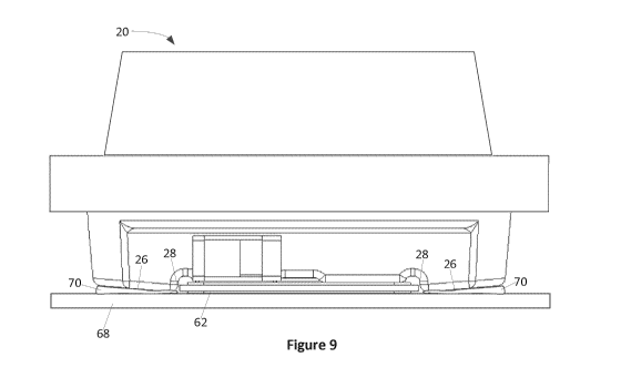
[0049] Figure 9 shows the SCA 32 secured to a backplate 68. The
underside
surfaces 26 of the SOE 20 are secured to the backplate 68 by a bonding agent
or
adhesive 70. Also, the heat conducting layer 62 of the SCA 32 is secured to
the
backplate 68. The backplate can be made of aluminum, plastic, or any other
suitable
material. The underside surface 26 are bonded (secured) directly to the
backplate. This
is to be understood as meaning that any gap between the underside surfaces 26
and the
backplate 68, can be filled, at least partially, with a bonding agent. The
underside
surfaces 26 need not physically touch the backplate 68 to be bonded directly
to the
backplate. The underside surfaces 26 being bonded directly to the backplate 68
also
applies to embodiments where at least a portion of the undersides surfaces are
in
physical contact with the backplate 68.
[0050] The adhesive 70 used to bond the underside surfaces 26 to the
backplate
68, or the SCA 32 to the backplate 68 can be, for example, a thermally
conductive epoxy,
a non-conductive epoxy, a thermally conductive silicone or a non-conductive
silicone.
Examples of thermally conductive epoxies include Masterbond SUP10AOHTTm,
SUP1OANHTTm; MG Chemicals 8331 Silver Conductive Epoxy Adhesive TM. Non-
conductive epoxies may include Dow D.E.H. 2OTM. Examples of Thermally
conductive
silicone adhesives include Dow Corning SE 4450 and Nusil R-2930TM. Examples
of
Non-conductive silicone adhesives can include Dow PV804TM. The adhesive used
to
bond the SOE 20 to the backplate 68 need not be the same as the adhesive used
to bond
the SCA 32 to the backplate 68. For example, a thermally conductive adhesive
can be
used to bond the SCA 32 to the backplate while a less specialized adhesive can
be used
to bond the SOE 32 to the backplate 68.
[0051] In some embodiments, prior to bonding the SOE 20 to the
backplate 68,
index matching material is placed over the solar cell 34 shown in Figure 7.
The amount
of index matching material is selected to fill the space between the solar
cell 34 and the
SOE 20 when the SOE is secured to the backplate 68. Any excess index matching
material can flow from between the solar cell 34 and the SOE 20 through the
indentation
31 shown in Figure 8.
[0052] In other embodiments, the SOE can be turned upside down and an index
matching material can be placed on the underside optical surface of the SOE.
The SCA
can be mated to the SOE and, the SCA and the SOE can be clamped to each other.
The
clamped SOE and SCA can then be flipped over (SOE on top, SCA on bottom). This
process allows bubbles in the silicone layer to migrate up and out of the
optical path,
8
CA 02895962 2015-06-19
WO 2014/094177
PCT/CA2013/051004
along the convex, underside optical surface of the SOE. Subsequently, the SCA
and the
SOE can be bonded to the backplate.
[0053] Figure 10 shows a gap 72 between the SOE 20 and the backplate
68.
This gap can measure 100 microns or any other suitable distance that allows
the SOE 20
to rest on the SCA 32.
[0054] Figure 11 shows a side view of an embodiment of the SOE 20 of
the
present disclosure. The side view shown at Figure 11 is from a viewpoint
located at 90
from the viewpoint of Figure 1. Shown in Figure 11 are the light input surface
22, one of
the underside surfaces 26, and walls 74.
[0055] Figure 12 shows the SOE 20 of Figure 11 optically and physically
coupled
to the SCA 32. The walls 74 are dimensioned and oriented (slanted) to allow
the SOE 20
be inserted and fitted between the surfaces 64 of the wire connectors 38. As
such, the
walls 74 of the SOE 20 and the surfaces 64 of the wire connectors 30 can
cooperate with
each other to self-align the SOE 20 to the SCA 32. In the present embodiment,
the walls
74 are alignment features of the SOE 20 and the surfaces 64 are alignment
features of
the SCA 32.
[0056] As shown in Figure 12, there is a gap between each wall 74 and
its
corresponding surface 64. These gaps are to allow the SOE 20 to rest on the
SCA 32
and to minimize strain applied by the walls 74 to the wire connectors 39 and
vice versa.
[0057] Figure 13 shows a perspective view of the SOE 20 self-aligned to the
SCA
32.
[0058] Figure 14 shows the SOE 20 of Figure 3A positioned (self-
aligned) with the
solar cell 34 of the SCA 32 of Figure 4. Also shown in Figure 14 is the
backplate 68. The
space (or volume) 150 between the SCA 32 and the SOE 20, and the space between
the
underside optical surface 35 and the solar cell 34, can be filled with an
index matching
material 152. The index matching material 152 can be, in some embodiments, an
optical
silicone such as, for example, Dow Sylgard 184TM, a two part silicone
elastomer, Dow
Sylgard 36636TM Silicone dielectric gel, and Dow 0E-6351, as well as Nu Sil,
Shin Etsu
and Henkel products. In other embodiments, non-curing silicone gels can be
used.
Examples of such non-curing silicone gels Dow 0E-6250 and Dow 0E-6450
[0059] As shown in Figure 14 the underside optical surface 35 is spaced-
apart
from the solar cell 34, which effectively avoids any shear stress between the
underside
optical surface 35 and the solar cell 34.
[0060] Figure 15 shows a side cross-sectional view of another
embodiment of a
SOE 120 of the present disclosure bonded directly on a backplate 68 and
overlapping the
9
CA 02895962 2015-06-19
WO 2014/094177
PCT/CA2013/051004
SCA 32. The SOE 100 has a light input surface 22 that receives light from a
primary
optical element (not shown). The SOE 20 concentrates the light onto the solar
cell 34.
[0061] The SOE 120 has underside surfaces 126, which can also be
referred to
as non-optical surfaces or areas. Contrary to other embodiments, the
embodiment of
Figure 15 provides no gap between the underside surfaces 126 and the backplate
68.
Further, in the present embodiment, there is no requirement to have the SOE
120 rest on
the SCA 32.
[0062] The SOE 120 has inboard surfaces 128 that cooperate with the
sidewalls
54 of the SCA 32 to self-register (self-align) the SOE 120 to the SCA 32 and
to the solar
cell 34.
[0063] The SOE being self-registered to the SCA is to be understood as
meaning
that the SOE is optically aligned with the solar cell of the SCA simply by
placing the SOE
over the SCA such that one or more of the alignment features of the SOE
cooperate with
one or more of the alignment features of the SCA to align, optically, the SOE
to the solar
cell. For example, referring to Figure 8, the SOE 20 can be self-registered to
the SCA 32
simply by placing the SOE 20 over the SCA 32 such that the inboard surfaces 28
of the
SOE 20 abut or overlap the side surfaces 52 and 54 of the SCA 32. The SOE 20
is also
self-aligned to the SCA 32 by virtue of the walls 74 of the SOE 20 being
placed adjacent
the surfaces 64 of the wire connectors 38, as shown at Figure 12. The
manufacturing
tolerances can be such that the SOE 20 will be optically coupled to the solar
cell of the
SCA 32 regardless of the inboard surfaces 28 abutting the side surfaces 52 and
54 or
simply being adjacent the side surfaces 52 and 54. As an example,
manufacturing
tolerance with respect to length and widths can vary between 0.1 mm to 0.15
mm.
[0064] Within the context of the present disclosure, the expression
"substantially
abut" is to be understood as meaning, for example, that an alignment feature
of the SOE
is abutting (is in contact with) an alignment feature of the SCA or that the
alignment
feature of the SOE is not quite abutting the alignment feature of the SCA but
the SOE is
nevertheless optically aligned with the solar cell of the SCA. As an example,
Figure 8
shows the inboard surfaces 28 of the SOE 20 not quite in contact with the side
surfaces
52 and 54 of the SCA 32; however, as the SOE 20 is aligned with the solar
cell, it can be
said that the inboard surfaces 28 substantially abut (or are substantially in
contact with)
respective side surfaces 52 and 54.
[0065] The examples presented above had, as alignment features, inboard
surfaces of an SOE and side surfaces of an SCA. However, any other suitable
alignment
feature defined on the SOE and the SCA are to be considered within the scope
of the
CA 02895962 2015-06-19
WO 2014/094177
PCT/CA2013/051004
present disclosure. For example one of the SCA and the SOE could have one or
more
boss that could fit into (cooperate with) corresponding one or more dimples
(indentation)
on the other of the SCA and the SOE to align the SOE to the SCA.
[0066] Examples presented above showed the SOE bonded directly to the
backplate. This need not always be the case. In some other embodiments, the
SOE can
be self-aligned to the SCA as described elsewhere in the disclosure, and can
be bonded
to the SCA itself rather than to the backplate. Figure 16 shows an example of
the SOE
20 being self-aligned with the SCA 32 and being bonded, with an adhesive (not
shown) to
the SCA 32 along the level surface 27.
[0067] In the context of the present disclosure, the temperature cycling
experienced by the backplate 68 is less than that experienced by the upper
metalized
surface of the SCA 32. By bonding the SOE 20 or 120 to the backplate 68
instead of the
SCA, there is reduction in the thermally-induced stress SOE and the SCA. This
enhances
the lifetime of the bond, leading to greater system reliability.
[0068] The new optical train and SOE of the present disclosure provide a
low-
carbon efficient energy CPV system which is inexpensive to manufacture, to
respond to
the energy needs of expanding markets.
[0069] As an example, the new optical train can be part of a CPV
module.
multiple CPV modules can then be mounted on dual-axis trackers. The footprint
of the
modular system is 4.8 m x 3.4 m, with an expected power output of over 5 kW.
Each
module is based on 40% high-efficiency, temperature-resistant, triple-junction
solar cells.
These cells split the solar spectrum into three specifically designed subcells
that
maximise the conversion of solar energy to electricity.
[0070] In some embodiments, the optical train can include a laminated
PMMA
Fresnel lens primary optic coupled to a four-lobe Kohler secondary optic that
has been
designed to minimize production costs while maximizing manufacturing
tolerances and
optical efficiency. The cell and SOE are mounted directly to the aluminium
backplate
isolating the requirements of mechanical and optical coupling and minimizing
the potential
for alignment error. The advanced optical train and mounting design allows for
the use of
a thermoset polymer casing which greatly reduces weight and cost.
[0071] The rear side of the backplate can be functionalized with a high
emissivity
thin-film coating that significantly lowers the cell operating temperature.
[0072] Advantageously, bonding the SOE 22 to the backplate or, in some
embodiments, to the SCA, and not to the solar cell itself can minimize the
opportunity for
optical misalignment in the assembly process. Also advantageously, bonding the
SOE to
11
CA 02895962 2015-06-19
WO 2014/094177
PCT/CA2013/051004
the backplate (or SCA) can allow for the bypass diode to be completely covered
by non-
optical parts of the SOE. That is, the bypass diode receives little light.
This provides a
shield against damage to the bypass diode caused by stray light during off
axis events.
This removes the need for an expensive/heavy shield layer of the bypass diode.
[0073] Figure 17 shows a side, cross-sectional view of an embodiment of a
CPV
module of the present disclosure. Shown in Figure 17 is a primary optical
element 500,
the SOE 20 that receives light from the primary optical element 500, the SCA
32, which
has a solar cell that receives light from the SOE 20, and the backplate 68
onto which the
SCA 32 and the SOE are bonded.
[0074] In general, and in the context of the present disclosure, two
components
are "electrically connected" when an electrical change caused by or affecting
one (such
as a change in voltage or current) can result in an electrical change in the
other, or when
an electrical signal sent by one can be received by the other. The two
components need
not be directly electrically connected (that is, there may be other elements
interposed
between them), and they may be, but need not be, proximate to one another.
"Electrically
connected" also includes the concept that components may be physically
connected but
the electrical circuit connections between them may be broken or completed by,
for
example, switching circuitry.
[0075] Further, in general, and in the context of the present
disclosure, two
components are optically coupled when a change in light at one component (such
as a
change in light intensity) can result in a change in light at the other, or
when an optical
signal stemming from one can be received by the other. Furthermore, two
components
are optically aligned when a majority of light stemming from one is received
by the other
or, when light intensity received at one component is within a pre-determined
acceptable
range or target range, or is equal to, or greater than, a target value. For
example, given a
standard light input, an SOE can be said to be optically aligned with a solar
cell when the
electrical signal generated at the solar cell by the light received at the
solar cell from the
SOE is equal to, or greater than, a target electrical signal value.
[0076] In the preceding description, for purposes of explanation,
numerous details
are set forth in order to provide a thorough understanding of the embodiments.
However,
it will be apparent to one skilled in the art that these specific details are
not required. In
other instances, well-known electrical structures and circuits are shown in
block diagram
form in order not to obscure the understanding.
[0077] The above-described embodiments are intended to be examples
only.
Alterations, modifications and variations can be effected to the particular
embodiments by
12
CA 02895962 2015-06-19
WO 2014/094177
PCT/CA2013/051004
those of skill in the art without departing from the scope, which is defined
solely by the
claims appended hereto.
13