Note: Descriptions are shown in the official language in which they were submitted.
CA 02907472 2015-09-17
WO 2014/161080
PCT/CA2014/000325
1
COMMUTATION CELL AND COMPENSATION CIRCUIT
THEREFOR
TECHNICAL FIELD
[0001] The present disclosure relates to the field of power
electronics.
More specifically, the present disclosure relates to a commutation cell
configured for limiting switching overvoltage at turn-on and turn-off of the
power electronic switch and for controlling the recovery current in a
freewheel
diode of the commutation cell at turn-on of the power electronic switch. The
present disclosure further relates to a compensation circuit for use in a
commutation cell and to a power converter including the commutation cell with
the compensation circuit.
BACKGROUND
[0002] Commutation cells are commonly used in electronic systems
that require conversion of a voltage source, including both DC-DC converters
and DC-AC converters, which are often called inverters. With the limited space
allowed for power converter circuits, such as those used for example in
electric
and/or electric hybrid automotive applications, and given the high cost of the
semi-conductors, the demand for integration of these commutation cells
increases.
[0003] A known way of reducing the space occupied by
semiconductors in power converter circuits is to increase their efficiency to
allow the size of the cooling surface to be reduced.
[0004] Losses in power electronic switches present in conventional
power converter circuits are mainly caused by two sources; conduction losses
and switching losses. One way to reduce switching losses is generally by
accelerating turn-on and turn-off of the power electronic switches. However,
fast turn-off of the power electronic switches generates overvoltage in stray
inductances of their high-frequency loop. It is thus often required to slow
down
CA 02907472 2015-09-17
WO 2014/161080
PCT/CA2014/000325
2
turning off of the power electronic switches to protect them against
overvoltage. This may seriously impact the overall efficiency of conventional
power converter circuits.
[0005] Figure 1 is an idealized circuit diagram of a conventional
commutation cell such as those used in conventional power converter circuits.
A commutation cell 10 converts a DC voltage Vbõ from a voltage source 12 (or
from a capacitor) into a current source /out (or into an inductance) that
usually
generates a voltage Vout appropriate for a load 14, which may be a resistive
load, an electric motor, and the like. The commutation cell 10 comprises a
freewheel diode 16 and a controlled power electronic switch 18, for example
an isolated gate bipolar transistor (IGBT). A capacitor 20 (Cm) is used to
limit
variations of the voltage Vbus of the voltage source 12 and an inductance 32
is
used to limit the variations of the output current /õt. A gate driver (not
shown in
Figure 1 but shown on later Figures) controls turning on and off of the power
electronic switch 18. Figure 1 illustrates a configuration of the commutation
cell
10, of the load 14, and of the voltage source 12, in which energy flows from
the
voltage source 12 to the load 14, i.e. from left to right on the drawing. The
commutation cell 10 can also be used in a reverse configuration in which
energy flows in the opposite direction.
[0006] When turned on, the power electronic switch 18 allows current
to pass therethrough, from its collector 22 to its emitter 24. The power
electronic switch 18 can be approximated as a closed circuit. When turned off,
the power electronic switch 18 does not allow current to pass therethrough and
becomes an open circuit.
[0007] The gate driver applies a variable control voltage between the
gate 26 and the emitter 24 of the power electronic switch 18. For some types
of power electronic switches such as bipolar transistors, the gate driver may
act as a current source instead of as a voltage source. Generally, when the
voltage applied between the gate 26 and the emitter 24 is "high", the power
electronic switch 18 allows passing of current from the collector 22 to the
CA 02907472 2015-09-17
WO 2014/161080
PCT/CA2014/000325
3
emitter 24. When the voltage applied between the gate 26 and the emitter 24 is
"low", the power electronic switch 18 blocks passage of current therethrough.
In more details, a voltage difference between the gate 26 and the emitter 24,
denoted Vge, is controlled by the gate driver. When Vge is greater than a
threshold Vgeoto for the power electronic switch 18, the switch 18 is turned
on
and a voltage Vce between the collector 22 and the emitter 24 becomes near
zero. When Vge is lower than Vgeoto, the power electronic switch 18 is turned
off
and Voe eventually reaches Vbus=
[0008] When the power electronic switch 18 is turned on, a current
/out
flows from the voltage source 12 (and transiently from the capacitor 20)
through the load 14 and through the collector 22 and the emitter 24. When the
power electronic switch 18 is turned off, the current /out circulates from the
load
14 and passes in the freewheel diode 16. It may thus be observed that the
power electronic switch 18 and the freewheel diode 16 operate in tandem.
Turning on and off of the power electronic switch 18 at a high frequency
allows
the current /out, in the output inductance Lout 32, to remain fairly constant.
[0009] It should be observed that, in the case of other power
electronic switch types, for example bipolar transistors, the term "gate" may
be
replaced with "base", the base being controlled by a current as opposed to the
gate that is controlled by a voltage. These distinctions do not change the
overall operation principles of the commutation cell 10.
[0010] Figure 2 is another circuit diagram of the conventional
commutation cell of Figure 1, showing parasitic inductances. In contrast with
the idealized model of Figure 1, connections between components of an actual
commutation cell define parasitic (stray) inductances. Though the parasitic
inductances are distributed at various places within the commutation cell 10,
a
suitable model presented in Figure 2 shows two (2) distinct inductances
representing the overall parasitic inductance, including an emitter inductance
30 of the power electronic switch 18 and an inductance 34 representative of
all
other parasitic inductances (other than the emitter inductance 30) around a
CA 02907472 2015-09-17
WO 2014/161080
PCT/CA2014/000325
4
high frequency loop 36 formed by the freewheel diode 16, the power electronic
switch 18 and the capacitor 20. The high frequency loop 36 is a path where
current changes significantly upon switching of the power electronic switch
18.
It should be noted that an output inductance Lout 32 is not part of the high
frequency loop because its current remains fairly constant through the
commutation period.
[0011] Figure 3 is a circuit diagram of a conventional commutation
cell further showing a gate driver 40. Some elements of the commutation cell
are not shown on Figure 3, in order to simply the illustration. Figure 3
further shows a gate driver 40 having a positive supply voltage 42 and a
negative supply voltage 44, an output 46 of the gate driver 40 being connected
to the gate 26 of the power electronic switch 18 via a gate resistor Rg. The
positive supply voltage 42 of the gate driver 40 has a value denoted +Vco, for
example +15 volts above a ground reference (shown on a later Figure) while
the negative supply voltage 44 has value denoted -Vdd, for example -5 volts
below the ground reference. An input 50 of the gate driver 40 is connected to
a
controller (not shown) of the commutation cell 10, as is well known in the
art. A
voltage at the output 46 of the gate driver 40 goes up to +Voo and goes down
to
-Vdd in order to control the voltage at the gate 26. The input resistance of
the
gate 26 to emitter may be very high, especially in the case of an IGBT.
However, a parasitic capacitance Cge (shown on a later Figure), present
between the gate 26 and the emitter 24, causes some current to flow from the
output 46 when the gate driver 40 alternates between +Voc and -Vdd. The value
Rg of the gate resistor is selected as a function of the parasitic capacitance
Cge
and of a desired switching rate of the power electronic switch 18 so that the
voltage at the gate 26 changes at rate appropriate for the desired switching
rate.
[0012] On Figure 3, a current Lgot flowing through the power
electronic
switch 18 and through the emitter parasitic inductance 30 is essentially equal
to /out when the power electronic switch 18 is closed, and quickly reduces to
CA 02907472 2015-09-17
WO 2014/161080
PCT/CA2014/000325
zero (substantially) when the power electronic switch 18 turns off.
[0013] When the power electronic switch 18 turns on or off, the
current Lgbt flowing therethrough increases or diminishes at a fast rate.
These
variations of LW, denoted di/dt, generate voltage across inductances 30 and
34, according to the well-known equation (1):
di
(1)
[0014] wherein 1/,_ is a voltage induced across an inductance and L
is
an inductance value.
[0015] A voltage VLs is generated across the parasitic inductance 34
and a voltage VL, is generated across the emitter parasitic inductance 30. On
Figures 2 and 3, the polarities shown across the high frequency loop
inductance 34, including the emitter inductance 30 reflect voltages obtained
upon turn-off of the power electronic switch 18, when the Lgbt current
diminishes very rapidly, di/dt thus taking a negative value. Upon turn-on of
the
power electronic switch 18, voltages across the high frequency loop
inductance 34, including the emitter inductance 30 are in the opposite
direction.
[0016] These voltages k/Ls and 1/L9 are in series with Vbus from the
voltage source 12. When the power electronic switch 18 turns off, the
collector
22 to emitter 24 voltage increases until the freewheel diode 16 turns on. At
that
time, addition of Vbus, VLs and I/Le results in an important overvoltage
applied
between the collector 22 and the emitter 24 of the power electronic switch 18.
Though power electronic switches are rated for operation at some level of
voltage, extreme overvoltage can reduce the lifetime of any power electronic
switch to thereby lead to its premature failure or even break the device.
[0017] Figure 4 is a circuit diagram of a conventional IGBT leg
formed
of two conventional commutation cells. Two commutation cells 10 introduced in
the above description of Figures 1-3, in which IGBTs are used as power
electronic switches 18 in the example of Figure 4, are connected in a single
CA 02907472 2015-09-17
WO 2014/161080
PCT/CA2014/000325
6
loop to form an IGBT leg 70. A first power electronic switch (bottom IGBT Q./)
operates in tandem with a first freewheel diode (top freewheel diode 02) and a
second power electronic switch (top IGBT Q2) operates in tandem with another
freewheel diode (bottom freewheel diode Dl). Each IGBT has its own gate
driver 40. A voltage source (not shown) provides a voltage Vbõ in parallel to
an
input capacitance 20 (Cm) connected to the IGBT leg 70 via a parasitic
inductance L. Inductances inherently provided in wires, connections,
decoupling capacitor and circuit board traces of a power converter have been
represented in Figure 4. A three-phase power converter used for powering a
three-phase electric motor (not shown) from a battery (also not shown), would
comprise three (3) IGBT legs 70 as shown on Figure 4. Since such power
converters are believed well-known, they are not described in further details
herein.
[0018] As can be seen from Figure 4, a reference of each gate driver
is connected to the emitter of the IGBT Q1 and Q2, typically known as logical
pins of the IGBTs Ql and Q2. For concision purpose, a description of Figure 4
focuses on its bottom portion including the bottom IGBT Q1.
[0019] The overvoltage effect on a power electronic switch 18,
discussed in the above description of Figures 2 and 3, also applies to the
IGBTs Q1 and Q2.When the bottom IGBT Q1 is turned off, current transits from
the bottom IGBT Qi to the top freewheel diode 02, during an overvoltage
period. A properly selected IGBT is able to support the overvoltage created by
a current variation (c/i/dt) across various parasitic inductances (La, L+Vbus,
Lc-high,
Le-high, Lc-low, Le-low and Lvb,$) present in the IGBT leg 70. Indeed, since
the
inductances resist change of current therein, additive voltages develop in the
IGBT leg 70 as illustrated by the polarities of the parasitic inductances
shown
on in Figure 4. These voltages, added to the voltage Vbus of the source, often
result in a voltage exceeding the maximal collector to emitter voltage lice
rating
of the bottom IGBT Q1. The top IGBT Q2 is subject to the same problem.
[0020] Figure 5 is a diagram showing current and voltage waveforms
CA 02907472 2015-09-17
WO 2014/161080
PCT/CA2014/000325
7
at turn-off of the IGBTs of Figure 4. The collector to emitter voltage lice,
the
gate to emitter voltage Vge and a current / flowing from the collector to the
emitter of the IGBT Q./ are shown at turn-off. It may be observed that there
is
a major overvoltage (peak) of lice, above the voltage of the source Vbõ,, at
the
time of turn-off.
[0021] Solutions exist that tend to limit overvoltage in power
electronic
switches by slowing down the slope of the gate-emitter voltage. However,
excessive limitation of the overvoltage can imply longer switching times of
the
current, reducing commutation cell performance.
[0022] Also, when the power electronic switch 18 turns on, current
starts flowing between the collector 22 and the emitter 24. Current flowing
through the freewheel diode 16 concurrently diminishes until the entire
current
/õt flows through the power electronic switch 18. An additional current,
called a
recovery current, circulates in the power electronic switch 18 so that some
current circulates in the reverse direction of the freewheel diode 16 until
all
charges deposited on its junction are removed. The freewheel diode 16 then
turns off, allowing voltage to build thereon while voltage between the
collector
22 and the emitter 24 of the power electronic switch 18 reduces substantially
to
zero. When the freewheel diode 16 blocks, the reverse flowing current causes
an abrupt voltage increase that in turn causes oscillations between a
parasitic
capacitance (not explicitly shown) of the freewheel diode 16 and inductances
30 and 34 of the high frequency loop 36.
[0023] It is thus important to control the di/dt when turning on the
power electronic switch 18 since an excessively abrupt drop in voltage could
inject current in the gate of an opposite power electronic switch (not shown),
causing the opposite power electronic switch to become conductive while the
power electronic switch 18 is still conductive. The di/dt also generates
important and undesirable electromagnetic interference (EMI).
[0024] Therefore, there is a need for methods and circuits capable of
reducing overvoltage occurring upon switching in commutation cells and to
CA 02907472 2015-09-17
WO 2014/161080
PCT/CA2014/000325
8
control the di/dt at turn-on of the power electronic switch without undue
switching delays.
SUMMARY
[0025] According to the present disclosure, there is provided a
commutation cell configured for limiting switching overvoltage and for
limiting
recovery current. The commutation cell comprises a power electronic switch
having a parasitic emitter inductance through which a voltage is generated
upon turning on and off of the power electronic switch. The commutation cell
also comprises a compensation circuit connected to the parasitic emitter
inductance. The compensation circuit applies a sample of the voltage
generated through the parasitic emitter inductance at turn-on and turn-off of
the power electronic switch to control the voltage generated through the
parasitic emitter inductance.
[0026] According to the present disclosure, there is also provided a
power converter, comprising two of the commutation cells configured for
limiting switching overvoltage and for limiting recovery current. The two
commutation cells form a loop and are connected at a junction of a collector
of
a first power electronic switch of a first commutation cell and of an emitter
of a
second power electronic switch of a second commutation cell.
[0027] The present disclosure further relates to a compensation
circuit for limiting switching overvoltage on a power electronic switch of a
commutation cell, the commutation cell including a high frequency loop having
a parasitic inductance through which a voltage is generated upon turning off
of
the power electronic switch, the high frequency loop parasitic inductance
including a parasitic emitter inductance of the power electronic switch. The
compensation circuit comprises a voltage divider configured to provide a gain
of a voltage generated on the parasitic emitter inductance at turn-on and at
turn-off of the power electronic switch. The compensation circuit also
comprises a connection from the voltage divider to provide a feedback voltage
CA 02907472 2015-09-17
WO 2014/161080
PCT/CA2014/000325
9
to the power electronic switch gate driver according to the gain to reduce the
voltage generated on the parasitic inductance of the high frequency loop.
[0028] The foregoing and other features will become more apparent
upon reading of the following non-restrictive description of illustrative
embodiments thereof, given by way of example only with reference to the
accompanying drawings.
BRIEF DESCRIPTION OF THE DRAWINGS
[0029] Embodiments of the disclosure will be described by way of
example only with reference to the accompanying drawings, in which:
[0030] Figure 1 is an idealized circuit diagram of a conventional
commutation cell such as those used in conventional power
converter circuits;
[0031] Figure 2 is another circuit diagram of the conventional
commutation cell of Figure 1, showing parasitic inductances;
[0032] Figure 3 is a circuit diagram of a conventional commutation
cell further showing a gate driver;
[0033] Figure 4 is a circuit diagram of a conventional IGBT leg formed
of two conventional commutation cells;
[0034] Figure 5 is a diagram showing current and voltage waveforms
at turn-off of the IGBTs of Figure 4;
[0035] Figure 6 is a circuit diagram of an IGBT leg having resistive
dividers connected across stray emitter inductances, according
to an embodiment;
[0036] Figure 7 is a diagram showing current and voltage waveforms
at turn-off of the IGBTs of Figure 6 with a bus voltage of 500
volts;
[0037] Figure 8 is a diagram showing current and voltage waveforms
CA 02907472 2015-09-17
WO 2014/161080
PCT/CA2014/000325
at turn-off of the IGBTs of Figure 6, the resistive divider being
adjusted for a maximum bus voltage of 300 volts in short
circuit condition;
[0038] Figure 9 is a circuit diagram of an IGBT leg using a
transformer to increase an apparent emitter inductance,
according to another embodiment;
[0039] Figure 10 is a variant of the circuit diagram of Figure 9
using a
transformer and a resistive device, according to a further
embodiment;
[0040] Figure 11 is a schematic layout for an IGBT leg having a
connector for adjusting a top emitter inductance according to a
first variant;
[0041] Figure 12 is a schematic layout for an IGBT leg having a
connector for adjusting a top emitter inductance according to a
second variant;
[0042] Figure 13 is a schematic representation of IGBT capacitances
including a Miller Capacitance;
[0043] Figure 14 is an illustration of an equivalent circuit of a
typical
IGBT;
[0044] Figure 15 is a graph showing wave shapes of the current
through a IGBT and a collector to emitter voltage of the IGBT;
[0045] Figure 16 is a diagram of a commutation cell having a circuit
for limiting overvoltage at turn-off of the power electronic
switch and recovery current at turn-on of the power electronic
switch, when the freewheel diode turns-off, according to an
illustrative embodiment;
[0046] Figure 17 is a small signal control loop model of the
commutation cell of Figure 16 at turn-off of the power
CA 02907472 2015-09-17
WO 2014/161080
PCT/CA2014/000325
11
electronic switch;
[0047] Figure 18 is a small signal control loop model of the
commutation cell of Figure 16 at turn-on of the power
electronic switch;
[0048] Figure 19 is a partial circuit diagram of an IGBT leg that
incorporates the circuit for limiting turn-off overvoltage and
turn-on recovery current of Figure 16;
[0049] Figure 20 is a graphic illustrating recovery current of a
freewheel diode without the circuit for limiting turn-off
overvoltage and turn-on recovery current, with a very high
di/dt;
[0050] Figure 21 is a graphic illustrating recovery current of the
freewheel diode of Figure 19;
[0051] Figure 22 is a graphic illustrating a comparison of output
currents as a function of bus voltages that can be provided
with and without the circuit for limiting turn-off overvoltage and
turn-on recovery current; and
[0052] Figure 23 is a graphic illustrating the output current as a
function of switching frequency using the circuit for limiting
turn-off overvoltage and turn-on recovery current.
DETAILED DESCRIPTION
[0053] Like numerals represent like features on the various drawings.
[0054] Various aspects of the present disclosure generally address
one or more of the problems of overvoltage and recovery current present in
commutation cells at the time of switching.
[0055] Circuits operable to limit overvoltage in commutation cells,
especially at turn-off of IGBTs, are described in international patent
publication
CA 02907472 2016-12-22
12
no WO 2013/082705 Al, in international patent application no
PCT/CA2013/000805, in US provisional applications no 61/808,254 and no
61/904,038, and in "Reducing switching losses and increasing IGBT drive
efficiency with ReflexTM gate driver technology", available at
http://www.advbe.com/docs/DeciElec2013-Jean Marc Cyr-TM4.pdf, all of
which are authored by Jean-Marc Cyr et al.
[0056] The present technology provides control of overvoltage and
switching losses at turn-on and turn-on as well as a reduction of recovery
current at turn-on of a power electronic switch of a commutation cell.
Circuits
and methods presented herein are generally compatible with solutions to limit
overvoltage at turn-off of power electronic switches.
[0057] In a commutation cell, di/dt at turn-off of a power electronic
switch generates a voltage across stray inductances of a high frequency loop
of the commutation cell. This voltage is applied across the power electronic
switch in addition to a bus voltage providing power to the commutation cell.
The present disclosure introduces a solution based on the injection of a
sample of the overvoltage present across the power electronic switch to a gate
driver of the power electronic switch. This injection slows down a variation
of
the gate voltage. This, in turn, decreases an amount overvoltage on the power
electronic switch. The effect can be limited to only occur during a period
when
the overvoltage is above a predetermined value. By precisely controlling the
di/dt, overvoltage of the power electronic switch can be controlled while an
opposite freewheel diode operating in tandem with power electronic switch
turns off. This technique allows the power electronic switch to be rapidly
turned
on while preventing damage due to overvoltage.
[0058] The techniques disclosed herein will mainly be described in
relation to the use of isolated gate bipolar transistors (IGBT). Mentions of
IGBTs in the following description are made for illustration purposes and are
not meant to limit the present disclosure. The same techniques may equally be
4960318.1
CA 02907472 2015-09-17
WO 2014/161080
PCT/CA2014/000325
13
applied to commutation cells constructed using metal¨oxide¨semiconductor
field-effect transistors (MOSFET), bipolar transistors and like power
electronic
switches.
[0059] Generally stated, by changing the reference of the gate driver
from the emitter (logical pin) of Figure 4 to the ground bus (for the bottom
IGBT
Qi) and to the collector of the bottom IGBT (for the top IGBT Q2), it is
possible
to decrease this overvoltage of Võ during turn-off.
[0060] In other words, a technique for connecting reference of the
gate driver to a power tab of the IGBT, the power tab being itself connected
to
a power source, instead of to the logical pin has been developed. A voltage
across the emitter inductance is injected in the gate driver to create a
negative
voltage at the emitter of the IGBT to slow down the negative slope of Vge, as
will be discussed hereinbelow. The result is a direct action on the gate
voltage
without any delay and di/dt limitations.
[0061] Because there is no optimal emitter inductance between the
logical and power connections of the emitter in a commercial IGBT module, the
present disclosure introduces a technique developed to optimize the sample of
the overvoltage injected in the gate drive circuit using a resistive divider.
Figure
6 is a circuit diagram of an IGBT leg having resistive dividers connected
across
stray emitter inductances, according to an embodiment. Generally, Figure 6
shows an IGBT leg 90 including compensation circuits connected to gate
drivers 40 in a configuration that reduces overvoltage on the IGBTs. Figure 6
introduces a compensation circuit that optimizes overvoltage on the IGBT
using a resistive divider.
[0062] Discussing the bottom portion of the IGBT leg 90 of Figure 6,
the bottom IGBT Q1 includes has a parasitic collector inductance l_c-10w, a
parasitic emitter inductance Le-low. The gate of the bottom IGBT Q1 connected
to its gate driver 40 via a resistor R1. A reference 52 of the gate driver 40
is
connected to a compensation circuit having a resistive divider circuit
including
two resistors R2 and R3 and a diode D3 that allows the turn-on not to be
CA 02907472 2015-09-17
WO 2014/161080
PCT/CA2014/000325
14
impacted by shorting the resistor R2 when a voltage at the emitter of the
bottom IGBT Q1 is higher than the reference 52.
[0063] In the circuit of Figure 6, values of the resistors R2 and R3
are
selected according to an acceptable overvoltage level allowed across the
bottom IGBT Q1. Figure 7 is a diagram showing current and voltage waveforms
at turn-off of the IGBTs of Figure 6 with a bus voltage of 500 volts. Figure 8
is a
diagram showing current and voltage waveforms at turn-off of the IGBTs of
Figure 6, the resistive divider being adjusted for a maximum bus voltage of
300
volts in short circuit condition. A ratio of R2 over R3 is increased to reduce
the
overvoltage. The value of these two resistors R2 and R3 in parallel is set, in
series with a gate driver resistor R1. A value of the gate driver resistor R/
is
adjusted in a conventional manner according to a proper commutation
behavior.
[0064] By correctly setting values of the resistors of the
compensation
circuits, it is possible to reduce the effect of the emitter inductance to get
the
maximum overvoltage allowed to therefore improve the efficiency.
[0065] In other words, the normal practice consisting in using a
resistor R1 in the ground connection of the gate driver to limit the current
in the
diodes that protect the gate driver of the lower IGBT from a negative voltage
when the upper IGBT turns off has been modified by splitting the resistor in
two
resistors, including R1 in series with R2 and R3 connected in parallel, and by
adapting their ratio to limit the effect of the emitter inductance on the
di/dt. An
equivalent resistor value may remain the same, but the voltage divider gives
the desired weight of the emitter inductance to limit the overvoltage at the
desired level.
[0066] The overvoltage can be optimized as much as possible to
reach the maximum IGBT rating. This is done by reducing a value of R2, the
resistor connected to the IGBT emitter, compared to R3, the resistor connected
to the power tab. The voltage across the emitter inductance will be split in
two
and only the voltage across the logical resistor will be applied in the gate
drive
CA 02907472 2015-09-17
WO 2014/161080
PCT/CA2014/000325
circuit to limit the gate voltage drop.
[0067] Figures 7 and 8 both show the current / and the voltages Vge
and Võ during turn-off for the circuit of Figure 6, for different bus
voltages. It
may be observed that overvoltage of Võ during turn-off is greatly reduced (see
plateau 24). This plateau 24 occurs while a drop rate of the voltage Vge is
reduced by the insertion of a sample of the voltage across the parasitic
inductance Le-iow=
[0068] The duration of the plateau 92 impacts losses of the
commutation cell during turn-off of the IGBT. A longer plateau 92 brings
higher
losses. Because of the desire to limit at the same time the overvoltage and
its
length, a square wave shape of the overvoltage plateau 92 is suitable. The
intrinsic behavior (natural feedback) of the overvoltage gives this shape.
[0069] This technique works very well for the bottom IGBT Q1
because the emitter inductance Le-low is sufficiently large to provide good
overvoltage sampling. In contrast, for the top IGBT Q2, the emitter inductance
Le-high often has a too small value to suitably clamp a voltage thereacross
without increasing the gate resistor R3, to protect the top IGBT Q2. In
practice,
the emitter inductance Le-high of the top IGBT Q2 is very often too low to be
used to bring down the overvoltage across the top IGBT Q2 to a safe level.
[0070] Indeed, because of the constraints on packaging of IGBT
modules, the upper and lower semiconductors are packaged within close
proximity of each other so the inductance of the upper IGBT Q2, Le-high, is
quite
small, in the order of a few nH. On the other hand, because the only point of
connection other than the logical emitter of the lower IGBT Q1 is the power
tab
of -Vbus, the inductance of the lower IGBT al, Le-low, may be as much as 5
times the upper emitter inductance Lehigh. The connection of the -Vbus tab is
highly inductive because of its length and curves.
[0071] In other words, IGBT modules have two power connections,
part of the high-frequency loop, that are the most inductive, including a
+Vbus
CA 02907472 2015-09-17
WO 2014/161080
PCT/CA2014/000325
16
tab and a -Vbõ tab. Because the -Vbõ tab is in the path of the emitter of the
bottom IGBT C/1, it can be used in the manner described hereinabove to inject
a sample of the overvoltage across the IGBT Q./ in the gate driver of the
bottom IGBT Qi. However, since the +Vbus tab is connected to the collector of
the top IGBT Q2, this inductance cannot be used directly as a feedback in the
gate driver.
[0072] To use the
Le-high inductance as a source of feedback in the
gate driver of the top IGBT Q2, there is a need to somehow increase its
apparent inductance without unduly increasing the overall inductance of the
high frequency loop. Two
possible techniques to increase the Lehigh
inductance will be described hereinbelow.
[0073] In order
to optimize the top IGBT Q2 turn-off, a first technique
using the collector parasitic inductance to inject a sample of the overvoltage
across the top IGBT Q2 using a transformer to isolate the collector from the
emitter has been designed. This technique is illustrated in Figure 9, which is
a
circuit diagram of an IGBT leg using a transformer to increase an apparent
emitter inductance, according to another embodiment. The transformer is used
to reduce overvoltage on the top IGBT Q2. A primary Tia of the transformer is
connected across the parasitic inductance Lc-high of the top IGBT Q2. A
secondary Tia of the transformer is connected in series with a resistor R5,
which is connected further to a ground reference to a gate driver of the top
IGBT Q2. The primary Tia and the secondary Tia are connected so that when a
current Lgbt flowing through the top IGBT Q2 is decreasing at turn-off, a
voltage
having a polarity as shown on Figure 9 is generated across both the parasitic
inductance Lc-htgh and the primary Tra. The transformer causes a voltage
having another polarity as shown on Figure 9 to be generated across the
primary Tlb=
[0074] Therefore,
a negative voltage that appears across the
transformer when the current decrease in the top IGBT Q2 is used to cause a
negative voltage applied at the emitter of the top IGBT Q2 to slow down the
CA 02907472 2015-09-17
WO 2014/161080
PCT/CA2014/000325
17
slope of its gate voltage. Control of the overvoltage for the top IGBT Q2 can
thus be performed by properly selecting a turn ratio of the transformer.
[0075] It may be observed that the operating principle of the circuit
of
Figure 9 is quite similar to that of the circuit of Figure 6. The parasitic
inductance Lehigh of the emitter of the top IGBT Q2 not being sufficient to
properly slow down the negative lice slope of at turn-off the top IGBT Q2
using
the technique of Figure 6, a sample of the parasitic inductance Lc..high of
the
collector of the top IGBT Q2 is placed in series with parasitic inductance Le-
high
through the transformer.
[0076] Figure 10 is a variant of the circuit diagram of Figure 9
using a
transformer and a resistive device, according to a further embodiment. In this
variant, reduction of the overvoltage on the top IGBT Q2 is made by using the
transformer in addition to a resistive divider. The resistive divider includes
resistors R5 and R6 connected in a manner similar to resistors R2 and R3 used
to control overvoltage of the bottom IGBT Q1. Otherwise stated, Figure 10
combines the features of Figures 6 and 9 to enable fine tuning of the shape of
the negative slope of the Vge on the top IGBT Q2.
[0077] A further technique to increase the emitter inductance of the
top IGBT Q2 will now be described in Figures 11 and 12, which are schematic
layouts for IGBT legs having connectors for adjusting top emitter inductances
according to first and second variants. These layouts may be used to build
three (3) IGBT legs as illustrated in Figure 6, forming a power converter, or
inverter, providing three-phase AC current to a load. As will be explained
hereinbelow, the parasitic inductance Le-high is made adjustable by
configuration of the connectors.
[0078] Increasing the parasitic inductance of the top IGBTs Q2 may
have an impact on the inductance of the total high frequency loop of the IGBT
legs. However, impacts of this parasitic inductance on the control of the
overvoltage are much more significant. Figure 11 is a schematic layout for an
IGBT leg 90 having a connector for adjusting a top emitter inductance
CA 02907472 2015-09-17
WO 2014/161080
PCT/CA2014/000325
18
according to a first variant. On Figure 11, three (3) top IGBTs Q2 are mounted
on areas 102 and three (3) bottom IGBTs Q/ are mounted on areas 112. Each
top IGBTs Q2 has a collector mounted to a trace 104, identified on Figure 11
as C-High. Emitters of the top IGBTs Q2 are connected to emitter pads 106 via
wire bonds 110. Similarly, each bottom IGBT Q1 has a collector mounted to a
trace 114 identified on Figure 11 as C-Low. Emitters of the bottom IGBTs Q1
are connected to a trace 118 via wire bonds 120, the trace 118 being referred
to as E-Low. The trace 114 also has collector pads 116 that are connected
thereto.
[0079] A + Vbus tab 122 is connected to trace 104 while A -Vbus tab
124
is connected to trace 118. A phase tab 126 for connecting a load to the power
converter is connected to trace 114. The gates of the IGBTs mounted on
areas 102 and 112 are not shown in Figure 11 in order to simplify the
illustration.
[0080] The pads 106 and 116 are interconnected by a U-shaped
connector 128 having six (6) legs 130 so configured, sized and positioned as
to connect to the pads 106 and 116. The U-shaped connector 128 defines at
least in part the parasitic inductance Le_high since it interconnects emitters
of the
top IGBTs Q2 and collectors of the bottom IGBTs Ql. Since the U-shape
connector 128 is relatively large and includes right angles, the Le-high
inductance is relatively high and can be used to limit the overvoltage in the
top
IGBTs Q2 as discussed hereinabove. The size and shape of the connector
128 may be determined according to the desired parasitic inductance required.
[0081] Turning now to Figure 12, which is a schematic layout for an
IGBT leg having a connector for adjusting a top emitter inductance according
to a second variant, a main difference between the shown layout and the
layout of Figure 11 and the layout of Figure 12 lies in the position of the
pads
106. On Figure 12, the pads 106 are positioned farther away from the pads
116 to provide added space for a larger connector 132. The larger connector
132 of Figure 12 confers a larger parasitic inductance Le-high to the layout
of
CA 02907472 2015-09-17
WO 2014/161080
PCT/CA2014/000325
19
Figure 12.
[0082] It is desired to reducing switching losses at turn-on of a
power
electronic switch. Even if the turn-on overvoltage across one IGBT is not as
high the overvoltage across the opposite IGBT at turn-off, there is a limit
above
which a parasitic capacitance CCG between the collector and the gate (called a
Miller capacitance) of the IGBT being turned on will inject enough current in
its
gate to turn it on and create a cross conduction.
[0083] Figure 13 is a schematic representation of IGBT capacitances
including a Miller Capacitance. A Miller current 200 circulates in the Miller
capacitance CCG, causing a voltage variation dv/dt thereacross. The Miller
current 200 is split between a portion 202 flowing through a gate resistance
RG0ff and a portion 204 flowing through a gate to emitter parasitic
capacitance
CGE. The gate driver tries to maintain the gate to emitter voltage Vge in an
off
state, sinking the current 202 with the gate resistor RGeff. To this end, the
gate
resistor RGoff has a low value to keep the gate to emitter voltage Vge below
the
threshold voltage Vget(h) even in the presence of the Miller current.
[0084] Previously described Figure 10 shows the current Lgbt flowing
through the top IGBT Q2. In another phase, the top IGBT Q2 turns off and a
similar current flows through bottom IGBT Q1. These current has negative di/dt
at turn-off of the respective IGBTs. The polarity of the voltages generated
across the two emitter inductances Le-high and Le-low, upon turn-off of the
respective IGBT, and across the primary Tr, of the transformer in the case of
the top IGBT Q2, tend to maintain the IGBTs on during their turn-off process.
These voltages slow down the variation of the gate to emitter voltage Vge of
the
IGBTs being turned off but also tend to turn on the opposite IGBT. This has
limited impact because it happens while current has started to circulate in
the
freewheel diodes. The voltage across the IGBT mounted in parallel to the
freewheel diode having become conductive is zero. When one IGBT turns on,
the voltage across its emitter inductance is also opposite to the gate signal
so
CA 02907472 2015-09-17
WO 2014/161080
PCT/CA2014/000325
the net effect is a tendency to keep the IGBT turned off. The present
technology increases the immunity of the dv/dt of the \ice to keep one IGBT
off
during the turn-on process of the opposite IGBT by applying a negative voltage
at the emitter of the IGBT being turned off. This technology minimizes the
risks
of cross-conduction.
[0085] The present technology allows the use of turn-off gate
resistors having significantly reduced values. This improves efficiency of the
IGBT leg. Instead of using a large gate resistance value, control of the di/dt
relies on sampling the voltage across the emitter inductance. It is then
possible
to accelerate further the turn-on of the IGBT, up to the point where the
Miller
current circulating in the small turn-off resistor no longer generates a gate
to
emitter voltage Vge across of the IGBT meeting the threshold voltage Vget(h).
[0086] Furthermore, while one IGBT is being turned on, the voltage
present at the emitter of the opposite IGBT is high. A large voltage would
need
to be applied at the gate of that opposite IGBT in order for the gate to
emitter
voltage Vge of the opposite IGBT to exceed the Vget(7).
[0087] Figure 14 is an illustration of an equivalent circuit of a
typical
IGBT. An IGBT 220 combines, in a single device, the simple and low power
capacitive gate-source characteristics of metal¨oxide¨semiconductor field-
effect transistors (MOSFET) with high-current and low-saturation-voltage
capability of bipolar transistors. The IGBT 220 can be used as the power
electronic switch 18 of Figures 1 and 2 and can be used as the top and bottom
IGBTs Q, and Q2 of the IGBT legs 70 and 90. The IGBT 220 has a gate 226,
a collector 222 and an emitter 224. In more details, the equivalent circuit of
the
IGBT 220 is made from one MOSFET 230 and two bipolar transistors 232, 234
connected in a thyristor configuration 236, the equivalent circuit of the
thyristor
being the same as the output stage of the IGBT 220: two bipolar transistors,
including one PNP transistor 232 and one NPN transistor 234 that polarize
each other. The input of the IGBT 220 is made from an equivalent MOSFET
230 that is voltage-controlled, has low-power gate driver dissipation and
CA 02907472 2015-09-17
WO 2014/161080
PCT/CA2014/000325
21
provides high speed switching. The output of the IGBT 220 is made with the
two bipolar transistors 232, 234 connected in the thyristor configuration 236
to
provide a powerful output.
[0088] While the bipolar transistors 232, 234 are capable of
supporting high power levels, their reaction time does not match that of the
MOSFET 230.
[0089] When the IGBT 220 is subjected to a sufficient gate to emitter
voltage Vge, the MOSFET 230 turns on first. This causes current to circulate
through the base-emitter junction of the PNP transistor 232, turning the PNP
transistor 232 on. This, in turn, turns on the NPN transistor 234, following
which the IGBT 220 is ready to deliver high-level current through the
collector
222 and the emitter 224.
[0090] The MOSFET 230 can take the whole current of the IGBT 220
under light loads, via the drift region resistor 240, which implies that the
IGBT
220 is capable of turning on quickly with a well-controlled variation di/dt of
the
current flowing through the collector 222 and the emitter 224. To carry the
current at full rating of the IGBT 220 under heavier loads, the bipolar
transistors 232, 234 need to turn on. Speed of the full turn-on of the IGBT
220
depends on the temperature and on the amplitude of the current flowing
through the collector 222 and the emitter 224.
[0091] The MOSFET 230 also switches first at turn-off of the IGBT
220. Even when the MOSFET 230 is completely off, the two bipolar transistors
232, 234 remain conductive until minority carriers located on their base-
emitter
junctions are removed. The body region resistor 242 of the IGBT 220 allows
the thyristor 236 to turn off by turning the NPN transistor 234 off first.
Once the
NPN transistor 234 is off, the minority carriers of the base-emitter junction
of
the PNP transistor 232 are removed, effectively terminating the turn-off
process of the IGBT 220.
[0092] Because the output stage of the IGBT 220 formed by the
CA 02907472 2015-09-17
WO 2014/161080
PCT/CA2014/000325
22
bipolar transistors 232, 234 is slower than its input stage formed by the
MOSFET 230, there is a limit above which speeding up a control signal applied
at the gate 226 will have no significant impact on the switching time of the
IGBT 220. For example, at turn-on, at a greater current load than can be
handled by the MOSFET 230, the full current load can only be supported once
the thyristor 236 (i.e. the two bipolar transistors 232, 234) is turned on. In
the
same way, at turn-off, even when accelerating a control signal applied at the
gate 226, the thyristor 236 remains conductive until the minority carriers are
removed.
[0093] The inherent non-linearity of the various components of the
IGBT 220 complicates its control and makes it difficult to operate with
maximal
efficiency. While it is desired to rapidly switch the IGBT 220 on and off in
order
to reduce as much as possible losses during the commutation process, it is
also desired to avoid excessive collector to emitter overvoltage of the IGBT
220 while also avoiding excessive recovery current of a freewheel diode, such
as 16, D1 or 02, operating in tandem with the IGBT 220.
[0094] With present gate driver technology, the limit of the turn-on
speed is redefined by the fact that the Miller Capacitance is no longer a
limiting
factor. Like thyristors, IGBTs may latch up and stay on. With a very high
dv/dt
across the collector-base junction of the bipolar transistors 232 and 234, a
large current in the body region resistor 242 may polarize the NPN transistor
234. When this occurs, the latch-up takes place and both transistors 232 and
234 polarize each other. Though this effect is minimized in current IGBT
technology, it is recommended to limit ch/dt within a safe range, above which
proper functionality of the IGBT cannot be guaranteed.
[0095] Figure 15 is a graph showing wave shapes of the current
through an IGBT and a collector to emitter voltage of the IGBT. Once the
current in the IGBT reaches the output current, at t1, the current starts to
circulate in the reverse direction in the opposite freewheel diode. The
freewheel diode turns off when the charges accumulated on its P-N junction
CA 02907472 2015-09-17
WO 2014/161080
PCT/CA2014/000325
23
are removed, at t2. This is the first part of the recovery current. The second
part is the drop (negative dv/dt) of the voltage across the IGBT, from t2 to
t3.
[0096] The difference between the IGBT voltage and the bus voltage
is the voltage induced across Lstõy*di/dt during the first part. The integral
of
Lstray* di/dt from t1 until t2 represents the charges that need to be removed.
If
the di/dt is high, the time taken to remove the charge will be short while the
peak current will be high. By definition, losses Eon during turn-on are as per
equation (2):
Eon= fv(t)* i(t)* dt (2)
Ion
[0097] The current circulating in the stray inductance of the high
frequency loop cannot stop instantaneously. It is instead deviated to the
emitter-collector parasitic capacitance of the IGBT and creates a dv/dt
according to the maximum recovery current. In other words, a high di/dt
engenders a high peak recovery current that in turn creates a high dv/dt
across
the collector-emitter junction of the IGBT.
[0098] In order to reach the lowest possible losses at turn-on of the
IGBT, it is desired to reduce the switching time as much as possible while
limiting the di/dt at the time the diode turns off.
[0099] The present technology controls the di/dt at IGBT turn-off as
explained above. The following passages express how this technology can be
transpose to the turn-on of the IGBT. The present technology reduces the di/dt
below the limit recommended by the supplier of the IGBT. As mentioned
hereinabove, this limit should be applied when a freewheel diode turns off
upon turn-on of the corresponding IGBT.
[00100] Figure 16 is a diagram of a commutation cell having a circuit
for limiting overvoltage at turn-off of the power electronic switch and
recovery
current at turn-on of the power electronic switch, when the freewheel diode
turns-off, according to an illustrative embodiment. A commutation cell 300 is
CA 02907472 2015-09-17
WO 2014/161080
PCT/CA2014/000325
24
modified in comparison with the commutation cell 10 described hereinabove by
the addition of a compensation circuit 310 in parallel with the emitter
inductance 30. Figure 16 also shows a ground reference 302, the positive
supply voltage 42 and the negative supply voltage 44 of the gate driver 40
introduced hereinbefore being defined relative to the ground reference 302.
[00101] The compensation circuit 310 comprises three (3) resistors
and a turn-on diode. Resistors Re/ and Re2 form a gain adaptor operative to
control a voltage Vge on the gate and emitter of the power electronic switch
18
when the power electronic switch 18 is being turned off, thereby limiting
overshoot of a voltage Voe between the collector 22 and emitter 24. A third
resistor ReON and a turn-on diode Don, that only allows the current to
circulate
at turn-on, do not impact the gain adaptor upon turning off of the power
electronic switch 18, for reasons expressed hereinbelow.
[00102] When turning off the power electronic switch 18, the output 46
of the gate driver 40 is set to -Vdd and, rapidly, the voltage at the gate
also
reaches -Vdd. Because the power electronic switch 18 is now turning off, the
IGBT current reduces rapidly, leading to a negative value of its derivative
di/dt.
This creates voltages VLs and VLe with polarities as shown on Figure 16, a sum
VL, and VLe forming a total overvoltage in the high-frequency loop inductance
34, including the emitter inductance 30. The voltage at the emitter 24 becomes
lower than the ground reference 302. The turn-on diode Don is reversed
polarized and forms an open-circuit; the compensation circuit 310 thus acts as
if the resistor ReoN was not present at turn-off of the power electronic
switch
18.
[00103] Continuing with the turn-off situation, a voltage across the
resistor Re/ is equal to VLe times a gain G equal to ReV(Rel+ Re2). Because
the
gate driver has the same ground reference 302, the voltage Vge between the
gate 26 and the emitter 24 becomes equal to the voltage across the resistor
Re,, with the added contribution from the negative supply voltage 44, i.e. -
Vac/.
Otherwise stated, a feedback from VLe is applied between the gate 26 and the
CA 02907472 2015-09-17
WO 2014/161080
PCT/CA2014/000325
emitter 24, with the gain G as expressed hereinabove.
[00104] The gain adaptor is not limited to using resistors as shown on
Figure 16 and any other manner of providing a voltage gain based on the
voltage VI, are also contemplated.
[00105] The above will be best understood considering Figure 17,
which is a small signal control loop model of the commutation cell of Figure
16
at turn-off of the power electronic switch. A model 350 defines an overvoltage
set-point 352, defined according to characteristics of the power electronic
switch 18 and the bus voltage. The overvoltage set-point 352 is selected in
order not to harm the power electronic switch 18 upon turn-off. A factor
calculated from a value Le of the emitter inductance 30 over a value Lstray,
representing a total parasitic inductance of the high-frequency loop 36,
provides a set-point 354 for a desired maximum voltage about the emitter
inductance 30. A difference 356 (near zero volt) between the set-point 354 and
the actual value 358 of VI, is multiplied by a gain G of the adaptor, the gain
G
having the value Rei/(Rei+ R92) (in the illustrated embodiment), providing a
small signal voltage 360 across the resistor Re/ and across the gate 26 and
emitter 24 of the power electronic switch 18. This voltage varies over time as
the current causing the voltage 358 also varies. This voltage variation is
expressed as dVge/dt. Given a transconductance 364 of the power electronic
switch 18, having a value Gfs = di/dVge, a variation of current 366 (
dav9i, ddygre
is obtained. The actual value 358 of VLe is equal to the value Le of the
dt
emitter inductance 30 times the variation of current 366 (di/dt).
[00106] Proper selection of the gain G, by selection of values Re/ and
Re2, as a function of known, measured or expected values of the inductances
and 34, allows limiting the actual value 358 of VLe within the set-point 354
and, at the same time, the overall overvoltage within the set-point 352.
[00107] Returning to Figure 16, at turn-on of the power electronic
switch 18, current flowing therethrough increases rapidly and the current
CA 02907472 2015-09-17
WO 2014/161080
PCT/CA2014/000325
26
variation di/dt takes a positive value. It is desired to limit the di/dt when
the
freewheel diode 16 turns-off to reduce the recovery current flowing through
the
freewheel diode 16 in reverse direction. It is well known that the recovery
current of the freewheel diode 16 increases with the reverse di/dt when
blocking. Furthermore, a maximum rating of Ai/dt, supplied by the
manufacturer of the freewheel diode 16, should not be exceeded. However,
recovery current is less intensive at turn-on of the power electronic switch
18.
Consequently, the compensation circuit 310 is tailored to provide faster
switching at turn-on when compared to turn-off switching time.
[00108] Polarities of voltages VLs and VLe are reversed when compared
to the shown polarities of Figure 16. The voltage at the emitter 24 is now
higher than the ground reference 302. The turn-on diode Don now being
forward polarized becomes (essentially) a short-circuit, placing ReoN in
parallel
with Re/. This reduces the gain G of the gain adaptor, now calculated
according to equation (2):
( ReON 'Rel. )
G = V?e0N+Rel) (2)
a ReON=Rel )+Re2)
`kRe0N+Re1l
[00109] It may be observed that, for any value of ReON, Re i and Re2,
the gain of equation 2 is lower than the adapter gain of Figure 17 because the
equivalent resistance of Re/ and ReoN placed in parallel is lower than the
resistance value Re/ It may also be observed that if Re/ is shorted
(equivalent
to setting ReON to zero ohm), no part of I/Le is applied to the gate 26 of the
power electronic switch 18 at turn-on, in which case no feedback of I/Le is
provided by the compensation circuit 310 to the power electronic switch 18.
The gate resistor Rg becomes the only limitation for the di/dt and has then a
higher value.
[00110] Turning on the power electronic switch 18 involves setting the
output 46 of the gate driver 40 to the positive supply voltage 42, at +Vx,
this
voltage also being applied at the gate 26 as soon as current from the output
46
CA 02907472 2015-09-17
WO 2014/161080
PCT/CA2014/000325
27
of the gate driver 40, through Rg, has charged the parasitic capacitance Cge
present between the gate 26 and the emitter 24. Additionally, the voltage
across the emitter parasitic inductance 30 is multiplied by the gain G of
equation 2 and applied to the gate driver 40 via the common ground
connection. Because the gain G of equation 2 is lower than the gain applicable
at turn-off of the power electronic switch 18, the feedback provided by the
compensation circuit 110 is less important at turn-on when compared to turn-
off.
[00111] Figure 18 is a small signal control loop model of the
commutation cell of Figure 16 at turn-on of the power electronic switch.
Because it is desirable to control the recovery current this time, a small
signal
model 370 uses the maximum rating of di/dt for the recovery current through
the freewheel diode 16 as a set-point 372. This translates into a voltage set-
point 374, which is a maximum allowed voltage across the emitter inductance
30. A small signal difference 376 (near zero volt) between the set-point 374
and the actual value 378 of VLe (having reverse polarity compared to the value
358 of Figure 17) is multiplied by the gain G of the adaptor as defined in
equation (2), providing a voltage 360 across the resistors Re/ and Re0N, which
are in parallel, and across the gate 26 and emitter 24 of the power electronic
switch 18. This voltage varies over time as the current causing the voltage
378
also varies. This voltage variation is expressed as dVge/dt. Given a
transconductance 384 of the power electronic switch 18, having a value Gfs
dikiVge, a variation of current 386 (di/dt) is obtained. The actual value of
VLe
378 is equal to the value Le of the emitter inductance 30 times the variation
of
current 386 (th/dt).
[00112] Placement within the compensation circuit 310 of the turn-on
diode 118 ensures the activation of the resistance ReoN solely during turn-on
of
the power electronic switch 18. Consequently, control of Vge and of the rate
at
which the power electronic switch 18 turns on is made to differ from the rate
at
which the power electronic switch 18 turns off.
CA 02907472 2015-09-17
WO 2014/161080
PCT/CA2014/000325
28
[00113] Figure 19 is a partial circuit diagram of an IGBT leg that
incorporates the circuit for limiting turn-off overvoltage and turn-on
recovery
current of Figure 16. Figure 19 shows the polarity of the voltage induced
across the different parasitic inductances when the top IGBT Q2 is turned on.
The bottom IGBT Q1 is open circuit. It has been shown in Figure 15 that the
current increases during a first part of the turn-on process, the current
being
deviated from the opposite freewheel diode DI to the top IGBT Q2. The
polarities of the voltages induced across the parasitic inductances are in the
same direction as the di/dt of the high frequency loop. The voltage applied to
the emitter of the top IGBT Q2 is the sum of the voltage across Tig, Lc-low
and
Le-high minus the voltage across resistor R6, the voltage across 'rig being
the
mirror of the voltage across Lc-high. All these voltages apply a positive
voltage at
the emitter of the top IGBT Q2 proportional to the di/dt to limit the voltage
rise
of the gate-emitter Vge of the top IGBT Q2 in order to limit the di/dt.
[00114] The circuit of Figure 19 also incorporates elements introduced
in the foregoing description of Figure 16, a diode 04 becoming conductive and
allowing current to flow through resistor R7, placing R7 in parallel with R5
upon
turning off of the the top IGBT Q2, when the voltage at the emitter of the top
IGBT Q2 is higher than the voltage at the reference of its gate driver 40. The
present technology can thus be tuned to control both turn-off and turn-on of
the
IGBTs.
[00115] Figure 20 is a graphic illustrating recovery current of a
freewheel diode without the circuit for limiting turn-off overvoltage and turn-
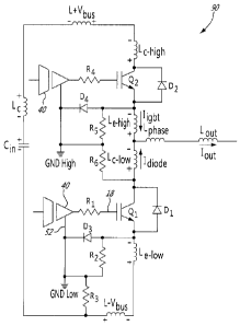
on
recovery current, with a very high di/dt. In this graph, the di/dt of the
current
400 through the freewheel diode 02 reaches over 6 kA/psec, exceeding the
manufacturer's recommendation of 5.5kA/psec. The voltage 410 across the
stray inductances of the high frequency loop is the mirror of the di/dt, i.e.
the
voltage across the IGBT, is below the bus voltage Vbõ, during the current
rise.
Without the present technology, the di/dt keeps increasing until the freewheel
diode spontaneously turns off. The dv/dt of the voltage 420 across the
CA 02907472 2015-09-17
WO 2014/161080
PCT/CA2014/000325
29
freewheel diode is very high and has significant oscillations 422 that cause
electromagnetic interference (EMI).
[00116] Figure 21 is a graphic illustrating recovery current of the
freewheel diode of Figure 19. By comparison with the graph of Figure 20, the
recovery current is controlled using the present technology. In this case,
di/dt
of the current 450 across the freewheel diode D2 is maintained within the
manufacturer recommendation of 5kA/psec when the diode turns off. In fact,
the di/dt is actually greater (steeper slope) at the beginning of the
transition,
but is timely reduced to the desired value to protect the device. The voltage
460 across the stray inductances of the high frequency loop reduces less
rapidly. The recovery current is lower when compared to Figure 20. The
voltage rise 470 is lower, and the oscillations 472 are reduced.
[00117] Experimental measurements were obtained in a laboratory,
under the same conditions, with and without the above described technology.
Figure 22 is a graphic illustrating a comparison of output currents as a
function
of bus voltages that can be provided with and without the circuit for limiting
turn-off overvoltage and turn-on recovery current. Figure 22 shows a
comparison of output currents that can be provided with an HP2 IGBT module
from lnfineonTM with a cooling liquid at 55 C and a hottest junction of all
the
dies at 130 C. Many drives, such as for example those developed for vehicular
applications, should resist any short-circuit condition. Usually, tests are
performed until the IGBT de-saturates. For the purpose of this experiment
leading whose results are shown on Figure 22, a maximum peak output
current of 2000 amperes was considered. The overvoltage was maintained
within 650 Vdc for all possible currents up to 2000 amperes. The gate drivers
were adjusted according to these requirements. For gate drivers without the
present technology, the on and off resistor values were adjusted.
[00118] Figure 22 illustrates root-mean-square (RMS) output currents
as a function of bus voltage. The operating frequency was 20 KHz, without any
modulation in both cases. The capability to provide the desired output current
CA 02907472 2015-09-17
WO 2014/161080
PCT/CA2014/000325
is affected by the operating voltage. Measurements were taken at voltages
ranging from 300 Vdc to 450 Vdc. Results using the gate driver without the
present technology (numeral 800) could only give half of the output current at
450 Vdc when compared to 300 Vdc. Results using the gate driver with the
present technology (numeral 802), on the other hand, could give more than
two thirds of the output current at 450 Vdc when compared to 300 Vdc. The
present technology not only helps to increase the output current for a same
given semiconductor configuration, but is also less sensitive to operating
voltages. On Figure 22, the slope of the output current loss with increasing
bus
voltage is lower with the present technology. This result therefore shows that
the present technology makes a commutation cell less dependent on the
switching losses.
[00119] Figure 23 is a graphic illustrating the output current as a
function of switching frequency using the circuit for limiting turn-off
overvoltage
and turn-on recovery current. The same experimental conditions used to
produce the results shown on Figure 22 were repeated when producing the
graph of Figure 23. A 300 Vdc bus voltage was maintained and the results are
provided as a function of the frequency. Using a logarithmic scale, with these
experimental measurements, it is expected that the HP2 IGBT module from
InfineonTm will be able to operate at 40 KHz and provide over 200 amperes.
[00120] The foregoing describes solutions applicable to DC-DC
converters and to DC-AC converters, for example commutation cells using a
full leg of semiconductors, opposite pairs of power electronic switches and
freewheel diodes, to provide alternative current to a connected load such as a
motor of an electric vehicle.
[00121] Those of ordinary skill in the art will realize that the
description
of the commutation cell and of the compensation circuit for limiting switching
overvoltage and for limiting recovery current are illustrative only and are
not
intended to be in any way limiting. Other embodiments will readily suggest
themselves to such persons with ordinary skill in the art having the benefit
of
CA 02907472 2015-09-17
WO 2014/161080
PCT/CA2014/000325
31
the present disclosure. Furthermore, the disclosed commutation cell and the
compensation circuit may be customized to offer valuable solutions to existing
needs and problems of overvoltage and recovery current occurring upon
switching in commutation cells.
[00122] In the interest of clarity, not all of the routine features of
the
implementations of commutation cell and of the compensation circuit are
shown and described. It will, of course, be appreciated that in the
development
of any such actual implementation of the commutation cell and of the
compensation circuit, numerous implementation-specific decisions may need
to be made in order to achieve the developer's specific goals, such as
compliance with application-, system-, and business-related constraints, and
that these specific goals will vary from one implementation to another and
from
one developer to another. Moreover, it will be appreciated that a development
effort might be complex and time-consuming, but would nevertheless be a
routine undertaking of engineering for those of ordinary skill in the field of
power electronics having the benefit of the present disclosure.
[00123] It is to be understood that the commutation cell and
compensation circuit for limiting switching overvoltage and for limiting
recovery
current is not limited in its application to the details of construction and
parts
illustrated in the accompanying drawings and described hereinabove. The
proposed commutation cell and compensation circuit for limiting switching
overvoltage and for limiting recovery current is capable of other embodiments
and of being practiced in various ways. It is also to be understood that the
phraseology or terminology used herein is for the purpose of description and
not limitation. Hence, although the commutation cell and compensation circuit
for limiting switching overvoltage and for limiting recovery current has been
described hereinabove by way of illustrative embodiments thereof, it can be
modified, without departing from the spirit, scope and nature of the subject
invention.