Note: Descriptions are shown in the official language in which they were submitted.
CA 2910385 2017-03-17
CONFORMAL ELECTRONICS INCLUDING NESTED SERPENTINE
INTERCONNECTS
BACKGROUND
[0002] High quality medical sensing and imaging data has become increasingly
beneficial in die diagnoses and treatment of a variety of medical conditions.
The
conditions can be associated with the digestive system, the cardio-circulatory
system,
and can include injuries to the nervous system, cancer, and the litre. To
date, most
electronic systems that could be used to gather such sensing or imaging data
have
been rigid and inflexible. These rigid electronics are not ideal for many
applications,
such as in biomedical devices. Most of biological tissue is soft and curved.
The skin
and organs are delicate and far from two-dimensional. Other potential
applications of
electronics systems, such as for gathering data in non-medical systems, also
can he
hampered by rigid electronics.
SUMMARY
[0003] Various examples described herein are directed generally to
methods,
apparatus, and systems that include interconnects that provide for greater
stretchability
and flexibility.
[0003a] According to the present invention, there is provided a stretchable
electrical
device, comprising:
two electrical contacts spaced apart by a distance; and
an electrical interconnect connected to and extending from a first one of the
two electrical contacts generally in a first direction and electrically
coupling the first one of the two electrical contacts with a second one of
the two electrical contacts;
wherein the electrical interconnect has a meander-shaped base
configuration comprising a plurality of repeated, connected, and
alternating loops, each of the plurality of loops having a curved tip and a
length extending from the curved tip in a second direction that is
generally perpendicular to the first direction, each of the lengths
1
CA 2910385 2017-03-17
connecting adjacent ones of the plurality of loops and each of the lengths
forming a nested serpentine-shaped feature projecting in the first
direction such that the electrical interconnect includes a plurality of
nested serpentine-shaped features arranged along the electrical
interconnect, each of the plurality of nested serpentine-shaped features
being at least partially nested within an adjacent one of the plurality of
nested serpentine-shaped features.
[0003b] According to the present invention, there is also provided a
stretchable
device, comprising:
a stretchable substrate; and
a stretchable electronic circuit disposed on a surface of the stretchable
substrate, the stretchable electronic circuit comprising:
a first discrete operative device;
a second discrete operative device spaced apart from the first discrete
operating device by a distance; and
a stretchable electrical interconnect connected to and extending from the
first discrete operating device generally in a first direction and
electrically coupling the first discrete operative device to the second
discrete operative device,
wherein the stretchable electrical interconnect has a meander-shaped
base configuration comprising a plurality of repeated, connected, and
alternating loops, each of the plurality of loops having a curved tip
and a length extending from the curved tip in a second direction that
is generally perpendicular to the first direction, each of the lengths
connecting adjacent ones of the plurality of loops and each of the
lengths forming a nested serpentine-shaped feature projecting in the
first direction such that the electrical interconnect includes a plurality
of nested serpentine-shaped features arranged along the electrical
interconnect, each of the plurality of nested serpentine-shaped
features being at least partially nested within an adjacent one of the
plurality of nested serpentine-shaped features.
la
CA 2910385 2017-03-17
[0003c] According to the present invention, there is also provided a
stretchable
electrical device, comprising:
two electrical contacts; and
an electrical interconnect electrically coupling the two electrical contacts;
wherein the electrical interconnect has a meander-shaped base configuration
comprising a plurality of nested serpentine-shaped features arranged
along the electrical interconnect such that each of the plurality of nested
serpentine-shaped features is at least partially nested within an adjacent
one of the plurality of nested serpentine-shaped features.
[0003d] According to the present invention, there is also provided a
stretchable
electrical device, comprising:
two electrical contacts spaced apart by a distance; and
an electrical interconnect connected to and extending from a first one of the
two electrical contacts generally in a first direction and electrically
coupling the first one of the two electrical contacts with a second one of
the two electrical contacts;
wherein the electrical interconnect has a meander-shaped base configuration
comprising a plurality of repeated, connected, and alternating loops,
each of the plurality of loops having a curved tip and a length extending
from the curved tip, wherein the plurality of loops includes (i) a first set
of curved tips generally disposed on a first side of the electrical
interconnect and (ii) a second set of curved tips generally disposed on a
second opposing side of the electrical interconnect, each of the lengths
forming a nested serpentine-shaped feature, each of the nested
serpentine-shaped features being disposed between the first side of the
electrical interconnect and the second side of the electrical interconnect
such that the electrical interconnect includes a plurality of nested
serpentine-shaped features arranged along the electrical interconnect,
each of the plurality of nested serpentine-shaped features being at least
partially nested within an adjacent one of the plurality of nested
serpentine-shaped features.
lb
CA 2910385 2017-03-17
[0003e] Preferred embodiments are described hereunder.
[0004] Example method, apparatus, and systems provide stretchable
electrical
devices that include two electrical contacts and an electrical interconnect
electrically
coupling the two electrical contacts.
[0005] According to an aspect, the example electrical interconnect can have
a meander-
shaped configuration that includes at least one nested serpentine-shaped
feature.
lc
CA 02910385 2015-10-26
WO 2014/186467
PCT/US2014/038002
Atty likt No.: MC10-037/01 WO 320609-2051
[00061 in an example implementation according to the first aspect, the
meander-shaped
configuration can be a serpentine structure, a zig-zag structure, a
boustrophedonic structure, a
rippled structure, a corrugated structure, or a helical structure.
[00071 According to an aspect, the example electrical interconnect can have
a serpentine-
in-serpentine configuration that includes a serpentine-shaped structure
including at least one
nested serpentine-shaped feature.
00081 The example two electrical contacts can be disposed on an elastomeric
substrate.
100091 in an example implementation, the stretchable electrical device can
be configured
such that two electrical contacts is in physical communication with the
elastomeric substrate,
and the electrical interconnect is not in physical communication with the
substrate.
[0010] In an example, at least one of the two electrical contacts can be in
communication
with a semiconductor circuit.
[00111 The example electrical contacts can be metal contacts.
[0012] In an example, the stretchable electrical device can include at
least one device
component in communication with at least one of the two electrical contacts.
The at least one
device componentcan be an electronic device component, an optical device
component, an
optoelectronic device component, a mechanical device component, a
microelectromechanical
device component, a nanoelectromechanical device component, a microfluidic
device
component or a thermal device.
[0013] Example methods, apparatus, and systems provide stretchable devices
that include
a stretchable substrate and a stretchable electronic circuit disposed on a
surface of the
stretchable substrate. The stretchable electronic circuit includes first and
second discrete
operative devices and a stretchable interconnect coupling the first discrete
operative device to
the second discrete operative device. The stretchable interconnect can have a
meander-
shaped configuration that includes at least one nested serpentine-shaped
feature.
[00141 According to different aspects, the meander-shaped configuration can
be a
serpentine structure, a zig-zag structure, a boustrophedonic structure, a
rippled structure, a
corrugated structure, or a helical structure.
100151 According to an aspect, the example stretchabe interconnect can have
a
serpentine-in-serpentine configuration.
2
106999529 vi
CA 2910385 2017-03-17
[0016] In an example, the first discrete operative device or the second
discrete operative
device can include a metal contact.
[0017] In an example, the first discrete operative device or the second
discrete operative
device is a semiconductor device.
[0018] The first and second discrete operative devices and the
stretchable interconnect
can be fabricated from the same material.
[0019] In an example, the same material can be a semiconductor material.
[0020] In an example, the stretchable interconnect can be made from a
semiconductor
material.
[0021] The first discrete operative device also can be formed from a
semiconductor
material. In an example, the stretchable interconnect is made from a different
semiconductor
material than the first discrete operative device.
[0022] In an example, the semiconductor material is a single crystal
semiconductor
material.
[0023] In an example implementation, the stretchable electrical device
can be
configured such that the first discrete operative device and the second
discrete operative
device are in physical communication with the surface of the stretchable
substrate, and the
stretchable interconnect is not in physical communication with the surface.
[0024] The first discrete, operative device or the second discrete
operative device can
include one or more of a photodetector, a photodiode array, a display, a light-
emitting
device, a photovoltaic device, a sensor array, a light-emitting diode, a
semiconductor laser,
an optical imaging system, a transistor, a microprocessor, an integrated
circuit, or any
combination of thereof
[0025] The following publications, patents, and patent applications arc
of interest:
[0026] Kim et al., "Stretchable and Foldable Silicon Integrated
Circuits," Science
Express, March 27, 2008, 10.1126/science, 1154367;
[0027] Ko et al., "A Hemispherical Electronic Eye Camera Based on
Compressible
Silicon Optoelectronics," Nature, August 7, 2008, vol. 454, pp. 748-753;
3
CA 02910385 2015-10-26
WO 2014/186467
PCT/US2014/038002
Atty Dkt No.: MC10-037/01 WO 320609-2051
[0028] Kim et al., "Complementary Metal Oxide Silicon Integrated Circuits
Incorporating Monolithically Integrated Stretchable Wavy Interconnects,"
Applied Physics
Letters, July 31, 2008, vol. 93, 044102;
[0029] Kim et al., "Materials and Noncoplanar Mesh Designs for Integrated
Circuits with
Linear Elastic Responses to Extreme Mechanical Deformations," PNAS, December
2, 2008,
vol. 105, no. 48, pp. 18675-18680;
[0030] Mei-a et al., "Transfer Printing by Kinetic Control of Adhesion to
an Elastomeric
Stamp," Nature Materials, January, 2006, vol. 5, pp. 33-38;
[0031] U.S. Patent Application publication no. 2010 0002402-Al, published
January. 7,
2010, filed March 5, 2009, and entitled "STRETCHABLE AND FOLDABLE
ELECTRONIC DEVICES;"
10032] U.S. Patent Application publication no. 2010 0087782-AI, published
April 8,
2010, filed October 7, 2009, and entitled "CATHETER BALLOON HAVING
STRETCHABLE INTEGRATED CIRCUITRY AND SENSOR ARRAY;"
[00331 U.S. Patent Application publication no. 2010 0116526-Al, published
May 13,
2010, filed November .12, 2009, and entitled "EXTREMELY STRETCHABLE
ELECTRONICS;"
100341 U.S. Patent Application publication no. 2010 0178722-Al, published
July 15,
2010, filed January 12, 2010, and entitled "METHODS AND APPLICATIONS OF NON-
PLANAR IMAGING ARRAYS;" and
[0035] U.S. Patent Application publication no. 2010 027119-Al, published
October 28,
2010, filed November 24, 2009, and entitled "SYSTEMS, DEVICES, AND METHODS
UTILIZING STRETCHABLE ELECTRONICS TO MEASURE TIRE OR ROAD
SURFACE CONDITIONS."
[0036] Kim, D. H. et al. (2010). Dissolvable films of silk fibroin for
uhrailtin conformal
bin-integrated electronics. Nature Materials, 9, 511---517.
100371 Omenetto, F.G. and D. L. Kaplan, (2008). A new route for silk,
Nature Photonics,
2,641-643.
100381 Omenetto, F. 0., Kaplan, D. L. (2010). New opportunities for an
ancient material.
Science, 329, 528 -531.
4
106999529 vi
CA 02910385 2015-10-26
WO 2014/186467
PCT/US2014/038002
Atty Dkt No.: MC10-037/01 WO 320609-2051
[0039] Halsed, W. S. (1913). Ligature and suture material. Journal of the
American
Medical Association, 60, 1119 -1126.
100401 Masuhiro, T., Yoko, G., Masaobu, N. etal. (1994). Structural changes
of silk
fibroin membranes induced by immersion in methanol aqueous solutions. Journal
of Polymer
Science, 5, 961---968.
[0041] Lawrence, B. D., Cronin-Golomb, M., Georgakoudi, I., et al. (2008).
Bioactive
silk protein biomaterial systems for optical devices. Biomacromolecules, 9,
1214-1220.
[0042] Demura, M., Asakura, T. (1989). Immobilization of glucose oxidase
with Bombyx
mon silk fibroin by only stretching treatment and its application to glucose
sensor.
Biotechnololgy and Bioengineering, 33, 598-603.
[0043] Wang, X., Zhartg, X., Castellot, J. et al. (2008).Controlled release
from multdayer
silk biomaterial coatings to modulate vascular cell responses. Biomaterials,
29, 894---903.
[0044] U.S. Patent Application Serial No. 12/723,475 entitled "SYSTEMS,
METHODS,
AND DEVICES FOR SENSING AND TREATMENT HAVING STRETCHABLE
INTEGRATED CIRCUITRY," filed March 12, 2010.
[0045] -U.S. Patent Application Serial No. 12/686,076 entitled "Methods and
Applications
of Non-Planar Imaging Arrays," filed January 12, 2010.
[0046] U.S. Patent Application Serial No. 12/636,071 entitled "Systems,
Methods, and
Devices Using Stretchable or Flexible Electronics for Medical Applications,"
filed December
11, 2009.
[0047] -U.S. Patent Application publication no 2012-0065937-Al, published
March 15,
2012, and entitled "METHODS AND APPARATUS FOR MEASURING TECHNICAL
PARAMETERS OF EQUIPMENT, TOOLS AND COMPONENTS VIA CONFORMAL
ELECTRONICS."
[00481 U.S. Patent Application Serial No. 12/616,922 entitled "Extremely
Stretchable
Electronics," filed November 12, 2009,
100491 U.S. Patent Application Serial No. 12/575,008 entitled "Catheter
Balloon Having
Stretchable Integrated Circuitry and Sensor Array," filed on October 7, 2009.
106999529 vi
CA 2910385 2017-03-17
[0050] U.S. Patent Application Serial No. 13/336,518 entitled "Systems,
Methods, and
Devices Having, Stretchable Integrated Circuitry for Sensing and Delivering,
Therapy," filed
December 23, 2011.
[0051] U.S. Patent Application Serial No. 13/843,873 entitled "STRAIN
ISOLATION
STRUCTURES FOR STRETCHABLE ELECTRONICS," filed March 15, 2013.
[0052] U.S. Patent Application Serial No. 13/843,880 entitled "STRAIN
RELIEF
STRUCTURES FOR STRETCHABLE INTERCONNECTS," filed March 15, 2013.
[0053] It should be appreciated that all combinations of the foregoing
concepts and
additional concepts described in greater detail below (provided such concepts
are not
mutually inconsistent) are contemplated as being part of the inventive subject
matter
disclosed herein. It also should be appreciated that terminology explicitly
employed herein
should be accorded a meaning, most consistent with the particular concepts
disclosed herein,
BRIEF DESCRIPTION OF THE DRAWPNQS
[0054] The skilled artisan will understand that the figures, described
herein, are for
illustration purposes only, and that the drawings are not intended to limit
the scope of the
disclosed teachings in any way. In some instances, various aspects or features
may be shown
exaggerated or enlarged to facilitate an understanding of the inventive
concepts disclosed
herein (the drawings are not necessarily to scale, emphasis instead being
placed upon
illustrating the principles of the teachings). In the drawings, like reference
characters
generally refer to like features, functionally similar and/or structurally
similar elements
throughout the various figures.
[0055] FIG. 1A shows an example stretchable device according to the
principles
described herein.
100561 FIG. 1B shows an example of the composite configurations of the
example
interconnect of FIG. 1A, according to the principles described herein.
[0057] FIG. 2 shows an example of the deformation of an interconnect
according to the
principles described herein.
[0058] FIG. 3 is an example stretchable device according to the
principles described
herein.
6
CA 02910385 2015-10-26
WO 2014/186467
PCT/US2014/038002
Atty Dkt No.: MC10-037/01 WO 320609-2051
[0059] FIG. 4A shows another example stretchable device according to the
principles
described herein.
[0060] FIG. 4B shows an example of the composite configurations of the
example
interconnect of FIG-. 4A, according to the principles described herein.
[0061] FIG. 5 shows an. example stretchable device according to the
principles described
herein.
[0062] FIG. 6 shows an example stretchable device according to the
principles described
herein.
[00631 FIG. 7 shows an example stretchable device according to the
principles described
herein.
[0064] FIG. 8 shows an example stretchable device according to the
principles described
herein.
[0065] FIGs. 9A and 9B show other example interconnects according to the
principles
described herein.
[0066] EEGs. 1.0A and I OB show examples of shaped of serpentine-shaped
features
according to the principles described herein.
[0067] FICis. 11A - IIC shows ex.amples of interconnects according to the
principles
described herein.
[0068] FIG. 12 shows an example stretchable device according to the
principles described
herein.
[0069] Fla 13A. shows an example configuration of interconnects and device
islands
according to the principles described herein.
[0070] FIG. 13B shows an example cross-section of a portion of the
interconnects and
device islands of FIG. 13A according to the principles described herein.
[0071] FIG. 14 shows an example stretchable device according to the
principles
described herein.
[0072] FIGs 15A-15D show example device configurations according -to the
principles
described herein.
7
106999529 vi
CA 02910385 2015-10-26
WO 2014/186467
PCT/US2014/038002
Atty likt No.: MC10-037/01 WO 320609-2051
[00731 Pith. 16A-16C show example system configurations according to the
principles
described herein.
100741 FIG. 17 shows the architecture of an example computer system
according to the
principles described herein.
100751 FIG. 18 shows an example conformal sensor device according to the
principles
described herein.
DETAILED DESCRIPTION
100761 Following below are more detailed descriptions of various concepts
related to, and
embodiments of, inventive methods, apparatus and systems for monitoring
hydration via
conformal electronics. It should be appreciated that various concepts
introduced above and
discussed in greater detail below may be implemented in any of numerous ways,
as the
disclosed concepts are not limited to any particular manner of implementation.
Examples of
specific implementations and applications are provided primarily for
illustrative purposes.
[00771 As used herein, the term "includes" means includes but is not
limited to, the term
"including" means including but not limited to. The term "based on" means
based at least in
part on.
[00781 With respect to substrates or other surfaces described herein in
connection with
various examples of the principles herein, any references to "top" surface and
"bottom"
surface are used primarily to indicate relative position, alignment andlor
orientation of
various elements/components with respect to the substrate and each other, and
these terms do
not necessarily indicate any particular frame of reference (e.g., a
gravitational frame of
reference). Thus, reference to a "bottom" of a substrate or a layer does not
necessarily
require that the indicated surface or layer be facing a ground surface.
Similarly, terms such
as "over," "under," "above," "beneath" and the like do not necessarily
indicate any particular
frame of reference, such as a gravitational frame of reference, but rather are
used primarily to
indicate relative position, alignment and/or orientation of various
elements/components with
respect to the substrate (or other surface) and each other. The terms
"disposed on" "disposed
in" and "disposed over" encompass the meaning of "embedded in," including
"partially
embedded in." In addition, reference to feature A being "disposed on,"
"disposed between,"
or "disposed over" feature B encompasses examples where feature A is in
contact with
feature B, as well as examples where other layers and/or other components are
positioned
between feature A and feature B.
8
106999529 vi
CA 02910385 2015-10-26
WO 2014/186467
PCT/US2014/038002
Atty likt No.: MC10-037/01 WO 320609-2051
[00791 Example systems, apparatus and methods described herein provide
conformal
electronics that present greater stretchability and flexibility than existing
devices due to
implementation of an example interconnect according to the principles
described herein. In
an example, the conformal electronics can be formed as stretchable electrical
devices that
include electrical contacts and at least one electrical interconnect
electrically coupling the
electrical contacts. hi an example, the conformal electronics can be formed as
stretchable
devices that include a stretchable substrate and a stretchable electronic
circuit disposed on a
surface of the stretchable substrate. As a non-limiting example, the
stretchable electronic
circuit can include at least one discrete operative device and a stretchable
interconnect
coupled to the at least one discrete operative device. For example, the
stretchable
interconnect according to the principles herein can be implemented to couple a
first discrete
operative device to a second discrete operative device.
[00801 In any example herein, the example interconnect can be configured as
a fractal
serpentine interconnect.
100811 In one non-limiting example implementation, the fractal serpentine
interconnect
can be configured to have a meander-shaped configuration that includes at
least one nested
serpentine-shaped feature.
[00821 In another the electrical interconnect non-limiting example
implementation, the
fractal serpentine interconnect can be configured to have a serpentine-in-
serpentine ("Sir)
configuration that includes a serpentine-shaped structure including at least
one nested
serpentine-shaped feature.
[00831 Any example fractal serpentine interconnect according to the
principles herein can
be formed as an electrically conductive interconnect. In other examples, the
example fractal
serpentine interconnect can be formed as a thermally conductive interconnect,
or as a non-
conductive interconnect formed from an electrically non-conductive material.
[00841 In any example implementation, a fractal serpentine interconnect
according to the
principles herein can be flinned as bi-axial, extremely stretchable, high fill-
factor
interconnects. An example fractal serpentine interconnect can be configured as
"fractal"
serpentine structures built into a "base" overall meander-shaped structure
(including a
serpentine structure). In an example, the example fractal serpentine
structures can be
configured as a nested serpentine feature. An example fractal serpentine
interconnect can be
configured in such a way that the fractal features have multiple wavelengths,
amplitudes, and
9
106999529 vi
CA 02910385 2015-10-26
WO 2014/186467
PCT/US2014/038002
Atty likt No.: MC10-037/01 WO 320609-2051
are positioned in locations that allow the base serpentine interconnect or
meander-shaped
structure to be stretched in multiple directions, such as, e.g., the
transversal direction. Due to
the fractal serpentine design, the overall length of the interconnects
according to the
principles described herein (also referred to as fractal serpentine
interconnects) is greater than
that of other existing serpentine or meander-shaped structures. That is, if a
fractal serpentine
interconnect according to the principles herein were stretched and extended to
the full length,
the fractal serpentine interconnect would be longer in length than an
interconnect having a
solely meander shape (including a serpentine shape). Thus, the fractal
serpentine
interconnect configuration facilitates fitting a longer length of interconnect
into effectively
the same stretchable area. Thus, the fractal serpentine interconnect
configurations according
to the principles described herein present high fill factors and are extremely
stretchable and
flexible.
[00851 In example implementations, apparatus according to the principles
described
herein include devices based on conformal (e.g., stretchable, flexible and/or
bendable)
electronics that include the fractal serpentine interconnects.
[00861 In an example, the fractal serpentine interconnects can be formed
from a
conductive material or from a non-conductive material.
[00871 In an example, a system, apparatus and method is provided that is
based on thin
device islands, including integrated circuitry (IC) chips and/or stretchable
interconnects that
are embedded in a flexible polymer.
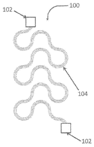
[00881 FIG. 1A. shows an example stretchable device according to the
principles
described herein. The example stretchable device 100 includes contacts 102 and
at least one
interconnect 154 coupled to the contacts 102. In an example, contacts 102 can
be electrical
contacts, and the interconnect 154 can be an electrical interconnect that
electrically couples
the electrical contacts. In this example, the example interconnect 154 has a
meander-shaped
configuration that includes at least one nested serpentine-shaped feature.
[00891 FIG. I B shows the composite configurations of the interconnect 154
of FIG. IA.
Interconnect 154 is comprised of a meander-shaped configuration 152 that
includes several
nested serpentine-shaped features 154. In this example, each nested serpentine-
shaped
features 154 is disposed at a portion 156 of each repeat loop of the meander-
shaped
configuration 152. In other examples, the nested serpentine-shaped feature 154
may be
disposed at different portions of the meander-shaped configuration 152, such
as but not
106999529 vi
CA 02910385 2015-10-26
WO 2014/186467
PCT/US2014/038002
Atty Dkt No.: MC10-037/01 WO 320609-2051
limited to, at a tip 158 of a loop of the meander-shaped configuration 152. in
other examples,
the nested serpentine-shaped feature 154 may be disposed both at a position
along a length of
a loop (such as position 156) and at a tip of a loop (such as position 158).
In some examples,
the nested serpentine-shaped features 154 of an interconnect 154 may be
configured with
multiple differing wavelengths (1,) and/or differing amplitudes (a).
[00901 FIG. 2 shows an example of the stretching direction and expansion
directions of
an example fractal serpentine interconnect. Any example interconnect described
herein can
be subjected to several different directions of deformation. According to the
principles
herein, the nested serpentine-shaped features are disposed at portions of the
meander-shaped
configuration such that the interconnect can be stretched in a bi-axial
direction or multiple
directions, such as but not limited to a transversal direction.
100911 FIG. 3 shows another example stretchable device according to the
principles
described herein. The example stretchable device 300 includes contacts 302 and
at least One
interconnect 304 coupled to the contacts 302. In an example, contacts 302 can
be electrical
contacts, and the interconnect 304 can be an electrical interconnect that
electrically couples
the electrical contacts. In this example, the example interconnect 304 has a
meander-shaped
configuration 352 that includes several nested serpentine-shaped features 354.
The nested
serpentine-shaped features 354 are disposed at regions along each repeat loop
of the
meander-shaped configuration 352. In some examples, the nested serpentine-
shaped features
354 of an interconnect 304 may be configured with in ult ip I e differing
wavelengths and/or
differing amplitudes.
100921 FIG. 4A. shows another example stretchable device according to the
principles
described herein. The example stretchable device 400 includes contacts 402 and
at least one
interconnect 404 coupled to the contacts 402. In an example, contacts 402 can
be electrical
contacts, and the interconnect 404 can be an electrical interconnect that
electrically couples
the electrical contacts. FIG. 4B shows the composite configurations of the
interconnect 404
of FIG. 4A, Example interconnect 404 has a meander-shaped configuration 452
that includes
several nested serpentine-shaped features 454. The nested serpentine-shaped
features 454 are
disposed at regions along each repeat loop of the meander-shaped configuration
452. in other
examples, the nested serpentine-shaped feature 454 may be disposed at
different portions of
the meander-shaped configuration 452, such as but not limited to, at a tip 458
of a loop of the
meander-shaped configuration 452. In other examples, the nested serpentine-
shaped feature
454 may be disposed both at a position along a length of a loop and at a tip
of a loop (such as
106999529 vi
CA 02910385 2015-10-26
WO 2014/186467
PCT/US2014/038002
Atty Dkt No.: MC10-037/01W0 320609-2051
position 458). In some examples, the nested serpentine-shaped features 454 of
an
interconnect 404 may be configured with multiple differing wavelengths and/or
differing
amplitudes.
[0093] FIGs. 5 and 6 show other example stretchable devices according to
the principles
described herein that include interconnects having a meander-shaped
configuration including
at least one nested serpentine-shaped feature. In the examples of FIGs. 5 and
6, the meander-
shaped configuration is serpentine-shaped, such that the interconnect has a
serpentine-in-
serpentine (SiS) configuration. The example stretchable device of FIG. 5
includes contacts
502 and at least one interconnect 504 coupled to the contacts 502. Example
interconnect 504
has a serpentine-shaped structure 552 that includes several nested serpentine-
shaped features
554. The nested serpentine-shaped features 554 are disposed at the tips of
each repeat loop of
the serpentine-shaped structure 552. In this example, the nested serpentine-
shaped features
554 are oriented towards the midpoint of each loop. The example stretchable
device of FIG.
6 includes contacts 602 and at least one interconnect 604 coupled to the
contacts 602.
Example interconnect 604 has a serpentine-shaped structure 652 that includes
several nested
serpentine-shaped features 654. The nested serpentine-shaped features 654 are
disposed at
the tips of each repeat loop of the serpentine-shaped structure 652. In this
example, the
nested serpentine-shaped features 654 are oriented outwards from each loop.
[0094] Example contacts 502 and 602 can. be configured as electrical
contacts, and the
interconnects 504 and 604 can be electrical interconnects that electrically
couples the
respective electrical contacts. In some examples, the nested serpentine-shaped
feature 554 or
654 may be disposed at different portions of the serpentine-shaped structure
552 or 652, such
as but not limited to, along a portion of a length of a loop. in other
examples, the nested
serpentine-shaped feature 554 or 654 may be disposed both at a position along
a length of a
loop and at a tip of a loop. In some examples, the nested serpentine-shaped
features 554 and
654 of an interconnect 504 and 604, respectively, may be configured with
multiple differing
wavelengths and/or differing amplitudes.
[0095] FIG6. 7 and 8 show other example stretchable devices according to
the principles
described herein that include interconnects having a meander-shaped
configuration including
nested serpentine-shaped features. The example stretchable device of FIG. 7
includes
contacts 702 mid at least one interconnect 704 coupled to the contacts 702.
Example
interconnect 704 has a meander-shaped configuration 752 that includes several
nested
serpentine-shaped features 754. The example stretchable device of FIG. 8
includes contacts
12
106999529 vi
CA 02910385 2015-10-26
WO 2014/186467
PCT/US2014/038002
Atty likt No.: MC10-037/01 WO 320609-2051
802 and at least one interconnect 804 coupled to the contacts 802. Example
interconnect 804
has a meander-shaped configuration 852 that includes several nested serpentine-
shaped
features 854-a and 854-b. The nested serpentine-shaped features 854-a are
disposed along a
length of each repeat loop of the meander-shaped configuration 852, while
nested serpentine-
shaped features 854-b are disposed at the tips of each repeat loop of the
meander-shaped
configuration 852. Example contacts 702 and 702 can be configured as
electrical contacts,
and the interconnects 704 and 804 can be electrical interconnects that
electrically couples the
respective electrical contacts. In some examples, the nested serpentine-shaped
feature 754 or
854 may be disposed at different portions of the serpentine-shaped structure
752 or 852, such
as but not limited to, along a portion of a length of a loop. In other
examples, the nested
serpentine-shaped feature 754 or 854 may be disposed both at a position along
a length of a
loop and at a tip of a loop. In some examples, the nested serpentine-shaped
features 754 and
854 interconnect 704 and 804, respectively, may be configured with multiple
differing
wavelengths and/or differing amplitudes.
100961 FIGs. 9A and 9B show other example interconnects that can be
implemented
based on differing types of meander-shaped configurations, according to the
principles
described herein. In the example of FIG. 9A, the meander-shaped configuration
is a
boustrophedonic-shaped structure. The example stretchable device of FIG. 9A
includes
contacts 902 and an interconnect 904 coupled to the contacts 902, where the
example
interconnect 904 has a boustrophedonic-shaped structure that includes at least
one nested
serpentine-shaped feature 954. In the example of FIG. 9B, the meander-shaped
configuration
is a zig-zag-shaped structure. The example stretchable device of FIG. 9B
includes contacts
912 and an interconnect 914 coupled to the contacts 912, where the example
interconnect 914
has a zig-zag-shaped structure that includes at least one nested serpentine-
shaped feature 954.
100971 In other examples, the interconnect can have any other meander-
shaped
configuration in the art. For example, the meander-shaped configuration can be
configured to
have any number of linear or non-linear structure, including a corrugated or
rippled structure,
a helical structure, or any other configuration of that provides a flexible
and/or stretchable
interconnect.
[00981 FIGs. 10A and 10B show other non-limiting examples of serpentine
shapes that
the can be implemented as nested serpentine-shaped features, according to the
principles
described herein. As shown in FIGs. 10A and 10B, the nested serpentine-shaped
feature can
be modeled as a series of circular arcs. The turning angle of the arcs in the
example of FIG.
13
106999529 vi
CA 02910385 2015-10-26
WO 2014/186467
PCT/US2014/038002
Atty Dkt No.: MC10-037/01 WO 320609-2051
10A are smaller than the turning angle of the arcs in the example of FIG. 10B.
Therefore, the
arcs of the example serpentine structure of FIG. 10B are inure circular than
the arcs of the
example serpentine structure of FIG. 10A.
[0099] In any example implementation, a stretchable device can include
electrical
contacts and at least one interconnect disposed on a flexible and/or
stretchable substrate. In
an example, the flexible and/or stretchable substrate can be an elastomeric
substrate. In an
example, the electrical contacts can be in physical communication with the
surface of the
flexible and/or stretchable substrate and the interconnect is not in physical
communication
with the flexible and/or stretchable substrate.
[001001 In any example implementation, the electrical contacts can be in
communication
with a semiconductor circuit.
[001011 in any example implementation, the electrical contacts can he in
communication
with at least one device component in communication with at least one
electrical contact, and
wherein the at least one device component is an electronic device component,
an optical
device component, an optoelectronic device component, a mechanical device
component, a
microelectromechanical device component, a nanoelectromechanical device
component, a
mierofluddie device component or a thermal device.
[00102/ In any of the examples described herein, the electrically conductive
material (such
as but not limited to the material of the electrical interconnect and/or the
electrical contact)
can be, but is not limited to, a metal, a metal alloy, a conductive polymer,
or other conductive
material. In an example, the metal or metal alloy of the coating may include
but is not
limited to aluminum, stainless steel, or a transition metal, and any
applicable metal alloy,
including alloys with carbon_ examples of the transition metal include
copper,
silver, gold, platinum, zinc, nickel, titanium, chromium, or palladium, or any
combination
thereof. In other non-limiting examples, suitable conductive materials may
include a
semiconductor-based conductive material, including a silicon-based conductive
material,
indium tin oxide or other transparent conductive oxide, or Group III-1V
conductor (including
GaAs). 'The semiconductor-based conductive material may be doped.
[001031 in ally of the example structures described herein, the
interconnects can have a
thickness of about 0.1 pin, about 0.3 gm, about 0.5 gm, about 0.8 pm, about I
grn, about 1.5
um, about 2 gm, about 5 p.m, about 9 ttm, about 12 p.m, about 25 p.m, about 50
m, about 75
gm, about 100 gm, or greater.
14
106999529 vi
CA 02910385 2015-10-26
WO 2014/186467
PCT/US2014/038002
Atty Dkt No.: MC10-037/01W0 320609-2051
[Hi 041 In an example system, apparatus and method, the interconnects can be
formed
from a non-conductive material and can be used to provide some mechanical
stability and/or
mechanical stretchability between. components of the conformal electronics
(e.g., between
device components). As a non-limiting example, the non-conductive material
can. he formed
based on a polyimide.
[00105] in any of the example devices according to the principles described
herein, the
non-conductive material (such as but not limited to the material of a
stretchable interconnect)
can be formed from any material having elastic properties. For example, the
non-conductive
material can be formed from a polymer or polymeric material. Non-limiting
examples of
applicable polymers or polymeric materials include, but are not limited to, a
polyimide,
polyethylene terephthalate (PET), a silicone, or a polyeurethane. Other non-
limiting
examples of applicable polymers or polymeric materials include plastics,
elastomers,
thermoplastic elastomers, elastoplastics, thermostats, thermoplastics,
acrylates, acetal
polymers, biodegradable polymers, cellulosic polymers, fluoropolym.ers,
nylons,
polya.crylonitrile polymers, polyamide-imide polymers, polyarylates,
polybenzimidazole,
polybutylene, polycarbonate, polyesters, polyetherimide, polyethylene,
polyethylene
copolymers and modified polyethylenes, polyketones, poly(methyl methacrylate,
polymethylpentene, polyphenylene oxides and polyphenylene sulfides,
polyphlhalamide,
polypropylene, polyurethanes, styrenic resins, sulphone based resins, vinyl-
based resins, or
any combinations of these materials. In an example, a polymer or polymeric
material herein
can be a DYMAX0 polymer (Dymax Corporation , Torrington, CT).or other UV
curable
polymer, or a silicone such as but not limited to ECOFLEX (BASF, Florhatn
Park, NJ).
li)01061 in any example herein, the non-conductive material can have a
thickness of about
0.1 gm, about 0.3 p.m, about 0.5 p.m, about 0.8 um, about I pm, about 1.5 gm,
about 2 gm or
greater. in other examples herein, the non-conductive material can have a
thickness of about
I 0 um, about 20 p.m, about 25 pm, about 50 pm, about 75 pm, about 100 um,
about 125 pm,
about 150 pm, about 200 Km or greater.
[00107] In an example system, apparatus and method, the interconnects can be
formed
from an electrically conductive material that is covered or coated at least in
part by a non-
conductive material. In an example implementation where the conductive
interconnect
includes a coating of a non-conductive material, the dimensions of the
interconnects can be
defined based on the thickness of the conductive portion of the interconnect
versus the
thickness of the non-conductive coating material, also referred to as the
"trace and space".
106999529 vi
CA 02910385 2015-10-26
WO 2014/186467
PCT/US2014/038002
Atty likt No.: MC10-037/01 WO 320609-2051
FIGs. II A¨ IIC shows variations of the top-view cross-sections of
interconnects including a
conductive portion 1102, 1122, 1142 and a non-conductive coating 1100, 1120,
1140. In the
examples of FIGs. I IA and II C, the conductive portion and the non-conductive
portion have
approximately the same width. In the example of FM. 1113, the non-conductive
portion has a
greater width than the conductive portion.
[001081 In an example implementation illustrated in FIGs. 1 IA I IC, notation
"x" can
represent a dimension of about 75 um and notation "y" can represent a
dimension of about 25
um. In an example, the dimensions of FIG. 11A can be used where the thickness
of the
conductive portion is about 5 gm to about 181un thick. When the thickness of
conductive
portion is increased, the thickness of the non-conductive portion may be
reduced to maintain
the same interconnect thickness.
[001091 Non-limiting example processes that can be used for generating the
interconnects
include an etching process, a metal deposition process, or other wafer-based
fabrication
process. A metal deposition process may be used to provide interconnects with
greater
thicknesses. A wafer-based process may be used to provide interconnects with
finer lateral
features. In this example, any interconnect or other structure made using a
wafer-based
fabrication process may be released from the wafer substrate prior to further
processing.
[001101 In an example system, apparatus and method, sensors and other
electronics are
described herein that can include one or more of any of the fractal serpentine
interconnects
according to the principles described herein.
[0011.11 In an example system, apparatus and method, the interconnects can
be formed
from an electrically and/or thermally conductive material and can be used to
provide
electrical and/or thermal communication between components of the conformal
electronics,
e.g., between discrete operative device components. In any of the example
devices according
to the principles described herein, at least a portion of an example
interconnect can be formed
from an electrically conductive material.
[001121 An example stretchable device according to the principles described
herein can
include an example stretchable and/or flexible substrate, and an example
stretchable
electronic circuit disposed on a surface of the stretchable and/or flexible
substrate. In an
example, the stretchable electronic circuit can include at least one discrete
operative device
coupled to a stretchable interconnect that has a meander-shaped configuration
including at
least one nested serpentine-shaped feature. For example, the stretchable
electronic circuit can
16
106999529 vi
CA 02910385 2015-10-26
WO 2014/186467
PCT/US2014/038002
Atty likt No.: MC10-037/01 WO 320609-2051
include two discrete operative devices and a stretchable interconnect coupled
to the discrete
operative devices, where the stretchable interconnect has a meander-shaped
configuration
including at least one nested serpentine-shaped feature.
[001131 FIG. 12 shows an example stretchable device 1200 that includes an
example
stretchable and/or flexible substrate 1202, and an example stretchable
electronic circuit
disposed on a surface of the stretchable and/or flexible substrate 1202. In an
example, the
stretchable electronic circuit includes two discrete operative devices 1204,
1206 and a
stretchable interconnect 1208 coupled to the discrete operative devices 1204,
1206. As
shown in FIG. 12, the stretchable interconnect can have a meander-shaped
configuration
1222 including at least one nested serpentine-shaped feature 1224. In
different examples, the
stretchable interconnect can be any interconnect according to any of the
principles described
herein, including the interconnect of any of FIGs. IA through 10. The
description of material
composition, dimensions, and properties of any interconnect described herein,
including the
interconnects of any of FIGs. IA through 10, apply to the stretchable
interconnect of 1208.
100114j In any example implementation, one or more of the discrete operative
devices can
include a metal contact. The stretchable interconnect can be electrically
coupled to the
contact.
[001151 In any example implementation, the stretchable interconnect and one or
more of
the discrete operative devices can be fabricated from the same material, such
as but not
limited to a semiconductor material.
1.001161 In any example implementation, the stretchable interconnect can be
made from a
semiconductor material. The discrete operative device is formed from a
different
semiconductor material than the stretchable interconnect.
[001171 In any example implementation, the stretchable interconnect can be
made from a
single crystal semiconductor material.
1.001181 In any example implementation, the one or more discrete operative
devices can be
in physical communication with the surface of a stretchable and/or flexible
substrate, and the
stretchable interconnect is not in physical communication with the surface of
the flexible
and/or stretchable substrate.
[001191 In any example herein, the discrete operative device can be a
semiconductor
device. For example, the discrete operative device can be one or more of an
electronic
device, an optical device, an opto-electronic device, a mechanical device, a
17
106999529 vi
CA 02910385 2015-10-26
WO 2014/186467
PCT/US2014/038002
Atty likt No.: MC10-037/01 WO 320609-2051
microelectrornechanical device, a nanoelectromechanical device, a microfluidic
device, a
sensor, a light-emitting device, or a thermal device.
[001201 For example, the discrete operative device can include one or more of
a
photodetector, a photodiode array, a display, a light-emitting device, a
photovoltaic device, a
sensor array, a light-emitting diode, a semiconductor laser, an optical
imaging system, a
transistor, a microprocessor, an integrated circuit, or any combination of
thereof.
[00121] In an example, a conformal electronic structure is provided that
includes a -fractal
serpentine interconnect in electrical communication with at least one device
component. The
fractal serpentine interconnects and at least one device component can be
disposed on a
portion of a supporting surface of a flexible and/or a stretchable substrate.
[001221 In a non-limiting example, the flexible substrate can be a polymer.
For example,
the flexible substrate can be, but is not limited to, an elastomer, a
polyimide, a foil, paper,
fabric, or other flexible material. In another example, the flexible substrate
can be a
stretchable substrate.
[001231 In another example, a conformal electronic structure is provided that
includes at
least one device component and at least two fractal serpentine interconnects,
each of the at
least two fractal serpentine interconnects being in electrical communication
with the at least
one device component.
1001241 In an example system, apparatus and method herein, a fully conformal
electronic
device is provided that includes one or more of the fractal serpentine
interconnects. The frilly
conformal electronic device can be placed on, including being attached on, a
variety of
surface profiles, with minimal to no effect on the functionality of the
conformal electronic
device sensor. As a non-limiting example, the conformal device can be a
sensor.
[00125] In an example, a stretchable device according to the principles
described herein
can be configured as a sensor. A portion of the example sensor can be formed
with a fractal
serpentine interconnect that maintains mechanical stability during deformation
and/or
stretching of the sensor. For example, the fractal serpentine interconnect can
be formed at
least in part from a non-conductive material that is stretchable. Components
of the example
sensors can be linked by one or more of the fractal serpentine interconnect to
provide the
mechanical stability during deformation and/or stretching of the sensor.
[00126] In a non-limiting example, a stretchable device according to the
principles
described herein can be formed as a two-dimensional device. The discrete
operative device
18
106999529 vi
CA 02910385 2015-10-26
WO 2014/186467
PCT/US2014/038002
Atty Dkt No.: MC10-037/01 WO 320609-2051
components can include one or more materials such as a metal, a semiconductor,
an insulator,
a piezoelectric material, a ferroelectric material, a magnetostrictive
material, an
electrostrictive material, a superconductor, a ferromagnetic material, or a
thermoelectric
m ateri a
[001271 in a non-limiting example stretchable device, at least one of the
discrete operative
components can be disposed on a device island, with the interconnect being
coupled to the
discrete operative component via the device island. FIGs. 13A 13B show an
example of a
configuration of interconnects disposed between, and coupled to, spaced apart
device islands.
As shown in FIG. 1.3A, the stretchable device can. include a plurality of
device islands 1302
arranged co-planar plane relative to each other, each of the device islands
including one or
more discrete operative device components 1304. A plurality of interconnects
1306 can he
used to couple adjacent device islands, or to couple conductive contacts to
device islands.
While the example of FIG. 13A shows serpentine-shaped interconnects, one or
more of the
interconnects 1306 can be configured as a meander-shaped configuration
including at least
one nested serpentine-shaped feature according to the principles described
herein_ The
resulting example stretchable device would have significantly greater
flexibility,
stretchability, and robustness to multi-axial deformations based on th.e
greater stretchability
of the fractal serpentine interconnect. In the example of FIG. 13A, two
interconnects 1306
are used to couple device islands in each row or to couple contacts to the
device islands; at
least one interconnect 1306 couples adjacent device islands across the two
rows.
[0012N] in other example implementations, the device islands and/or the
interconnects can
be disposed in a three-dimensional arrangement. For example, the device
islands and/or the
interconnects the interconnects can be arranged in a single layer or in
multiple layers (e.g.,
two or more layers). In an example, two or more interconnects between device
islands can be
disposed in a co-planar, substantially parallel arranaement Any multiple-
layered portion of
an example structure can be arranged in a staggered arrangement, a stacking
arrangement, or
a randomized arrangement. That is, the interconnects can be multiple layer
stacking, or can.
be placed in a coplanar parallel arrangement. In various examples, the
components can be
oriented in differing directions in each stacked layer, and/or each layer of
the stacked layers
can include differing numbers of device islands or interconnects. in other
examples, at least a
portion of the device islands and the interconnects of a structure can be
disposed in a
substantially curved arrangement.
19
106999529 vi
CA 02910385 2015-10-26
WO 2014/186467
PCT/US2014/038002
Atty likt No.: MC10-037/01 WO 320609-2051
[001291 FIG. 13B shows a cross-section through line "X-section" through the
non-
limiting example stretchable device of FIG. 13A. The stretchable device
includes base plate
1350, a discrete operative electronic device component 1352 disposed over the
base plate
1350, and interconnects 1354 coupled to a portion of the base plate 1350. The
base plate is
1350 is disposed over a substrate 1356. The example stretchable device can
include an
encapsulant 1358 disposed over at least a portion of the discrete operative
device 1352 and/or
the interconnect 1354. The encapsulant can be formed from any polymer or
polymeric
material described herein.
1001301 In an example, the substrate 1356 can be a stretchable and/or flexible
substrate.
The substrate can be formed from any polymer or polymeric material described
herein.
[001311 In an example, the base plate 1350 includes a polyimide layer (Pr).
For example,
the base plate 135 can be about 50 um thick. In any other example according to
the
principles herein, the example base plate can have any other dimensions or
material
compositions that provides for proper functioning of the overall conformal
device as a
conformal sensor system as described herein.
[001321 The base plate 1350 may include a contact formed from a conductive
material that
can serve as an electrical contact to the discrete operative electronic device
component 1352
and/or the interconnect 1354. In an example, the contact can be copper (Cu)
having a
thickness of about 0.5 gm Cu.
1001331 FIG. 14 shows a non-limiting example implementation of a stretchable
device that
includes device islands 1400, a discrete operative device component 1402
disposed on the
deice island 1400, and interconnects 1404 coupled to a portion of a device
island 1400 and/or
to an electrical contact 1406. The example stretchable device can include an
encapsulant
1408 disposed over at least a portion of the discrete operative device 1.402
and/or the
interconnect 1404. In an example, the encapsulant can be but is not limited to
a coating of an
epoxy-based coverlay.
1001341 In any example implementation, the example stretchable device can be
configured
to control placement of a location of a spatially-varying neutral mechanical
plane locally in
the region of functional component of the stretchable device, including at
least one of a
device component, an interconnect, and a transition region between a device
component and
an interconnect. Controlled placement of the spatially-varying neutral
mechanical plane
relative to a functional component can result in little to no stress or strain
being exerted in
106999529 vi
CA 02910385 2015-10-26
WO 2014/186467
PCT/US2014/038002
Atty Dkt No.: MC10-037/01 WO 320609-2051
selected regions of the functional component, when the overall stretchable
device is subjected
to the deformation forces (including from an applied stress or strain). The
positioning of the
spatially-varying neutral mechanical plane can be controlled locally at any
electronic
component of the overall conformal device by controlling parameters locally
including at
least one of the following: to the shape of the interconnect, the placement of
the encapsulant
in the overall stretcha.ble device, and the type of encapsulant material
(degree of stiffness),
the material composition and dimensions of the base plate, and the composition
and modulus
properties of the substrate.
[00.1351 Non-lin:thing example system architectures are described below
relative to
stretchable devices that are configured as conformal motion sensor systems.
However, the
example system architectures described herein are not so limited. The example
system
architectures below can be applicable to any type of conformal sensor system
fabricated
according to the principles described herein, including any one or more of a
temperature
sensor, a neuro-sensor, a hydration sensor, a heart sensor, a flow sensor, a
pressure sensor, an
equipment monitor (e.g., smart equipment), a respiratory rhythm monitor, a
skin conductance
monitor, an electrical contact, or any combination thereof, including a
multifunctional sensor,
such as but not limited to a temperature, strain, and/or electrophysiological
sensor, a
combined motion-lbeart/neuro-sensor, a combined heart-/temperature-sensor,
etc.
1001361 As a non-limiting example, the architecture of the conformal motion
sensor
system can include one or more sensors, power & power circuitry, wireless
communication,
and at least one processing unit. in some example, the power source can be a
wireless power
1001371 FIGs 15A-15D show non-limiting examples of possible device
configurations.
The example device of FIG. 15A includes a data receiver 1501 disposed on a
substrate 1500.
The data receiver 1501 can be configured to conform to a portion of the object
to which the
data receiver 1501 and the substrate are coupled. The object can be at least
one body part, a
secondary object, and/or a muscle group. The data receiver 1501 can include
one or more of
any conformal sensor component according to the principles of any of the
examples and/or
figures described herein. In an example, the data receiver includes at least
one accelerometer
1503 and/or at least one muscle activation monitor 1504. The at least one
accelerometer
1503 and/or at least one muscle activation monitor 1504 can be used to measure
data
indicative of a motion of an object (including a body part of a subject, a
secondary object,
and/or a muscle group). The example device of FIG. 15A also includes an
analyzer 1502.
21
106999529 vi
CA 02910385 2015-10-26
WO 2014/186467
PCT/US2014/038002
Atty likt No.: MC10-037/01 WO 320609-2051
The analyzer 1502 can be configured to quantify the data indicative of motion,
physiological
data, or analysis of such data indicative of motion, and physiological data,
according to the
principles described herein. In one example, the analyzer 1502 can be disposed
on the
substrate 1500 with the data receiver 1501, and in another example, the
analyzer 1502 can be
disposed proximate to the substrate 1500 and data receiver 1501.
[001381 In the example implementation of the device in FIG. 15A, the analyzer
1502 can
be configured to quantify or otherwise analyze the data indicative of the
accelerometry
measurement and/or the muscle activation monitoring to provide an indication
of a motion of
the body part and/or muscle activity.
[001391 FIG. 15B shows another example device according to the principles
disclosed
herein that includes a substrate 1500, data receiver 1501, an analyzer 1502,
and a storage
module 1505. The storage module 1505 can be configured to include a memory to
save data
from the data receiver 1501 and/or the analyzer 1502. In some implementations
the storage
device 1505 is any type of non-volatile memory. For example, the storage
device 1505 can
include flash memory, solid state drives, removable memory cards, or any
combination
thereof. In certain examples, the storage device 1505 is removable from the
device. In some
implementations, the storage device 1505 is local to the device while in other
examples it is
remote. For example, the storage device 1505 can be the internal memory of a
computing
device. In the various examples herein, the computing device may be a
smartphone, a tablet
computer, a slate computer, an e-reader or other electronic reader or hand-
held or wearable
computing device, a laptop, an Xbox(P), a WO), or other game system(s). In
this example,
the device may communicate with the external computing device via an
application executing
on the external computing device. In some implementations, the sensor data can
be stored on
the storage device 1505 for processing at a later time. In some examples, the
storage device
1505 can include space to store processor-executable instructions that are
executed to analyze
the data from the data receiver 1501. In other examples, the memory of the
storage device
1505 can be used to store the measured data indicative of motion,
physiological data, or
analysis of such data indicative of motion, or physiological data, according
to the principles
described herein.
[001401 FIG. 15C shows an example device according to the principles disclosed
herein
that includes a substrate 1500, a data receiver 1501, an analyzer 1502, and a
transmission
module 1506. The transmission module 1506 can be configured to transmit data
from the data
receiver 1501, the analyzer 1502, or stored in a storage device (such as the
storage device
106999529 vi
CA 02910385 2015-10-26
WO 2014/186467
PCT/US2014/038002
Atty likt No.: MC10-037/01 WO 320609-2051
1505 of FIG. 15B), to an external memory or other storage device, a network,
and/or an off:
board computing device. In one example, the transmission module 1506 can be a
wireless
transmission module. For example, the transmission module 1506 can be used to
transmit
data via wireless networks, radio frequency communication protocols, Bluetooth
, near-field
communication (NFC), and/or optically using infrared or non-infrared LEDs. The
data can
be transmitted to an external memory or other storage device, a network,
and/or an off-board
computing device.
[001411 FIG. 15D shows an example system that includes a substrate 1500, a
data receiver
1501, an analyzer .1502 and a processor 1507. The data receiver 1501 can
receive data
related to sensor measurement from a sensor. In an example, the sensor can be
a conformal
sensor. The processor 1507 can be configured to execute processor-executable
instructions
stored in a storage device 1507 and/or within the processor 1507 to analyze
data indicative of
motion, physiological data, or analysis of such data indicative of motion, or
physiological
data according to the principles described herein. In some implementations,
the data can be
directly received from the data receiver 1501 or retrieved from a storage
device (such as the
storage device 1505 of FIG. 15B). In one example, the processor can be a
component of the
analyzer 1502 and/or disposed proximate to the data receiver 1501. In another
example, the
processor 1507 can be external to the system, such as in a computing device
that downloads
and analyzes data retrieved from the system. The processor 1507 can execute
processor-
executable instructions that quantify the data received by the data receiver
1501.
[001421 FIGs. 16A--16C show non-limiting examples of possible system
configurations
including a display for displaying or otherwise outputting the data or
analysis results from
analysis of the data. The example systems of FIGs. 16A.-16C include a
substrate 1600, a data
receiver 1601, an analyzer 1602, and an indicator 1603. As shown in the
examples of FIGs.
16B -- 16C, the system can further include a processor 1605 (see FIG. 16C), to
execute the
processor-executable instructions described herein, and/or a storage device
1604 (see FIG.
16B), for storing processor-executable instructions and/or data from the
analyzer 1602 and/or
one or more conformal sensors of the system.
[001431 The indicator 1603 of the example systems of FIGs 16A-16C can be used
for
displaying and/or transmitting data indicative of motion, physiological data,
of analysis of
such data indicative of motion, or physiological data, according to the
principles described
herein, and/or user information. In one example, the indicator 1603 can
comprise a liquid
crystal display, or an electropbeeretic display (such as e-ink), and/or a
plurality of indicator
23
106999529 vi
CA 02910385 2015-10-26
WO 2014/186467
PCT/US2014/038002
Atty likt No.: MC10-037/01 WO 320609-2051
lights. For example, the indicator 1603 can include a series of LEDs. In some
implementations, the LEDs ranee in color, such as from green to red. In this
example, if
performance does not meet a pre-determined threshold measure, a red indicator
light can be
activated and if the performance meets the pre-determined threshold measure,
the green
indicator light can be activated. In another example, indicator 1603 may
include a screen or
other display that can be used to display graphs, plots, icons, or other
graphic or visual
representations indicative of the data or analysis results from analysis of
the data.
[001441 In some implementations, as described above, the signaling of the
indicator 1603
is detectable to the human eye, and in other implementations, it is not
detectable by the
human eye but can be detected using an image sensor. The indicator 1603 may be
configured
to emit light outside the viable spectrum of the human eye (e.g., infrared) or
too dim to be
detected, as examples of indication methods substantially not detectable by
the human eye. In
these examples, the image sensor can be configured to detect such signals
outside the viewing
capabilities of a human eye. In various examples, the image sensor may be a
component of a
smartphone, a tablet computer, a slate computer, an e-reader or other
electronic reader or
hand-held or wearable computing device, a laptop, an Xbox.1), a Wilt), or
other game
system(s).
[001451 FiG. 17 shows the architecture of an example computer system 1700 that
may be
employed to implement any of the example methods, computer systems, and
apparatus
discussed herein. The computer system 1700 of FIG. 17 includes one or more
processors
1720 communicatively coupled to memory 1725, one or more communications
interfaces
1705, and one or more output devices 1710 (e.g., one or more display units)
and one or more
input devices 1715.
[001461 In the computer system 1700 of FIG. 17, the memory 1725 may include
any
computer-readable storage media, and may store computer instructions such as
processor-
executable instructions for implementing the various fimctionalities described
herein for
respective systems, as well as any data relating thereto, generated thereby,
or received via the
communications interface(s) or input device(s). The processor(s) 1720 shown in
FIG. 17 may
be used to execute instructions stored in the memory 1725 and, in so doing,
also may read
from or write to the memory various information processed and or generated
pursuant to
execution of the instructions.
24
106999529 vi
CA 02910385 2015-10-26
WO 2014/186467
PCT/US2014/038002
Atty likt No.: MC10-037/01 WO 320609-2051
[001471 The processor 1720 of the computer system 1700 shown in FIG. 17 also
may be
communicatively coupled to Of control the communications interface(s) 1705 to
transmit
and/or receive various information pursuant to execution of instructions. For
example, the
communications interface(s) 1705 may be coupled to a network 1714, and may
therefore
allow the computer system 1700 to transmit information to and/or receive
information from
other devices (e.g., other computer systems). Network 1714 can be a wired or
wireless
network, bus, or other data transmission means or communication means. The
system of
FIG. 17 may further include one or more communications interfaces to
facilitate information
flow between the components of the system 1700. In some implementations, the
communications interface(s) may be configured (e.g., via various hardware
components or
software components) to provide a website as an access portal to at least some
aspects of the
computer system 1700.
[001481 The output devices 1710 of the computer system 1700 shown in FIG. 17
may be
provided, for example, to allow various information to be viewed or otherwise
perceived in
connection with execution of the instructions. The input device(s) 1715 may be
provided, for
example, to allow a user to make manual adjustments, make selections, enter
data or various
other information, or interact in any of a variety of manners with the
processor during
execution of the instructions. The input device(s) 1715 may take the form of,
but is not
limited to, switches, contacts, capacitive or mechanical components. In other
examples, input
device(s) 1715 may use the measures from sensors to actuate controls of the
system.
[001491 FIG. 18 shows an example schematic drawing of the mechanical layout
and
system-level architecture of a non-limiting example conformal motion sensor
configured as a
rechargeable patch. The example stretchable device includes a plurality of
interconnects
1802 that couple to the device islands and interconnects 1804 that couple a
device island to a
contact. While FIG. 18 is interconnects 1802 and 1804 are shown as serpentine
interconnects, any one or more of the fractal serpentine interconnects
according to the
principles described herein may be used as an interconnect 1802 or 1804. In an
example, any
interconnect 1802 or 1804 can be configured as a meander-shaped configuration
including at
least one nested serpentine-shaped feature. In an example, any interconnect
1802 or 1804 can
be configured as a serpentine-shaped structure that includes at least one
nested serpentine-
shaped feature (a serpentine-in-serpentine configuration). The non-limiting
example
stretchable device also includes a monopole antenna 1806, which can be
configured as any of
the fractal serpentine interconnects according to the principles described
herein. The
106999529 vi
CA 02910385 2015-10-26
WO 2014/186467
PCT/US2014/038002
Atty likt No.: MC10-037/01WO 320609-2051
example stretchable device can include multiple device components, such as a
processor
1808, a memory 1810 in communication with the processor 1808, a power source
1812,
regulators 1814 and 1816, a coil 1818, a communication component 1820, sensor
components 1822 and 1824, an electrode 1826, and contacts 1828. In an example,
the sensor
component 1822 can be an accelerometer and the sensor component 1824 can be an
EMG
component. In an example, communication component 1820 can be a BLUETOOTle
device. In an example, coil 1818 can be a power transfer coil.
[001501 The example conformal motion sensor electronics technology can be
designed and
implemented with various mechanical and electrical layouts for multifunctional
platforms.
The devices including the conformal electronics technology integrate
stretchable form factors
using designs embedded in polymeric layers. These can be formulated to protect
the circuits
from strain and to achieve mechanical flexibility in an ultra-thin cross-
section. For example,
the device can be configured with thicknesses on the order of about 1 mm on
average. In
other examples, the patch can be configured with thinner or thicker cross-
sectional
dimensions. The device architecture can include a reusable module containing
surface-mount
technology (SMT) components, including accelerometer, wireless communication,
microcontroller, antenna, coupled with disposable conformal electrode arrays
for sensing
EMG, EEG and EKG signals.
[001511 Conclusion:
1001521 While various inventive embodiments have been described and
illustrated herein,
those of ordinary skill in the art will readily envision a variety of other
means and/or
structures for performing the function and/or obtaining the results and/or one
or more of the
advantages described herein, and each of such variations and/or modifications
is deemed to
be within the scope of the inventive embodiments described herein. More
generally, those
skilled in the art will readily appreciate that all parameters, dimensions,
materials, and
configurations described herein are meant to be examples and that the actual
parameters,
dimensions, materials, and/or configurations will depend upon the specific
application or
applications for which the inventive teachings is/are used. Those skilled in
the art will
recognize, or be able to ascertain using no more than routine experimentation,
many
equivalents to the specific inventive embodiments described herein. It is,
therefbre, to be
understood that the foregoing embodiments are presented by way of example only
and that
inventive embodiments may be practiced otherwise than as specifically
described. Inventive
embodiments of the present disclosure are directed to each individual feature,
system, Miele,
26
106999529 vi
CA 02910385 2015-10-26
WO 2014/186467
PCT/US2014/038002
Atty likt No.: MC10-037/01 WO 320609-2051
material, kit, and/or method described herein. In addition, any combination of
two or more
such features, systems, articles, materials, kits, and/or methods, if such
features, systems,
articles, materials, kits, and/or methods are not mutually inconsistent, is
included within the
inventive scope of the present disclosure.
[001531 The above-described embodiments of the invention may be implemented in
any of
numerous ways, including through implementations provided in Appendices A, B,
C and D
attached hereto. For example, some embodiments may be implemented using
hardware,
software or a combination thereof. When any aspect of an embodiment is
implemented at
least in part in software, the software code may be executed on any suitable
processor or
collection of processors, whether provided in a single device or computer or
distributed
among multiple devices/computers.
[001541 Also, the technology described herein may be embodied as a method, of
which at
least one example has been provided. The acts performed as part of the method
may be
ordered in any suitable way. Accordingly, embodiments may be constructed in
which acts
are performed in an order different than illustrated, which may include
performing some acts
simultaneously, even though shown as sequential acts in illustrative
embodiments.
[001551 All definitions, as defined and used herein, should be understood to
control over
dictionary definitions, definitions in documents incorporated by reference,
and/or ordinary
meanings of the defined terms.
[001561 The indefinite articles "a" and "an," as used herein in the
specification, unless
clearly indicated to the contrary, should be understood to mean "at least
one."
[001571 The phrase "and/or," as used herein in the specification, should be
understood to
mean "either or both" of the elements so conjoined, i.e., elements that are
conjunctively
present in some cases and disjunctively present in other cases. Multiple
elements listed with
"and/or" should be construed in the same fashion, i.e., "one or more" of the
elements so
conjoined. Other elements may optionally be present other than the elements
specifically
identified by the "and/or" clause, whether related or unrelated to those
elements specifically
identified. Thus, as a non-limiting example, a reference to "A and/or B", when
used in
conjunction with open-ended language such as "comprising" can refer, in one
embodiment, to
A only (optionally including elements other than B); in another embodiment, to
B only
(optionally including elements other than A); in yet another embodiment, to
both A and B
(optionally including other elements); etc.
17
106999529 vi
CA 02910385 2015-10-26
WO 2014/186467
PCT/US2014/038002
Atty Dkt No.: MC10-037/01W0 320609-2051
[001 58] As used herein in the specification, "of' should be understood to
have the same
meaning as "and/or" as defined above. For example, when separating items in a
list, "or" or
"and/or" shall be interpreted as being inclusive, i.e., the inclusion of at
least one, but also
including more than one, of a number or list of elements, and, optionally,
additional unlisted
items. Only terms clearly indicated to the contrary, such as "only one of' or
"exactly one of,"
or "consisting of," will refer to the inclusion of exactly one element of a
number or list of
elements..In general, the term "of' as used herein shall only be interpreted
as indicating
exclusive alternatives (i.e. "one or the other but not both") when preceded by
teims of
exclusivity, such as "either," "one of," "only one of," or "exactly one of."
1901591 As used herein in the specification, the phrase "at least one," in
reference to a list
of one or more elements, should be understood to mean at least one element
selected from
any one Of more of the elements in the list of elements, but not necessarily
including at least
one of each and every element specifically listed within the list of elements
and not excluding
any combinations of elements in the list of elements. This definition also
allows that
elements may optionally be present other than the elements specifically
identified within the
list of el em.ents to which the phrase "at least one" refers, whether related
or unrelated to those
elements specifically identified. Thus, as a non-limiting example, "at least
one of A and B"
(or, equivalently, "at least one of A or B," or, equivalently "at least one of
A and/or B") can
refer, in one embodiment, to at least one, optionally including more than one,
A, with no B
present (and optionally including elements other than B); in another
embodiment, to at least
one, optionally including more than one. B, with no A present (and optionally
including
elements other than A); in yet another embodiment, to at least one, optionally
including MOW,
than. one, A, and at least one, optionally including more than one, B (and
optionally including
other elements); etc.
28
106999529 vi