Note: Descriptions are shown in the official language in which they were submitted.
CA 02920633 2016-02-05
WO 2015/021202 PCT/US2014/050011
FORMING A CONDUCTIVE IMAGE USING HIGH SPEED ELECTROLESS PLATIN
BACKGROUND OF THE INVENTION
[0001] This invention relates to a high speed electroless plating solution,
a method of
producing the same with specific focus on the field of electronics.
[0002] In the manufacturing of electronic devices the degree of density
increases and the size
of the traces and spaces between the trace line decreases, all of which must
be formed on a
substrate. As the density of the trace line increases, the net resistance of
the conductive material
is substantially increased overall. The increase in resistance in the
conductive traces of electronic
devices causes the quality of the devices to deteriorate due to signal delay.
Therefore, it is
desirable to decrease the resistance of plated conductive trace line.
[0003] Copper as a conductive material has relatively low specific
resistance and excellent
electro-migration resistance. When copper is specified for the conductive
material set within an
electronic device, it is preferred that current capacity will remain
unaffected relative to the
miniaturization and high integration density of the smaller devices, that is
now desirable.
Electroless plating is a method of plating a conductive material or metal by
the reaction of
reducing and oxidizing in solution to provide the conductive material or metal
on the surface of
an activated or pretreated substrate. By using the electroless plating method
of plating, the metal
is uniformly and simultaneously deposited throughout the entire substrate.
Electroless plating
does not use an external power source (as does electrolytic plating), in which
homogeneity of
plating is enhanced.
[0004] Commonly, an electroless copper plating solution contains a source
of cupric ions, a
complexing agent for cupric ions, a reductant for cupric ions, and a pH
adjusting agent. When
copper plating was performed using the electroless copper plating solution,
obtaining a plating
film having high adhesion was difficult, the speed of forming a metal plating
film was low, and
uniform plating of the entire substrate was difficult.
1
CA 02920633 2016-02-05
WO 2015/021202 PCT/US2014/050011
[0005] Additionally, the electroless copper plating solution could contain
a stabilizer(s) for
improving the stability of the plating bath, a surfactant for improving the
properties of the plating
film, along with various additives which can be added to the electroless
copper plating solution,
so as to improve the stability and material properties of the plating solution
and the
characteristics of the copper image (pattern) designed. However, conventional
electroless copper
plating solutions have provided a copper deposition that displays both
sufficiently low electrical
resistance and excellent bonding. The simple mechanism of the electroless
copper plating
solution is when a reducing agent in solution causes an oxidation reaction
with a catalytic action
of copper.
[0006] To briefly explain the mechanism of the electroless copper plating,
the reducing agent
in the plating bath causes an oxidation reaction with a catalytic action of
copper, which releases
electrons. Consequently, the cupric ion is reduced by receiving the released
electrons, and
depositing a copper plating on the substrate in the solution.
[0007] In the plating industry, practically all of the electroless copper
solutions/baths utilized
formaldehyde as a reducing agent. Unfortunately, formaldehyde is a toxic
chemistry and a
carcinogen, and is not environmentally favorable in the electronic industry.
With respect to
formaldehyde as an issue, it has been suggested to use glyoxylic acid instead
of formaldehyde in
the electroless copper plating solution/bath. However, the oxidation reaction
of glyoxylic acid is
slower, and it is probably caused by the catalytic action of copper. Glyoxylic
acid releases fewer
electrons from the oxidation reaction, and consequently the plating reaction
ensues slower in the
electroless copper plating solution/bath using glyoxylic acid as the reducing
agent. The objective
of which was to provide an electroless copper plating solution/bath that would
be less toxic and
more consistently stable in production.
[0008] Predominantly, the normal electroless copper plating solution/bath
uses a solution
containing ethylenediamine tetraacetate (EDTA) as a complexing agent. EDTA is
also slow in
the deposition rate of the copper, so that it is essential to increase the
speed of the deposition rate
of the electroless copper. Since the time required for the plating is longer,
then the production
2
CA 02920633 2016-02-05
WO 2015/021202 PCT/US2014/050011
efficiency is lowered, which causes a challenge to overcome, or the need for a
high speed
electroless copper solution/bath.
[0009] As the electronic device dimensions are manufactured smaller and
smaller, the aspect
ratio of vias and 3D features (such as trenches) are designed with higher
density and narrower
traces and spaces (line width and space), processes will need to be developed
to feed the drive of
the designers. Conventional processes for depositing copper into these
features include physical
vapor deposition (PVD), chemical vapor deposition (CVD), atomic layer
deposition (ALD), and
electroplating. These processes have their innate challenges that electroless
plating can
overcome. Electroless copper plating holds great promise as a method to form a
copper trace or
line for Ultra large Scale Integration (ULSI), and as a replacement for the
sputtering, vapor
deposition and electrolytic copper plating systems presently employed.
[0010] It is a purpose of this innovation to solve the above mentioned
challenges of the
conventional techniques and to offer a practice or a system for electroless
plating capable of
improving the deposition and acceleration of the electroless plating
solutions/baths.
[0011] An additive process is needed for printed circuit board fabrication
that has all of the
benefits of other additive processes but which displays enhanced bonding
characteristic with
substrates. The current invention provides such an additive process.
SUMMARY OF THE INVENTION
[0012] A method of forming a conductive image using high speed electroless
plating is
described herein that overcomes the limitations noted above.
[0013] A method of conductive image using high speed electroless plating
according to the
present invention preferably includes the steps of: preparing the surface of a
substrate; depositing
a metal coordination complex into the surface of the substrate; reducing the
metal coordination
complex to form an image in the surface of the substrate; depositing a
protective material onto
3
CA 02920633 2016-02-05
WO 2015/021202 PCT/US2014/050011
the image; electrolessly plating metal onto the image. Accordingly,
electroless plating may be
accomplished at a high speed and efficacy.
[0014] Various features and advantages of the present invention will become
apparent from
the following more detailed description, taken in conjunction with the
accompanying drawings,
which illustrate, by way of example, the principles of the presently described
process and its
resultant product.
BRIEF DESCRIPTION OF THE SEVERAL VIEWS OF THE DRAWING(S)
[0015] Illustrated in the accompanying drawing(s) is at least one of the
best mode
embodiments of the present invention In such drawing(s):
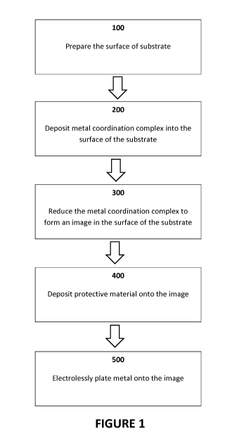
[0016] Figure 1 is an illustrative flow-chart of an exemplary method in
accordance with at
least one embodiment of the present invention;
[0017] Figure 2 illustrates an exemplary bonding in the surface of the
substrate in accordance
with at least one embodiment of the present invention; and
[0018] Figure 3 illustrates exemplary tuned magnetic field states (Figs. 3A
to 3D) in
accordance with at least one embodiment of the present invention.
DETAILED DESCRIPTION OF THE PREFERRED EMBODIMENTS
[0019] The above described drawing figures illustrate the described
invention in at least one
of its preferred, best mode embodiments, which is further defined in detail in
the following
description. Those having ordinary skill in the art may be able to make
alterations and
modifications to what is described herein without departing from its spirit
and scope. While this
invention is susceptible of embodiment in many different forms, there is shown
in the drawings
and will herein be described in detail a preferred embodiment of the invention
with the
understanding that the present disclosure is to be considered as an
exemplification of the
4
CA 02920633 2016-02-05
WO 2015/021202 PCT/US2014/050011
principles of the invention and is not intended to limit the broad aspect of
the invention to the
embodiment illustrated. Therefore, it should be understood that what is
illustrated is set forth
only for the purposes of example and should not be taken as a limitation on
the scope of the
present apparatus and its method of use.
[0020] As shown in Figure 1, in at least one embodiment, a method for
forming a
conductive image using high speed electroless plating comprises the steps of:
preparing the
surface of a substrate; depositing a metal coordination complex into the
surface of the substrate;
reducing the metal coordination complex to form an image in the surface of the
substrate;
depositing a protective material onto the image; electrolessly plating metal
onto the image. As
used herein, a "conductive image" refers to an electrically conductive surface
pattern, for
example and without limitation, that of a printed circuit.
Preparing the Substrate (Step 100)
[0021] As shown in Figure 1, at least a portion of the substrate surface is
prepared to be
electrolessly plated with metal in accordance with Step 100.
[0022] As shown in Figure 2, according to at least one embodiment, a
substrate 10 having a
surface 20 with a thickness 22 is provided and at least a portion of the
substrate surface is
prepared to be electrolessly plated with metal. As used herein, the term "at
least a portion of the
substrate surface" refers to the entire substrate surface or any portion
thereof Preferably, the
substrate is a non-conductive substrate such as, for example, glass, silicone
or polymer. In at
least one embodiment, preparing the substrate surface to be electrolessly
plated with metal
includes at least one of: pretreating the portion the substrate surface, and
activating the portion of
the substrate surface.
[0023] Returning to Figure 1, in at least some embodiments, the step of
preparing the
substrate surface includes pre-treating the portion of the substrate surface,
i.e. removing
unwanted material from the portion of the substrate surface whose presence
during the process of
CA 02920633 2016-02-05
WO 2015/021202 PCT/US2014/050011
the instant invention may result in poor plating. Pretreatment of the
substrate surface may be
accomplished according to known methods in the art.
[0024] In at least some embodiments, the step of preparing the portion of
the substrate
surface includes activating the portion of the substrate surface, i.e.
rendering the substrate surface
more amenable to interaction with and subsequent physical or chemical bonding
to another
material that is disposed onto the surface of the substrate. Activating the
substrate surface may
comprise altering the topography of the substrate surface and/or rendering the
substrate surface
more diffusive to incident electromagnetic radiation.
[0025] In at least one embodiment, activating the substrate surface
comprises altering the
topography of the substrate surface. The topography of the surface can be
altered by any means
known in the art or hereinafter developed, including mechanical, chemical,
plasma, laser or a
combination thereof In at least one embodiment, the topography of the
substrate surface may be
altered via etching, including mechanical, chemical, plasma or laser etching.
[0026] Mechanically altering the substrate surface topology includes, for
example, molding
the substrate with the desired topology. In such embodiments, molten substrate
material may be
deposited into a mold that imparts the desired surface topology to the
produced substrate.
[0027] Chemically altering the substrate surface topology includes, for
example, acid
etching, base etching, oxidative etching and plasma etching. Acid etching
refers to the use of a
strong acid to alter the surface properties of the surface of the substrate,
typically glass, and is
known in the art. Base etching refers to the use of a basic substance to alter
the topology of the
surface of the substrate, typically organic polymers, and is known in the art.
Oxidative etching
refers to the use of a strong oxidant to alter the surface properties of the
surface of the substrate,
and is known in the art.
[0028] Altering the substrate surface topology using plasma includes, for
example, plasma
etching. Plasma etching refers to the process of impacting the surface of a
substrate with a high-
speed stream of a glow discharge of an appropriate gas, and is known in the
art.
6
CA 02920633 2016-02-05
WO 2015/021202 PCT/US2014/050011
[0029] Altering the substrate surface topology using laser includes, for
example, laser
etching. Laser etching refers to the process of directing a laser beam at the
substrate surface so
as to remove material from the substrate surface.
[0030] In at least one embodiment, the topography of the substrate surface
may be altered in
the form of a predetermined pattern or designed topography. As discussed
further herein, the
predetermined pattern may form a trace for the image formed in the substrate
surface. This is
particularly applicable where laser etching is used to prepare the substrate
surface.
[0031] In at least one embodiment, activating the substrate surface
comprises rendering the
substrate surface more diffusive, i.e. permeable to another material that is
disposed into the
surface of the substrate. In such embodiments, the surface of the substrate
may be exposed to a
fluid that softens and/or swells the substrate surface, permitting material
applied to the surface to
physically interact within the surface (i.e. within the surface thickness),
and resulting in the
material being more tightly bonded to the substrate surface ¨ particularly
when dried.
Depositing the Metal Coordination Complex (Step 200)
[0032] As shown in Figure 1, a metal coordination complex is deposited into
the surface of
the portion of the substrate surface in accordance with Step 200.
[0033] According to at least one embodiment, a metal coordination complex
is provided for
deposition into (i.e. within the thickness of) the substrate surface. As used
herein, the term
"metal coordination complex" refers to those metal complexes understood by
those of skill in the
art to have the desired properties described herein. Preferably, the metal
coordination complex is
a para-magnetic or ferro-magnetic metal coordination complex. An exemplary
metal
coordination complex is described, for example, in U.S. Pat. No. 8,784,952 and
U.S. Pat. No.
8,784,953, the entire contents and disclosures of which are herein
incorporated by reference.
7
CA 02920633 2016-02-05
WO 2015/021202 PCT/US2014/050011
[0034]
In at least one embodiment, the metal coordination complex is a ferromagnetic
coordination complex, including iron, nickel or cobalt, preferably iron.
In at least one
embodiment, the metal coordination complex is a paramagnetic coordination
complex, including
tungsten, cesium, aluminum, lithium, magnesium, molybdenum, tantalum,
preferably aluminum
or molybdenum. In at least one embodiment, the metal coordination complex is a
nobel metal
complex, including ruthenium, rhodium, palladium, osmium, iridium, platinum,
silver, copper or
gold, preferably palladium or platinum. In at least one embodiment, the metal
coordination
complex is a combined coordination complex comprising at least one of the
ferromagnetic,
paramagnetic and nobel metal coordinated complexes discussed above.
[0035]
In at least one embodiment, the step of depositing the metal coordination
complex
into the substrate surface comprises the sub-steps of: depositing the metal
coordination complex
onto the substrate surface; applying a magnetic field to the metal
coordination complex so as to
cause the ligands of the metal coordination complex to align and be drawn into
the thickness of
the substrate surface; tuning the magnetic field such that the ligands of the
metal coordination
complex are more aligned and more deeply drawn into the thickness of the
substrate surface; and
removing the magnetic field. In accordance with at least one embodiment, these
sub-steps may
be performed in any order, except that the step of removing the magnetic field
preferably occurs
after the metal coordination complex is applied to the surface of the
substrate under the influence
of the applied magnetic field.
[0036]
In at least one embodiment, the magnetic field is applied by placing the
substrate
surface on or near a source of the magnetic field. Preferably, the magnetic
field is orthogonal to
the substrate surface. The magnetic field may be generated, for example, by
one or more
permanent magnets, electromagnets, or any combination thereof Preferably, the
field strength of
the magnet is at least 1000 Gauss, and more preferably, is at least 2000
Gauss. Preferably, the
magnet is a neodymium magnet. The magnet also has preferred dimensions such
that the portion
of the substrate surface is entirely contained within the dimensions of the
magnet. In some
embodiments, the magnetic field is substantially orthogonal to the portion of
the substrate
surface at all intersecting points and/or has a substantially uniform flux
density. Preferably, the
substrate and the magnet are positioned such that the substrate surface is not
separated from the
8
CA 02920633 2016-02-05
WO 2015/021202 PCT/US2014/050011
magnet by the remainder of the substrate, but is the closest part of the
substrate to the magnet ¨
although alternative configurations are contemplated.
[0037] In at least one embodiment, the magnetic field is a tunable magnetic
field. In other
words, the magnetic field flux density and structure is adjustable or tunable.
In at least one
embodiment, the metal coordination complex is reactive to the applied magnetic
field, and in
particular, to the structure (e.g. magnetic field flux density) of the
magnetic field. Preferably,
application of the tuned magnetic field causes the metal coordination complex
to align according
to the magnetic field structure (e.g. flux density). In at least one
embodiment, the structure of the
magnetic field may be selected based on, at least partially, the actual and/or
desired structural
alignment, shape, polarity and/or depth of the metal coordination complex
within the substrate
surface.
[0038] Figure 3 illustrates exemplary tuned states of the magnetic field.
As shown in
Figures 3A and 3D, for example, the magnetic field may be adjusted between
various tuned
states. Figures 3A and 3B, for example, illustrate elliptical magnetic fields
in flattened (Fig.
3A) and rounded (Fig. 3B) configurations, according to at least one
embodiment. The different
tuned states apply different magnetic forces (both in magnitude and direction)
on the metal
coordination complex, as illustrated by the magnetic field lines in Figure 3.
Accordingly, and
based upon the characteristics of the metal coordination complex, increasing
the amplitude and
power within the electromagnetic field force electrons of the metal
coordination complex to
higher valence levels of bonding. To this effect, the magnetic field may be
tuned to vary (e.g.
make greater) the applied magnetic force, which in turn varies (e.g. makes
stronger) bonding
within the substrate surface.
[0039] In at least one embodiment, depending upon the molecule structure
and polarity of the
metal coordinated complex, each field state may generate different tangent
sites within the
substrate surface to share electrons, causing three different energy level
bonding. Thus, tuning
the magnetic field may comprise combining different electromagnetic field
structures with
different energy levels. For example, as shown in Figures 3C and 3D, a Halbach
Array or
9
CA 02920633 2016-02-05
WO 2015/021202 PCT/US2014/050011
Alternating Polarity array may be utilized to effect the advantages of the
present invention
according to at least one embodiment.
[0040] It should be noted, however, that the exemplary magnetic field
structures described
herein are provided for illustrative purposes, and all conceivable magnetic
field structures.
Moreover, as discussed above, the state of the tuned magnetic field may be
selected according to
the desired metal image to be formed. For example, if it were desired to
electrolessly plate the
entire substrate surface for the purpose of a semi-additive thin layer of
plating, then the magnetic
field may be tuned to reflect a more horizontal, flat, elliptical shape with a
high level of power
(or Gauss). However, if, for example, it were desired to electrolessly plate
high density, fine
features, then the magnetic field may be tuned to set the coordination complex
molecular
structure and alignment such that the plating would build up vertically,
limiting side wall growth.
[0041] Without being held to any particular theory, it is believed that the
metal coordination
complex, under the influence of the magnetic field, will be drawn in toward
the source of the
magnetic field and thereby be more deeply injected into the substrate surface.
Additionally, or in
the alternative, the magnetic field may cause the ligands of the metal
coordination complex to
align in the direction of the magnetic field. Such alignment may further draw
the ligands into the
thickness of the substrate surface. A combination of the two processes may
also occur. The
result in any case is that the metal coordination complex is more tightly
bound within the
substrate surface than which would occur without the influence of the magnetic
field.
[0042] In at least one embodiment, for substrate material commonly use in
the electronics
industry (e.g. glass, etc.), the metal coordination complex penetrates the
thickness of the
substrate surface in excess of a depth of 10%. In at least one embodiment, for
substrate material
commonly use in the electronics industry (e.g. glass, etc.), the metal
coordination complex
penetrates the thickness of the substrate surface in excess of a depth of 15%.
In at least one
embodiment, for substrate material commonly use in the electronics industry
(e.g. glass, etc.), the
metal coordination complex penetrates the thickness of the substrate surface
in excess of a depth
of 20%.
CA 02920633 2016-02-05
WO 2015/021202 PCT/US2014/050011
[0043] In at least one embodiment, after the metal coordination complex is
applied to the
surface of the substrate under the influence of the applied magnetic field,
the source of the
magnetic field is removed.
[0044] In at least one embodiment, the metal coordination complex may be
deposited on the
portion of the substrate surface via painting, spraying, roller applicator, or
any other procedures
known in the art or hereinafter developed. According to at least one
embodiment, the metal
coordination complex may be deposited on the portion of the substrate surface
by inkjet printing.
[0045] In at least one embodiment, the metal coordination complex may be
deposited on the
portion of the substrate in accordance with the image to be formed in the
substrate surface. For
example, a mask may be used to deposit the metal coordination complex in
accordance with the
image to be formed. Accordingly, in some embodiments, the metal coordination
complex is
applied to the predetermined pattern formed in the substrate surface.
[0046] In at least one embodiment, the image comprises an electronic
circuit design.
Preferably, the electronic circuit is selected from the group consisting of an
analog circuit, a
digital circuit, a mixed-signal circuit and an RF circuit. Accordingly, at
least one embodiment
may be practiced to fabricate one or more of: analog circuits, digital
circuits, mixed signal
circuits, and RF circuits.
Forming the Image in the Surface of the Substrate (Step 300)
[0047] As shown in Figure 1, an image is formed in the surface of the
portion of the
substrate surface in accordance with Step 300. The image is a metal image
formed of the metal
coordination complex deposited within the substrate surface reduced to a zero
oxidation state
metal. An exemplary reducing agent and reduction process is described, for
example, in U.S. Pat.
No. 8,784,952 and U.S. Pat. No. 8,784,953, the entire contents and disclosures
of which are
herein incorporated by reference.
11
CA 02920633 2016-02-05
WO 2015/021202 PCT/US2014/050011
[0048] In at least one embodiment, the step of forming an image in the
surface of the
substrate comprises the following sub-steps: exposing the deposited metal
coordination complex
to electromagnetic radiation according to the image to be formed; removing the
unexposed metal
coordination complex so as to leave the metal image; and drying the substrate
surface.
[0049] In at least one embodiment, the step of exposing the deposited metal
coordination
complex to electromagnetic radiation includes exposing the deposited metal
coordination
complex to at least one of: microwave radiation, infrared radiation, visible
light radiation,
ultraviolet radiation, X-ray radiation or gamma radiation. In some
embodiments, the
composition of the metal coordination complex may be such that the metal
coordination complex
is sensitive to a particular range of the electromagnetic spectrum. In
addition, or alternatively,
one or more sensitizers may be added to the metal coordination complex in
association with it
being disposed on the substrate, rendering the coordination complex
photosensitive or, if the
complex is inherently photosensitive, to render it even more so.
[0050] Exposure of the deposited metal coordination complex to
electromagnetic radiation
reduces the metal coordination complex to a zero oxidation state metal by
activating the metal
coordination complex toward a reducing agent. Exposure to radiation renders
the exposed
portion of the metal coordination complex susceptible to reduction. The
reducing agent reduces
the metal coordination complex to elemental metal. The reducing agent may be
any metal-
inclusive salt where the metal has a reduction potential that is greater,
i.e., conventionally has a
more negative reduction potential than the metal of the metal coordination
complex. The result is
that the exposed metal coordination complex is reduced to elemental metal
according to the
metal image.
[0051] In at least one embodiment, the step of removing unexposed (i.e.
unreduced) metal
coordination complex from the substrate surface comprises washing the surface
with a solvent.
The elemental metal image resulting from the exposure (i.e. reduction) step is
preferably
insoluble in most solvents. Thus, washing the surface of the substrate with an
appropriate
solvent, which is determined by the composition of the initial metal
coordination complex, will
remove unexposed complex leaving the metal image. The metal image may be
evenly dispersed
12
CA 02920633 2016-02-05
WO 2015/021202 PCT/US2014/050011
over the surface of the substrate if the surface of the substrate was
generally exposed, or the
metal image may form a discrete pattern if the substrate surface was exposed
according to such.
[0052] In at least one embodiment, once the unexposed metal coordination
complex is
removed, the substrate is dried to complete formation of the metal image. In
at least one
embodiment, the step of drying the surface comprises drying at ambient or
elevated temperature,
preferably, using a vacuum chamber.
[0053] The metal image can then be plated with another metal or coated with
a non-metallic
conductive material.
Depositing the Protective Material onto the Image (Step 400)
[0054] In advance of plating the metal image, a protective layer is
preferably applied to the
metal image (Step 400). This protective layer is preferably a conductive
material. In at least
some embodiments, the protective layer is a metal or conductive polymer that
is applied by at
least one of: flash deposit, vapor deposition, electrostatic bonding, or the
like, all known in the
art.
Electroless Plating Metal onto the Image (Step 500)
[0055] As shown in Figure 1, the protected elemental metal image is
subjected to an
electroless plating process in accordance with Step 500. In this manner a
conductive metal layer
is formed on the regions of the elemental metal image, resulting in a raised
conductive surface.
In at least one embodiment, depositing the conductive metal layer onto the
substrate surface
comprises an accelerated electroless deposition of metal onto the portion of
the substrate surface,
and/or the metal image comprising the reduced metal coordination complex.
[0056] In at least one embodiment, the raised conductive surface comprises
an electronic
circuit. Preferably, the electronic circuit is selected from the group
consisting of an analog
circuit, a digital circuit, a mixed-signal circuit and an RF circuit.
Accordingly, at least one
13
CA 02920633 2016-02-05
WO 2015/021202 PCT/US2014/050011
embodiment may be practiced to fabricate one or more of: analog circuits,
digital circuits, mixed
signal circuits, and RF circuits.
[0057] In at least one embodiment, electroless plating of the metal image
is accomplished by
applying to the substrate surface a solution of a salt of the metal to be
deposited in the presence
of a complexing agent (i.e. a complexed metal salt solution). Application of
the complexed
metal salt solution to the substrate surface may be by brushing, spraying,
submerging or any
other application process known in the art or hereinafter developed. An
aqueous solution of a
reducing agent may be simultaneously or consecutively to the substrate surface
having the
applied complexed metal salt solution. The metal complex is then reduced to
afford elemental
metal which adheres to the metal image already on the surface of the substrate
¨ i.e. an
electrolessly deposited layer of metal on metal results.
[0058] Preferably, the complexing agent keeps the metal ions in solution
and acts to stabilize
the solution, generally. The complexed metal salt solution and the reducing
solution may be
concurrently sprayed onto the patterned substrate either from separate spray
units, the spray
streams being directed so as to intersect at or near the substrate surface, or
from a single spray
unit having separate reservoirs and spray tip orifices, the two streams being
mixed as they
emerge from the spray tip and impinge on the substrate surface.
[0059] In at least one embodiment, electrolessly depositing the conductive
metal layer onto
the portion of the substrate surface comprising the reduced metal coordination
complex
comprises applying to at least the portion of the substrate surface comprising
the metal
coordination complex with a solution comprising a salt of the metal, a
complexing agent and a
reducing agent.
[0060] In at least one embodiment, electrolessly depositing the conductive
metal layer onto
the portion of the substrate surface comprises applying an electroless plating
bath. The
electroless plating solution/bath preferably includes: a
pretreating/cleaning/etching solution for
electroless plating comprising an alkali solution, a reducing agent and a
completing agent; and a
14
CA 02920633 2016-02-05
WO 2015/021202 PCT/US2014/050011
solution/bath of an electroless plating chemistry comprising a pH adjusting
agent, a reducing
agent, a metal ion and a completing agent.
[0061] In at least one embodiment, the pH adjusting agent is preferably
selected from the
group comprising: KOH, NaOH, Ca(OH)2, NH.sub4 OH (with a hydrogen ion
concentration (pH) of 10.5 to 14) or the like.
[0062] In at least one embodiment, the reducing agent is preferably
selected from the group
comprising: an aldehyde, hypophoshites (sodium or potassium), hydrogen borate,
hydrazine,
glyoxylic acid, dimethylamine borane (DMAB), borohydride, cobalt (II)
ethylenediamine
complex, (in a concentration of 2 to 8 percent mo1/1) or the like.
[0063] In at least one embodiment, an accelerator may also be used, and is
preferably
selected from the group comprising: carboxylic acid, glycolic acid, acetic
acid, glycine, oxalic
acid, succinic acid, malic acid, malonic acid, citric acid, phosphinic acid
and nitrilotriacetic acid
(in a concentration of 1 to 20 percent mo1/1) or the like.
[0064] In at least one embodiment, the complexing agent is preferably
selected from the
group comprising: EDTA, HEDTA, Rochelle salt, an organic acid, citric acid,
tartaric acid,
ammonium citrate, TEA, ethylene diamine, trialkyl monoamine, sodium potassium
tartrate,
triisopropanolamine, (in a concentration of 2 to 10 percent mo1/1) or the
like.
[0065] In at least one embodiment, the metal ion is a copper ion of copper
compounds
preferably selected from the group comprising: CuSO4 5H20, CuO,
CuC12,
Cu(NO3)2, (in a concentration of 1 to 5 percent mo1/1).
[0066] In at least one embodiment, the step of subjecting the substrate to
an electroless
plating process comprises agitating the plating solution (i.e. plating bath).
Preferably, agitation
includes nitrogen agitation for approximately 20 to 120 minutes, according to
known methods in
the art.
CA 02920633 2016-02-05
WO 2015/021202 PCT/US2014/050011
[0067] In at least one embodiment, the step of subjecting the substrate to
an electroless
plating process comprises filtering the plating solution (i.e. plating bath).
This is preferably
performed with a less than 1 micron filter, according to known methods in the
art.
[0068] In at least one embodiment, the plating bath contains dissolved
metal salts of the
metal to be plated as well as other ions that render the electrolyte (i.e.
metal salt) conductive.
[0069] When power is applied to the plating bath, including the submerged
substrate surface
portion, the metallic anode is oxidized to produce cations of the metal to be
deposited and the
positively charged cations migrate to the cathode, i.e., the metal image on
the substrate surface,
where they are reduced to the zero valence state metal and are deposited on
the surface.
[0070] In an embodiment of this invention, a solution of cations of the
metal to be deposited
can be prepared and the solution can be sprayed onto the metalized construct.
[0071] The conductive material to be coated on the elemental metal image
may also
comprise a non-metallic conductive substance such as, without limitation,
carbon or a conductive
polymer. Such materials may be deposited on the metal image by techniques such
as, without
limitation, electrostatic powder coating and electrostatic dispersion coating,
which may be
conducted as a wet (from solvent) or dry process. The process may be carried
out by
electrostatically charging the metal image and then contacting the image with
nano- or micro-
sized particles that have been electrostatically charged with the opposite
charge to that applied to
the metal image. In addition, to further ensure that only the metal image is
coated, the non-
conductive substrate may be grounded to eliminate any possibility of an
attractive charge
developing on the substrate or the substrate may be charged with the same
polarity charge as the
substance to be deposited such that the substance is repelled by the
substrate.
Example
[0072] An exemplary embodiment will now be described for illustration.
16
CA 02920633 2016-02-05
WO 2015/021202 PCT/US2014/050011
[0073] For the purpose of showing detailed information and design, the high
speed
electroless process will focus upon copper to be deposited at a higher rate
than the industry
norm, which is 1 -3 per hour, depending upon the electroless copper
chemistries available on
the market, and available. Electroless copper plating has been catalyzed, in
the past, by an active
palladium surface, and continues to deposit auto-catalytically on the newly
reduced copper
deposited. The deposition rate depends upon the half-reaction activity of the
cupric ion reduction
and formaldehyde oxidation on the active palladium and copper surfaces. The
complexing agents
can change the behavior of the half-reactions by stabilizing the cupric ion
through complexation
and by surface adsorption. Let's examine the complexing agents,
ethylenediaminetetraacetic acid
and triethanolamine (for example) on the electrochemical reduction of cupric
ions and the
oxidation of formaldehyde (as the reducing agent). It can also be asserted
that change in pH will
accelerate the deposition rate of the electroless copper. The pH of the
solution influences the
reduction potential through protonation of the coordinated complex or by the
hydroxide acting as
a ligand. The equilibrium potential for the formaldehyde oxidation becomes
more negative with
increasing pH. The use of a complexing agent in the bath is essential because
it prevents the
precipitation of the copper hydroxide under alkaline solutions. The
ethylenediaminetetraacetic
acid based electroless copper solution has a relatively low deposition rate,
with a high bath
stability, because of the strength of the complex with cupric ions (which is
why it is used
primarily in the PCB industry). The past challenge with triethanolamine is
that it can conflict
with the oxidation of formaldehyde and then inhibit the initial copper
deposition on the active
coordination complexes/catalysts. The triethanolamine based electroless copper
solution
achieves a higher deposition rate then the ethylenediaminetetraacetic acid
based solution,
however with the high pH (for acceleration of the deposition rate), it will
remove or impair the
coordinated complex/catalyst from being built upon by the cupric ions.
Therefore, combining the
complexing agent solutions can mitigate the stability issues, or by sealing
the coordination
complex/catalyst with copper, which will allow the accelerated electroless
copper build up, either
will overcome the challenge of the triethanolamine based electroless copper
solution. In the case
of the combination of complexing agents, the deposition rate increases as the
mole ratio of
triethanolamine to ethylenediaminetetraacetic acid increases and the bath
stability is maintained.
Any uneven deposition of copper on the activated surface can be enhanced by
adjusting the
17
CA 02920633 2016-02-05
WO 2015/021202 PCT/US2014/050011
operating temperature and pH of the bath. The net rate of deposition of the
high speed electroless
copper plating occurs at the mixed potential when the cathodic and anodic
currents are equal.
[0074] Experimental Parameters:
[0075] Target pH of solutions should be in the range of 11 to 13 using NaOH
or H2SO4
[0076] Target temperature range should be 45 to 70 C (preferably 55 C)
[0077] Strong nitrogen agitation
[0078] Ratio of components: 1 part copper (0.04M cupric sulfate), 3 parts
reducing agent
(0.12M formaldehyde), and 5 parts complexing agent(s) (0.20M
ethylenediaminetetraacetic acid
and triethanolamine mix) Note: All solutions to be prepared with analytical
grade reagents and
deionized water.
[0079] Use a 5 minute dip of the solution consisting of the Shipley Cuposit
328 material as
follows:328 A 12.5% by volume, 328 L 12.5 % by volume, 328 C 2.5 % by volume,
H20 (De-
Ionized) 72.5% by volume, as the sealant to the aggressive pH in the
triethanolamine solution
prior to the high speed copper electroless tank.
[0080] The reduction performance of cupric ions in alkaline solutions
depends on the
characteristics of the complexing agents utilized. This is because of the
different complexing
abilities as evidenced by their formation constants with cupric ions. Without
the protective
sealant step after the initiation of the coordinated complex/catalyst,
aggressive deposition would
be problematic, however with the institution of this step then the deposition
rate can approach
20 per hour (with increased temperature and pH). By combining the complexing
agents to make
up an aggregate complexing agent with a mixed potential, the oxidation of the
reducing agent is
still independent of the complexing agents but can be accelerated by
increasing pH of the bath.
Ethylenediaminetetraacetic acid and sodium potassium tartrate, both have a
high formation
constant with cupric ions, and therefore a complexing agent based electroless
copper process has
18
CA 02920633 2016-02-05
WO 2015/021202 PCT/US2014/050011
a lower deposition rate and better bath stability with either of these
complexing agents. The
complexing ability of triethanolamine or triisopropanolamine is much lower
than that of
ethylenediaminetetraacetic acid and sodium potassium tartrate, and also could
be detrimental to
the coordination complex/catalyst activation of the substrate surface, unless
the process step of
using a protective layer over the coordination complex/catalyst precedes the
high speed
electroless bath. With the different testing of the potential combinations of
complexing agents
and reducing agents by the above mentioned ratios, it is clear that the
deposition rate increased
with the mole ratio between the aggressive complexing agents and the
complexing agents that
promote stability. The surface coverage and speed of deposition was also
adjusted by the
operating temperature and pH of the bath (as it increased).
[0081] In at least one embodiment, depositing a conductive material onto
the substrate
surface comprises deposition of a non-metallic conductive substance onto the
portion of the
substrate surface, or the image that encompassed or comprising the reduced
metal coordination
complex. In at least one embodiment, the non-metallic conductive material is
deposited onto the
portion of the surface comprising the reduced metal coordination complex by
electrostatic
dispersion. In at least one embodiment, the entire non-conductive substrate
surface is activated
and the metal coordination complex is deposited onto the entire surface. In at
least one
embodiment, the entire non-conductive substrate surface is activated and the
metal coordination
complex is deposited on a part of the activated surface.
[0082] The enablements described in detail above are considered novel over
the prior art of
record and are considered critical to the operation of at least one aspect of
the invention and to
the achievement of the above described objectives. The words used in this
specification to
describe the instant embodiments are to be understood not only in the sense of
their commonly
defined meanings, but to include by special definition in this specification:
structure, material or
acts beyond the scope of the commonly defined meanings. Thus if an element can
be understood
in the context of this specification as including more than one meaning, then
its use must be
understood as being generic to all possible meanings supported by the
specification and by the
word or words describing the element.
19
CA 02920633 2016-02-05
WO 2015/021202 PCT/US2014/050011
[0083] The definitions of the words or drawing elements described herein
are meant to
include not only the combination of elements which are literally set forth,
but all equivalent
structure, material or acts for performing substantially the same function in
substantially the
same way to obtain substantially the same result. In this sense it is
therefore contemplated that an
equivalent substitution of two or more elements may be made for any one of the
elements
described and its various embodiments or that a single element may be
substituted for two or
more elements in a claim.
[0084] As used herein, any term of approximation means that the word or
phrase modified
by the term of approximation need not be exactly that which is written but may
vary from that
written description to some extent. The extent to which the description may
vary will depend on
how great a change can be instituted and have one of ordinary skill in the art
recognize the
modified version as still having the desired properties, characteristics and
capabilities of the
word or phrase unmodified by the term of approximation. In general, but with
the preceding
discussion in mind, a numerical value herein that is modified by a word of
approximation may
vary from the stated value by plus-or-minus 10% unless expressly stated
otherwise.
[0085] Changes from the claimed subject matter as viewed by a person with
ordinary skill in
the art, now known or later devised, are expressly contemplated as being
equivalents within the
scope intended and its various embodiments. Therefore, obvious substitutions
now or later
known to one with ordinary skill in the art are defined to be within the scope
of the defined
elements. This disclosure is thus meant to be understood to include what is
specifically
illustrated and described above, what is conceptually equivalent, what can be
obviously
substituted, and also what incorporates the essential ideas.
[0086] The scope of this description is to be interpreted only in
conjunction with the
appended claims and it is made clear, here, that the named inventor believes
that the claimed
subject matter is what is intended to be patented.