Note: Descriptions are shown in the official language in which they were submitted.
CA 02926625 2016-04-06
WO 2015/057324 PCT/US2014/055179
NON-FARADAIC, CAPACITIVELY COUPLED MEASUREMENT IN A
NANOPORE CELL ARRAY
BACKGROUND OF THE INVENTION
[0001] Advances in micro-miniaturization within the semiconductor
industry in recent
years have enabled biotechnologists to begin packing traditionally bulky
sensing tools into smaller
and smaller form factors, onto so-called biochips. It would be desirable to
develop techniques for
biochips that make them more robust, efficient, and cost-effective.
BRIEF DESCRIPTION OF THE DRAWINGS
[0002] Various embodiments of the invention are disclosed in the
following detailed
description and the accompanying drawings.
[0003] Figure 1 illustrates an embodiment of a cell in a nanopore based
sequencing chip. A
lipid bilayer 102 is formed over the surface of the cell.
[0004] Figure 2 illustrates an embodiment of a cell 200 performing
nucleotide sequencing
with the Nano-SBS technique.
[0005] Figure 3 illustrates an embodiment of a cell performing nucleotide
sequencing with
pre-loaded tags.
[0006] Figure 4 illustrates an embodiment of a process 400 for nucleic
acid sequencing with
"pre-loaded" tags.
[0007] Figure 5A illustrates an embodiment of a small signal circuit
model during faradaic
conduction.
[0008] Figure 5B illustrates the different states of the PNTMC with
faradaic conduction.
[0009] Figure 6 illustrates an embodiment of a cell in a nanopore based
sequencing chip
configured for non-faradaic and capacitively coupled measurements.
[0010] Figure 7 illustrates an embodiment of a small signal circuit model
for non-faradaic
conduction.
1
CA 02926625 2016-04-06
WO 2015/057324 PCT/US2014/055179
[0011] Figure 8A and Figure 8B illustrate an embodiment of the capacitive
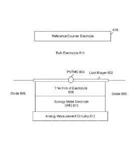
response of the
double layer.
[0012] Figure 9A shows the startup transient when 200 mV with positive
polarity is applied
to the nanopore.
[0013] Figure 9B illustrates the decay rate of the voltage on the double
layer capacitor.
[0014] Figure 10 illustrates that the peak positive current at steady
state varies as a function
of duty cycle and applied voltage.
[0015] Figure 11 illustrates an embodiment of a simulation model that was
matched to the
data of Figure 10.
[0016] Figures 12A and 12B illustrate the simulation result when the
applied signal has a
50% duty cycle.
[0017] Figure 13A illustrates the measurement current when the applied
signal has a 25%
duty cycle.
[0018] Figure 13B illustrates the simulated current when the applied
signal has a 25% duty
cycle.
[0019] Figure 14A illustrates the voltage applied to the nanopore versus
time when the
applied signal has a 50% duty cycle. Figure 14B illustrates the voltage
applied to the nanopore
versus time when the applied signal has a 25% duty cycle.
[0020] Figure 15 illustrates an embodiment of a process for identifying a
molecule.
DETAILED DESCRIPTION
[0021] The invention can be implemented in numerous ways, including as a
process; an
apparatus; a system; a composition of matter; a computer program product
embodied on a computer
readable storage medium; and/or a processor, such as a processor configured to
execute instructions
stored on and/or provided by a memory coupled to the processor. In this
specification, these
implementations, or any other form that the invention may take, may be
referred to as techniques.
In general, the order of the steps of disclosed processes may be altered
within the scope of the
invention. Unless stated otherwise, a component such as a processor or a
memory described as
being configured to perform a task may be implemented as a general component
that is temporarily
2
CA 02926625 2016-04-06
WO 2015/057324 PCT/US2014/055179
configured to perform the task at a given time or a specific component that is
manufactured to
perform the task. As used herein, the term 'processor' refers to one or more
devices, circuits,
and/or processing cores configured to process data, such as computer program
instructions.
[0022] A detailed description of one or more embodiments of the invention
is provided
below along with accompanying figures that illustrate the principles of the
invention. The
invention is described in connection with such embodiments, but the invention
is not limited to any
embodiment. The scope of the invention is limited only by the claims and the
invention
encompasses numerous alternatives, modifications and equivalents. Numerous
specific details are
set forth in the following description in order to provide a thorough
understanding of the invention.
These details are provided for the purpose of example and the invention may be
practiced according
to the claims without some or all of these specific details. For the purpose
of clarity, technical
material that is known in the technical fields related to the invention has
not been described in
detail so that the invention is not unnecessarily obscured.
[0023] Nanopore membrane devices having pore sizes on the order of one
nanometer in
internal diameter have shown promise in rapid nucleotide sequencing. When a
voltage potential is
applied across a nanopore immersed in a conducting fluid, a small ion current
attributed to the
conduction of ions across the nanopore can be observed. The size of the
current is sensitive to the
pore size. When a molecule, such as a DNA or RNA molecule, partially or
completely blocks the
nanopore, the magnitude of the current through the nanopore changes. It has
been shown that the
ionic current blockade can be correlated with the base pair sequence of the
DNA or RNA molecule.
[0024] A nanopore based sequencing chip may be used for DNA sequencing. A
nanopore
based sequencing chip incorporates a large number of autonomously operating
sensor cells
configured as an array. For example, an array of one million cells may include
1000 rows by 1000
columns of cells.
[0025] Figure 1 illustrates an embodiment of a cell in a nanopore based
sequencing chip. A
lipid bilayer 102 is formed over the surface of the cell. The bulk electrolyte
114 containing soluble
protein nanopore transmembrane molecular complexes (PNTMC) and the analyte of
interest is
placed directly onto the surface of the cell. A single PNTMC 104 is inserted
into lipid bilayer 102
by electroporation. The individual lipid bilayers in the array are not
connected to each other either
chemically or electrically. Thus, each cell in the array is an independent
sequencing machine,
producing data unique to the single polymer molecule associated with the
PNTMC. PNTMC 104
operates on the analytes and modulates the ionic current through the otherwise
impermeable
3
CA 02926625 2016-04-06
WO 2015/057324 PCT/US2014/055179
bilayer. The ionic current is read by analog measurement circuit 112 in each
cell, converted to
digital information and transmitted out of the cell. In some embodiments, the
transmission data
rate is on the order of gigabits per second. In some embodiments, a field
programmable gate array
(FPGA) or application-specific integrated circuit (ASIC) receives the
transmitted data, processes
the data, and forwards the data to a computer.
[0026] With continued reference to Figure 1, analog measurement circuitry
112 is
connected to a metal electrode 110 covered by a thin film of electrolyte 108.
The thin film of
electrolyte 108 is isolated from the bulk electrolyte 114 by the ion-
impermeable lipid bilayer 102.
PNTMC 104 crosses lipid bilayer 102 and provides the only path for ionic
current to flow from the
bulk liquid to metal electrode 110. Metal electrode 110 is also referred to as
the working electrode
(WE). The cell also includes a counter/reference electrode (CE/RE) 116, which
is an
electrochemical potential sensor.
[0027] In some embodiments, a nanopore array enables parallel sequencing
using the single
molecule nanopore-based sequencing by synthesis (Nano-SBS) technique. Figure 2
illustrates an
embodiment of a cell 200 performing nucleotide sequencing with the Nano-SBS
technique. In the
Nano-SBS technique, a template 202 to be sequenced and a primer are introduced
to cell 200. To
this template-primer complex, four differently tagged nucleotides 208 are
added to the bulk
aqueous phase. As the correctly tagged nucleotide is complexed with the
polymerase 204, the tail
of the tag is positioned in the vestibule of nanopore 206. The tails of the
tags can be modified to
have strong affinity with the amino acid residues in the vestibule of nanopore
206. After
polymerase catalyzed incorporation of the correct nucleotide, the tag-attached
polyphosphate is
released and passes through nanopore 206 to generate a unique ionic current
blockade signal 210,
thereby identifying the added base electronically due to the tags' distinct
chemical structures.
[0028] Figure 3 illustrates an embodiment of a cell performing nucleotide
sequencing with
pre-loaded tags. A nanopore 301 is formed in a membrane 302. An enzyme 303
(e.g., a
polymerase, such as a DNA polymerase) is associated with the nanopore. In some
cases,
polymerase 303 is covalently attached to nanopore 301. Polymerase 303 is
associated with a single
stranded nucleic acid molecule 304 to be sequenced. In some embodiments,
single stranded nucleic
acid molecule 304 is circular. In some cases, nucleic acid molecule 304 is
linear. In some
embodiments, a nucleic acid primer 305 is hybridized to a portion of nucleic
acid molecule 304.
Polymerase 303 catalyzes the incorporation of nucleotides 306 onto primer 305
using single
stranded nucleic acid molecule 304 as a template. Nucleotides 306 comprise tag
species ("tags")
307.
4
CA 02926625 2016-04-06
WO 2015/057324 PCT/US2014/055179
[0029] Figure 4 illustrates an embodiment of a process 400 for nucleic
acid sequencing with
"pre-loaded" tags. Stage A illustrates the components as described in Figure
3. Stage C shows the
tag loaded into the nanopore. A "loaded" tag may be one that is positioned in
and/or remains in or
near the nanopore for an appreciable amount of time, e.g., 0.1 millisecond
(ms) to 1000 ms. In
some cases, a tag that is "pre-loaded" is loaded in the nanopore prior to
being released from the
nucleotide. In some instances, a tag is pre-loaded if the probability of the
tag passing through
(and/or being detected by) the nanopore after being released upon a nucleotide
incorporation event
is suitably high, e.g., 90% to 99%.
[0030] At stage A, a tagged nucleotide (one of four different types: A,
T, G, or C) is not
associated with the polymerase. At stage B, a tagged nucleotide is associated
with the polymerase.
A voltage (e.g., a DC or AC voltage) may be applied to the nanopore or the
membrane in which the
nanopore resides to draw the polymerase to the nanopore. At stage C, the
polymerase is docked to
the nanopore. The tag is pulled into the nanopore during docking by an
electrical force, such as a
force generated in the presence of an electric field generated by a voltage
applied across the
membrane and/or the nanopore.
[0031] Some of the associated tagged nucleotides are base paired with the
single stranded
nucleic acid molecule (e.g., A with T and G with C). However, some of the
associated tagged
nucleotides are not base paired with the single stranded nucleic acid
molecule. These non-paired
nucleotides typically are rejected by the polymerase within a time scale that
is shorter than the time
scale for which correctly paired nucleotides remain associated with the
polymerase. Since the non-
paired nucleotides are only transiently associated with the polymerase,
process 400 as shown in
Figure 4 typically does not proceed beyond stage D. For example, a non-paired
nucleotide is
rejected by the polymerase at stage B or shortly after the process enters
stage C.
[0032] Before the polymerase is docked to the nanopore, the current
passing through the
nanopore is ¨30 picoamps (pA). At stage C, the current flowing through the
nanopore is about 6
pA, 8 pA, 10 pA, or 12 pA, each amperage corresponding to one of the four
types of tagged
nucleotides. The polymerase undergoes an isomerization and a
transphosphorylation reaction to
incorporate the nucleotide into the growing nucleic acid molecule and release
the tag molecule. At
stage D, the released tag passes through the nanopore. The tag is detected by
the nanopore. In
particular, as the tag passes through the nanopore, a unique ionic current
blockade signal (e.g., see
signal 210 in Figure 2) is generated due to the tag's distinct chemical
structures, thereby identifying
the added base electronically. Repeating the cycle (i.e., stage A through E or
stage A through F)
allows for the sequencing of the nucleic acid molecule.
CA 02926625 2016-04-06
WO 2015/057324
PCT/US2014/055179
[0033] In some cases, tagged nucleotides that are not incorporated into
the growing nucleic
acid molecule will also pass through the nanopore, as seen in stage F of
Figure 4. The un-
incorporated nucleotide can be detected by the nanopore in some instances, but
the method
provides a means for distinguishing between an incorporated nucleotide and an
un-incorporated
nucleotide based at least in part on the time for which the nucleotide is
detected in the nanopore.
Tags bound to un-incorporated nucleotides pass through the nanopore quickly
and are detected for
a short period of time (e.g., less than 10 ms), while tags bound to
incorporated nucleotides are
loaded into the nanopore and detected for a long period of time (e.g., at
least 10 ms).
[0034] Two types of ionic flow can be driven through the PNTMC ¨ faradaic
conduction
and non-faradaic conduction. In faradaic conduction, a chemical reaction
occurs at the surface of
the metal electrode. The faradaic current is the current generated by the
reduction or oxidation of
some chemical substances at an electrode. In non-faradaic conduction, no
chemical reaction
happens at the surface of the metal. The changing potential on the double
layer capacitance
between the metal electrode and the thin film of electrolyte drives the ion
flow.
[0035] Ionic flow by faradaic conduction has a number of drawbacks. The
operational
lifespan of an electrode is limited because the metal in the electrode is
consumed and depleted as
the ionic current flows through the PNTMC, as will be described in greater
detail below.
[0036] Figure 5A illustrates an embodiment of a small signal circuit
model during faradaic
conduction. The PNTMC and WE are represented as simple resistors in the small
signal circuit
model. Figure 5B illustrates the different states of the PNTMC with faradaic
conduction. The
ionic current flow, i(t), has five states: the highest current state with an
open nanopore channel (not
shown) and four lower current states corresponding to each of four different
types of nucleotides
bound to the active site of the PNTMC. Positive current flow i(t) describes
electrons entering the
VcE, RE node and leaving the VwE node. Anions (e.g., C1-) leave the CE, flow
through the bulk
electrolyte, cross the lipid bilayer via the PNTMC, and continue through the
thin film of electrolyte
and combine with the metal of the WE.
[0037] For example, for an electrode with silver metal (Ag), the chemical
reaction is:
Ag (solid) + Cl(¨aqueous) ¨) A9C1(5oud) + electron(flows in analog circuit)
Equation 1
[0038] As shown in Equation 1 above, an atom of metallic silver is
converted to an
insoluble salt, silver-chloride (AgC1), for each chloride anion (CY) that
passes through the PNTMC.
In some cases, the silver is depleted within minutes of operation.
6
CA 02926625 2016-04-06
WO 2015/057324 PCT/US2014/055179
[0039] To avoid depletion of the metal electrode, the direction of the
ionic current flow may
be reversed by applying a negative voltage for a similar duration, causing the
silver-chloride
(AgC1) to be converted back to silver metal. However, recharging or refreshing
in this manner
causes the silver to be re-deposited as hair-like features on the surface of
the metal electrode, which
may impact overall performance, especially in chips with smaller cell geometry
and thus smaller
electrodes.
[0040] Another way is to delay the depletion of the metal electrode by
applying a voltage to
draw the polymerase to the nanopore and pull the tag through or to the
proximity of the nanopore
for detection, and then turn off the voltage for a period of time, which will
cause the tag to be
released from the nanopore. Since there is no current while the voltage is
turned off, fewer silver
atoms are converted and the lifespan of the metal electrode is prolonged.
However, the detection
time is reduced accordingly.
[0041] In addition to depletion of the metal electrode, faradaic
conduction also causes an
imbalance in the concentration of the bulk electrolyte within the cells over
time. For example,
there is a net gain of KC1 molecules at one electrode but a net loss of KC1
molecules at the opposite
electrode. This salt concentration buildup at one electrode and salt depletion
on the opposite
electrode creates undesirable osmotic pressure within the cell.
[0042] An alternative type of ionic flow through the PNTMC is via non-
faradaic
conduction. In non-faradaic conduction, no chemical reaction (reduction or
oxidation of chemical
substances) occurs at the surface of the metal. The changing potential across
the double layer
capacitance between the metal electrode and the thin film of electrolyte
drives the ion flow.
[0043] For non-faradaic conduction, the metal electrode may be made of
metals that are
resistant to corrosion and oxidation. For example, noble metals such as
platinum or gold oxidize
with difficulty, and even when they do oxidize, the process is easily
reversible. When small
potentials (e.g., less than +/- 1 V relative to VcE) are applied to
platinum/gold in an electrolyte,
aside from an initial capacitive transient, no ionic current flows. This
allows the measurement of
electron tunneling from the metal into redox (reduction-oxidation) active
species mixed into the
electrolyte. Without redox active species (such as Ferricyanide or
Ferrocyanide) in the electrolyte,
no steady state ionic (or electron or hole) current flows across the metal-
liquid interface. Despite
the lack of chemical (i.e., bonding) interaction between the platinum/gold and
the electrolyte, there
is transient physical displacement of ions in the electrolyte from the growth
and shrinkage of the
ion depletion region at the metal-liquid interface, in response to the applied
potential. This ion
7
CA 02926625 2016-04-06
WO 2015/057324 PCT/US2014/055179
depletion region is referred to as a "double layer" in electrochemistry
parlance. Using an electrical
engineering model, a parallel plate capacitor forms where the metal is one
plate, the depletion
region is the dielectric, and the diffuse distribution of ions in the liquid
is the other plate.
[0044] Figure 6 illustrates an embodiment of a cell in a nanopore based
sequencing chip
configured for non-faradaic and capacitively coupled measurements. A lipid
bilayer 602 is formed
over the surface of the cell. The electrolyte containing soluble protein
nanopore transmembrane
molecular complexes (PNTMC) and analyte of interest 614 is placed directly
onto the surface of
the cell. A single PNTMC 604 is inserted into lipid bilayer 602 by
electroporation. The individual
lipid bilayers in the array are not connected to each other either chemically
or electrically. Thus,
each cell in the array is an independent sequencing machine producing data
unique to the single
polymer molecule associated with the PNTMC. The cell includes an analog
measurement circuit
612 for making non-faradaic and capacitively coupled measurements. The
measurements are
converted to digital information and transmitted out of the cell. In some
embodiments, the
transmission data rate is on the order of gigabits per second. In some
embodiments, a field
programmable gate array (FPGA) or an application-specific integrated circuit
(ASIC) receives the
transmitted data, processes the data, and forwards the data to a computer.
[0045] With continued reference to Figure 6, analog measurement circuitry
612 is
connected to a metal electrode 610 covered by a thin film of electrolyte 608.
The thin film of
electrolyte 608 is isolated from the bulk electrolyte 614 by the ion-
impermeable lipid bilayer 602.
PNTMC 604 crosses lipid bilayer 602 and provides the only path for ionic flow
from the bulk
liquid to metal electrode 610. Metal electrode 610 is also referred to as the
working electrode
(WE). For non-faradaic conduction, metal electrode 610 may be made of metals
that are resistant
to corrosion and oxidation, e.g., platinum, gold, and graphite. Metal
electrode 610 may be a
spongy electrode, as will be described in greater detail below. The cell also
includes a
counter/reference electrode (CE/RE) 616, which is an electrochemical potential
sensor.
[0046] Figure 7 illustrates an embodiment of a small signal circuit model
for non-faradaic
conduction. The PNTMC is represented as a simple resistor 702 in the small
signal circuit model.
The double layer capacitance is represented as a capacitor 704 in the small
signal circuit model. In
some embodiments, V1 in Figure 7 is set to be an incremental voltage from
ground, e.g., 500 mV,
while V2 is set to be V1 plus an applied signal, e.g., an applied AC signal
from 10Hz to lkHz.
[0047] In some embodiments, the applied signal is an AC signal. At one
polarity, the
applied AC signal draws the polymerase to the nanopore and draws the tag
through or to the
8
CA 02926625 2016-04-06
WO 2015/057324 PCT/US2014/055179
proximity of the nanopore for detection. When the polarity of the applied AC
signal is reversed,
the tag is released from the nanopore, and the electrode is
recharged/refreshed such that no
electrochemical changes are made to the metal electrodes. As the AC signal
repeatedly changes
polarity, a portion of a tag associated with a tagged nucleotide is directed
into a nanopore and
directed out of the nanopore for a plurality of times. This repetitive loading
and expulsion of a
single tag allows the tag to be read multiple times. Multiple reads may enable
correction for errors,
such as errors associated with tags threading into and/or out of a nanopore.
[0048] In some embodiments, the frequency of the AC signal is chosen at
least in part based
on the time period during which a tagged nucleotide is associated with a
polymerase. The
frequency of the AC signal should allow a tagged nucleotide associated with
the polymerase to be
drawn and loaded into the nanopore for a sufficient length of time at least
once such that the tag can
be detected; otherwise, some of the tags that are associated with the
polymerase cannot be detected
by the system. In other words, the sampling should be at a rate faster than
the rate at which the
sequence of events is occurring, such that no events are missed.
[0049] With continued reference to Figure 6, before the lipid bilayer 602
has been formed,
the bulk electrolyte 614 is in direct contact with the working electrode 610,
thus creating a short
circuit between the electrolyte and the working electrode. Figure 8A and
Figure 8B illustrate an
embodiment of the capacitive response of the double layer. The figures
illustrate the properties of
the double layer with a short circuit between the electrolyte and the working
electrode. In this
example, the electrolyte contains 0.5 M Potassium Acetate and 10mM KC1. The
counter electrode
616 includes AgCl. The working electrode 610 is a platinum electrode with
electroplated platinum.
Water viscosity prevents the easy flow of ions in response to the applied
field; this is manifested as
a series resistance in the double layer capacitive response. This resistance
limits the peak current as
shown in Figure 8A. The series nature of the RC electrochemical connection can
be seen in the
decay of the response, which is characterized by the RC time constant. In
Figure 8B, the current is
shown to fall to exp (-25) = 13.8 pA, below the detection limit of the system.
This demonstrates a
lack of both shunt resistance (from an electrical point of view) and faradaic
current (from an
electrochemical point of view).
[0050] The working electrode 610 is configured to maximize its surface
area for a given
volume. As the surface area increases, the capacitance of the double layer
increases, and a greater
amount of ions can be displaced with the same applied potential before the
capacitor becomes
charged. Referring to Figure 7, the impedance of CDouble Layer ¨ (j*2*pi* f*C)
, where f = frequency
9
CA 02926625 2016-04-06
WO 2015/057324 PCT/US2014/055179
and C = CDouble Layer By making f, C, or both f and C larger, the capacitor's
impedance becomes
very small relative to RpNTmc, and the current to be measured becomes larger.
As the impedance of
the small signal model is dominated by RpNTmc, the measured current can better
differentiate the
five states: the highest current state with an open nanopore channel and four
lower current states
corresponding to each of four different types of nucleotides bound into the
active site of the
PNTMC.
[0051] For example, the surface area of the working electrode may be
increased by making
the electrode "spongy." In some embodiments, the capacitance of the double
layer to the bulk
liquid can be enhanced by electroplating platinum metal onto a 5 micron
diameter smooth platinum
electrode in the presence of a detergent. The detergent creates nanoscale
interstitial spaces in the
platinum metal, making it "spongy." The platinum sponge soaks up electrolyte
and creates a large
effective surface area (e.g., 33 pF per square micron of electrode top-down
area). Maximizing the
double layer surface area creates a "DC block" capacitor, whereby the voltage
on the double layer
reaches steady state and barely changes during operation. The series PNTMC
resistance (RPNTMC in
Figure 7) and the double layer capacitance (CDouble Layer in Figure 7) form a
low frequency zero,
which acts as a high pass filter. In one example, RPNTMC ¨ 10 gigaohm, CDouble
Layer ¨800pF,
resulting in a time constant of ¨10 gigaohm * ¨800pF = ¨8 second time
constant. Chopping the
measurement at 100 Hz then rejects DC drift and attenuates low frequency
information content in
the measured tags by a factor of 1000.
[0052] Without any tags present, the PNTMC behaves similar to an alpha
hemolysin
protein nanopore. The hemolysin nanopore has a rectifying characteristic which
changes its bias
depending on the duty cycle of the square wave drive. Unlike the faradaic
conduction case, the
absolute voltage applied to the electrode is not the same as the voltage
applied to the nanopore: the
voltage on the double layer biases the potential applied to the nanopore, and
this bias changes with
the duty cycle.
[0053] Figures 9A and 9B illustrate the nanopore current with non-
faradaic AC modulation.
In this example, the applied signal is a 200 mV peak to peak square wave with
a 50% duty cycle at
Hz. The electrolyte contains 0.5 M Potassium Acetate and 10mM KC1. The counter
electrode
616 includes AgCl. The working electrode 610 is a platinum electrode with
electroplated platinum.
[0054] Figure 9A shows the startup transient when 200 mV with positive
polarity is applied
to the nanopore, indicating that the open channel current with 200 mV directly
applied is
approximately 70 pA. Figure 9A shows that the steady state is reached after
¨20 seconds. In
CA 02926625 2016-04-06
WO 2015/057324 PCT/US2014/055179
Figure 9B, the decay rate of the voltage on the double layer capacitor can be
observed. The decay
rate is determined by the size of the double layer capacitance and the
nanopore load resistance.
[0055] Figure 10 illustrates that the peak positive current at steady
state varies as a function
of duty cycle and applied voltage. Plot 1010 shows the steady state peak
current in amperes (A)
plotted against different duty cycles when the applied voltage is a 200 mV
peak to peak square
wave. Plot 1020 shows the steady state peak current (in A) plotted against
different duty cycles
when the applied voltage is a 100 mV peak to peak square wave. In this
example, the electrolyte
contains 0.5 M Potassium Acetate and 10mM KC1. The counter electrode 616
includes AgCl. The
working electrode 610 is a platinum electrode with electroplated platinum.
Since the hemolysin
nanopore has a rectifying characteristic (or is non-ohmic), a larger magnitude
negative polarity
voltage is required to pass the same magnitude of current than when a positive
polarity voltage is
applied. The peak positive current drops as the duty cycle is increased. The
lower the duty cycle,
the higher the positive voltage applied to the nanopore through the double
layer capacitance.
[0056] Figure 11 illustrates an embodiment of a simulation model that was
matched to the
data of Figure 10. The simulation is constructed to estimate the actual
voltage on the nanopore,
which is not the same as the voltage applied to the working electrode because
of the double layer
capacitor connected in series with the nanopore. This voltage cannot be
directly measured in the
non-faradaic cases. The non-linearlity in potassium acetate was assumed to be
directly proportional
to the 1 M potassium chloride non-linearity. Figures 12A and 12B illustrate
the simulation result
when the applied signal has a 50% duty cycle. In Figure 12B, the slope of the
decay is steeper for
the positive current than the negative current because of the rectifying
characteristics of the
hemolysin nanopore, which is modeled with the polynomial equations B1 and B2
in Figure 11.
[0057] Figure 13A illustrates the measurement current when the applied
signal has a 25%
duty cycle. Figure 13B illustrates the simulated current when the applied
signal has a 25% duty
cycle. These figures illustrate that with a lower duty cycle of 25%, the
magnitude of the positive
current (43pA) through the nanopore is much larger than the magnitude of the
negative current (-13
pA) through the nanopore. In order to achieve no shunt resistance (no faradaic
current) at steady
state, the sum of the positive and negative charge through the double layer
over one period of
oscillation should be zero. As i = dQ/dt, where i = current and Q = charge, in
a graph of current
versus time, charge is the area under the curve. For example, if the area
under the curve of the
current versus time plot of positive polarity (area 1302 of Figure 13B) is
roughly the same as the
area under the curve of the current versus time plot of negative polarity
(area 1304 of Figure 13B),
11
CA 02926625 2016-04-06
WO 2015/057324 PCT/US2014/055179
then the sum of the positive and negative charge through the double layer over
one period of
oscillation is close to zero.
[0058] Figure 14A illustrates the voltage applied to the nanopore versus
time when the
applied signal has a 50% duty cycle. Figure 14B illustrates the voltage
applied to the nanopore
versus time when the applied signal has a 25% duty cycle. With a lower duty
cycle in Figure 14B,
the voltage applied to the nanopore is higher, which draws the polymerase and
the tag towards the
nanopore with greater efficacy. With a longer duty cycle in Figure 14A, more
time is spent in
reading and detecting the tag while a nucleotide specific tail is in place.
[0059] Figure 15 illustrates an embodiment of a process for identifying a
molecule. At
1502, a molecule is drawn to a nanopore by applying a first voltage signal to
a pair of electrodes
(e.g., the working electrode and the counter/reference electrode) during a
first period, wherein the
first voltage signal causes a first ionic current through the nanopore that is
indicative of a property
of a portion of the molecule (e.g., a tagged nucleotide) proximate to the
nanopore. For example,
the four types of tagged nucleotides have different properties and when a
particular type of tagged
nucleotide is drawn into the nanopore, an ionic current indicative of the
property flows through the
nanopore.
[0060] At 1504, the molecule is released from the nanopore by applying a
second voltage
signal to the pair of electrodes during a second period, wherein the second
voltage signal causes a
second ionic current through the nanopore.
[0061] At 1506, the first period and the second period are determined
based at least in part
on a net ionic current through the nanopore comprising the first ionic current
and the second ionic
current. For example, the first period and the second period can be determined
such that the net
ionic current is reduced. In some embodiments, the net ionic current is
reduced by setting the
second voltage signal to off When the second voltage signal is turned off, the
second ionic current
becomes zero and the depletion of the metal electrode is delayed as explained
above. In some
embodiments, the net ionic current is reduced by setting the second voltage
signal to a signal with a
polarity opposite from the first voltage signal. For example, alternating
between the first voltage
signal and the second voltage signal makes an AC signal. The second ionic
current offsets the first
ionic current, thus reducing the net ionic current through the nanopore. As
shown in Figure 10, the
current varies as a function of duty cycle and applied voltage. Therefore, the
duty cycle (i.e., the
first period and the second period) can be adjusted such that the area under
the curve of the first
ionic current is substantially the same as the area under the curve of the
second ionic current such
12
CA 02926625 2016-04-06
WO 2015/057324 PCT/US2014/055179
that the sum of the positive and negative charge through the double layer over
one period of
oscillation (i.e., the first period and the second period) is close to zero.
[0062] Although the foregoing embodiments have been described in some
detail for
purposes of clarity of understanding, the invention is not limited to the
details provided. There are
many alternative ways of implementing the invention. The disclosed embodiments
are illustrative
and not restrictive.
13