Note: Descriptions are shown in the official language in which they were submitted.
MGR FREQUENCY ARRAY ULTRASOUND SYSTEM
BACKGROUND OF THE INVENTION
Ultrasound. echography systems using an arrayed transducer have been used in
hmnan
clinical applications where the desired image resolution is in the order
ofmillimeters. Operating
frequencies in these clinical systems are typically below 10 MHz. With these
low operating
frequencies, however, such systems are not appropriate forimaging where higher
resolutions are
needed, for example in imaging small animals such as nice or small tissue
structures in humans.
Moreover, small animal imaging applications present several challenging
requirements
which are not met by currently available imaging syatems. The heart rate of
an adult mouse may
be as high as 500 beats per minute, sold& frame rate capabilitymaybe desired.
The width ofthe
region being imaged, the field of view, should also be sufficient to include
the entire organbeing
studied.
Ultrasound systems for imaging at frequencies above 151VIElz have been
developedusing
a single element transducer., However, arrayedtransducers offer better image
quality, can achieve
higher acquisition frame rates and offer other advantages over single element
transducer systems.
The embodiments according to the present invention overcome many of the
challenges in the
current art, including those described above.
= 25 SUIVIMARY OF TEE INVENTION.
Provided herein is a system and method for acquiring an ultiasonnd signal
comprised of a.
signal processing wait adapted for acquiring a received ultrasound signal from
a ultrasound
transducer having a plurality of elements. The system can be adapted to
receive ultrasound
= signals having a frequency of at least 15 megahertz (MHz) with a fixed
transducer having a field
of view of at least 5.0 millimeters (mm) at a frame rate of at least 20 frames
per second (fps).
The signl processing unit can firrtherproduce anultrasound image fromthe
acquiredultrasound
signal. The transducer can be, but is not limited to, a linear array
transducer, a phased array
-; transducer, a two-dimensional (2-D) array transducer, or a curved
array transducer. The system
- 1 -
CA 2935422 2017-11-23
CA 02935422 2016-07-06
can include such a transducer or be adapted to operate with such a transducer.
Also provided herein is a system and method for acquiring an ultrasound signal
comprising a processing unit for acquiring received ultrasound signals from an
ultrasound
transducer operating at a transmit and receive frequency of at least 15 MHz,
wherein the
processing unit comprises a signal sampler that uses quadrature sampling to
acquire the
ultrasound signal.
Additional advantages of the invention will be set forth in part in the
description which
follows, and in part will be obvious from the description, or may be learned
by practice of the
invention. The advantages of the invention will be realized and attained by
means of the
elements and combinations particularly pointed out in the appended claims. It
is to be understood
that both the foregoing general description and the following detailed
description are exemplary
and explanatory only and are not restrictive of the invention, as claimed.
- 2 -
CA 02935422 2016-07-06
BRIEF DESCRIPTION OF THE DRAWINGS
The accompanying drawings, which are incorporated in and constitute a part of
this
specification, illustrate several embodiments according to the invention and
together with the
description, serve to explain the principles of the invention:
FIG. 1 is a representation in block diagram form of a computing operating
environment;
FIGS. 2A-2C, are exemplary top, bottom and cross-sectional views of an
exemplary
schematic PZT stack of the present invention, the top view showing, at the top
and bottom of the
PZT stack, portions of the ground electric layer extending outwardly from the
overlying lens; the
bottom view showing, at the longitudinally extending edges, exposed portions
of the dielectric
layer between individual signal electrode elements (as one will appreciate,
not show in the center
portion of the PZT stack are the lines showing the individualized signal
electrode elements ¨ one
signal electrode per element of the PZT stack);
FIG. 3A is a top plan view of an interposer for use with the PZT stack of
FIGS. 2A-2C,
showing electrical traces extending outwardly from adjacent the central
opening of the transducer
and ground electrical traces located at the top and bottom portions of the
interposer, showing a
dielectric layer disposed thereon a portion of the surface of the interposer,
the dielectric layer
defming an array of staggered wells positioned along an axis parallel to the
longitudinal axis of
the interposer, each well communicating with an electrical trace of the
interposer, and further
showing a solder paste ball bump mounted therein each well in the dielectric
layer such that,
when a PZT stack is mounted thereon the dielectric layer and heat is applied,
the solder melts to
form the desired electrical continuity between the individual element signal
electrodes and the
individual trances on the interposer ¨ the well helping to retain the solder
within the confines of
the well;
FIG. 3B is a partial enlarged view of the staggered wells of the dielectric
layer and the
electrical traces of the underlying interposer of FIG. 3A, the well sized to
accept the solder paste
ball bumps;
FIG. 4A is a top plan view of the PZT stack of FIG. 2A mounted thereon the
dielectric
layer and the interposer of FIG. 3A;
FIG. 4B is a top plan view of the PZT stack of FIG. 2A mounted thereon the
dielectric
layer and interposer of FIG. 3A, showing the PZT stack as a transparent layer
to illustrate the
mounting relationship between the PZT stack and the underlying interposer, the
solder paste ball
bumps mounted therebetween forming an electrical connection between the
respective element
signal electrodes and the electrical traces on the interposer;
- 3 -
CA 02935422 2016-07-06
FIG. 5A is a schematic top plan view of an exemplary circuit board for
mounting the
transducer of the present invention thereto, the circuit board having a
plurality of board electrical
traces formed thereon, each board electrical trace having a proximal end
adapted to couple to an
electrical trace of the transducer and a distal end adapted to couple to a
connector, such as, for
example, a cable for communication of signals therethrough;
FIG. 5B is a top plan view of an exemplary circuit board for mounting of an
exemplary
256-element array having a 75 micron pitch;
FIG. 5C is a top plan view of the vias of the circuit board of FIG. 5B that
are in
communication with an underlying ground layer of the circuit board;
FIG. 6 is a top plan view of a portion of the exemplified circuit board
showing, in Region
A, the ground electrode layer of the transducer wire bonded to an electrical
trace on the
interposer, which is, in turn, wire bonded to ground pads of the circuit
board, and further
showing, in Region B, the individual electrical traces of the transducer wire
bonded to individual
board electrical traces of the circuit board;
FIG. 7A is a partial enlarged cross-sectional view of Region A of FIG. 6,
showing the
dielectric layer positioned about the solder paste ball bumps and between the
PZT stack and the
interposer;
FIG. 7B is a partial enlarged cross-sectional view of Region B of FIG. 6,
showing the
dielectric layer between the PZT stack and the interposer;
FIGS. 8A and 8B are partial cross-sectional views of an exemplified transducer
mounted
to a portion of the circuit board;
FIG. 9 is an enlarged partial view Region B of an exemplified transducer
mounted to a
portion of the circuit board;
FIG. 10 is a partial enlarged cross-sectional view of a transducer that does
not include an
interposer, showing a solder paste ball bump mounted thereon the underlying
circuit board, each
ball bump being mounted onto one board electrical trace of the circuit board,
and showing the
PZT stack being mounted thereon so that the respective element signal
electrodes of the PZT
stack are in electrical continuity, via the respective ball bumps, to their
respective board electrical
trace of the circuit board;
FIG. 11A is a partial enlarged cross-sectional view of FIG. 10, showing the
ground
electrode layer of the transducer without an interposer wire bonded to ground
pads of the circuit
board;
- 4 -
CA 02935422 2016-07-06
FIG. 11B is a partial enlarged cross-sectional view of FIG. 10, showing the
ball bump
disposed therebetween and in electrical communication with the electrical
trace of the circuit
board and the element signal electrode of the PZT stack;
FIG. 12A is a schematic showing the flex circuit board and a pair of Sanitec
BTH-090
connectors mounted to a rigid portion of the circuit board;
FIG. 12B is an exemplary pin-out table for the connector shown in FIGS. 5B and
12A;
FIG. 13 is a schematic showing a side view of the individual coaxial cables
that are to be
operatively coupled to the pair of Samtec BTH-090 connectors on the flex
circuit board via a pair
of BSH-090 connectors;
FIG. 14 is a schematic showing an exemplary plan view of half of the coaxial
leads
therein the cable connected to one of the BSH-090 connectors;
FIG. 15A is an illustration of an exemplary plan view of the distal end of a
medical cable
assembly connected to the folded flex circuit board, the cable's proximal end
(not shown) may
include a multi-pin ZIF connector that interfaces with the ultrasound system
and may be used to
practice one or more aspects of the present invention;
FIG. 15B illustrates an exemplary termination pin-out for the individual coax
cables of a
medical cable assembly to a multi-pin ZIP connector having an exemplary Lit'
connector such as
an ITT Cannon DLM6 connector;
FIG. 16 is a block diagram illustrating an exemplary high frequency ultrasonic
imaging
system;
FIG. 17 is a block diagram further illustrating the exemplary high frequency
ultrasonic
imaging system shown in FIG. 16;
FIG. 18a is a schematic diagram illustrating exemplary receive beamformers,
transmit
beamformers, front end electronics, and associated components;
FIG. 18b is an exemplary embodiment providing additional detail of the front
end
electronics shown in FIG. 18a;
FIG. 18c is an exemplary embodiment of a receive controller (RX controller) in
an
embodiment according to the present invention
FIG. 18d is an illustration of an exemplary transmit controller (TX
controller) in an
embodiment according to the present invention
FIG. 19 is a system signal processing block diagram illustrating an exemplary
beamformer control board;
FIG. 20 is a schematic diagram of a TXTRX Switch and Pulser and related
circuitry;
- 5 -
CA 02935422 2016-07-06
FIG. 21 is a schematic diagram of an alternative embodiment of a TX/RX Switch
and
Pulser and related circuitry;
FIG. 22 is a block diagram for an exemplary transmit beamformer control;
FIGS. 22A-22C illustrate how exemplary waveshape data can be used to change
the fine
delay, pulse width and dead time for "A" and "B" signals;
FIG. 24 illustrates a systems electronics overview of an exemplary high
frequency
ultrasonic imaging system;
FIG. 25 shows an exemplary single channel delay scheme for quadrature
sampling;
FIG. 25B is an alternative way of implementing interpolation filters, phase
rotation and
dynamic apodization according to an embodiment of the invention;
FIG. 26 illustrates an exemplary control RAM for storing receive control
signals;
FIG. 26A shows exemplary beamformer delay control signals for center and outer
elements of an arrayed transducer;
FIG. 27 is a block diagram of an exemplary transmit/receive synchronization
scheme;
FIG. 27A is a block diagram of an alternate exemplary transmit/receive
synchronization
scheme;
FIG. 28 illustrates an exemplary RF memory buffer for storage of beamformer
output;
FIG. 29 illustrates an exemplary system software overview an exemplary high
frequency
ultrasonic imaging system;
FIG. 30 is an exemplary main system software application overview for an
exemplary
high frequency ultrasonic imaging system;
FIG. 31 illustrates an exemplary modular system overview for an exemplary high
frequency ultrasonic imaging system;
FIG. 32 displays an exemplary transmit frequency, half cycle on time, and
pulse
durations;
FIG. 33 illustrates exemplary bandwidth sampling of 30 MHz signal spectrum;
FIG. 34 illustrates an exemplary quadrature sampled sine wave at 0.9 times the
sample
frequency;
FIG. 34A is an exemplary illustration of the 16 sample points of FIG. 34 with
respect to
Q and I sampling points;
FIG. 34B is an exemplary illustration of a window of eight samples used by an
exemplary
DR filter for interpolation of points 0-3, between Q and I samples;
FIG. 34C is the exemplary window of FIG. 34 moved forward by one sample in
order to
- 6 -
CA 02935422 2016-07-06
interpolate points 4-15;
FIG. 35 displays exemplary interpolated points for I and Q waveforms;
FIG. 36 displays exemplary quadrature samples data set for single ray line
acquisition
from a linear array;
FIGS. 37A and 37D display two exemplary channel signals returned from the same
range
point, but with a path length difference corresponding to one-half wavelength;
FIG. 38 displays 3-1 multi-line scanning with an exemplary curved array
transducer,
FIG. 39 displays a conceptual implementation of an interpolation delay method;
FIG. 40 displays an exemplary 3-1 multi-line operation of an interpolation
delay method;
and
FIG. 41 is a schematic design of Complimentary Hilbert Transform Filters.
- 7 -
CA 02935422 2016-07-06
DETAILED DESCRIPTION
The present invention may be understood more readily by reference to the
following
detailed description of the invention and the Examples included therein and to
the Figures and
their previous and following description.
Before the present compounds, compositions, articles, devices, and/or methods
are
disclosed and described, it is to be understood that this invention is not
limited to specific
methods, specific components, or to particular computer architecture, as such
may, of course,
vary. It is also to be understood that the terminology used herein is for the
purpose of describing
particular embodiments only and is not intended to be limiting. As used in the
specification and
the appended claims, the singular forms "a," "an" and "the" include plural
referents unless the
context clearly dictates otherwise. Thus, for example, reference to "a
processing unit," or to "a
receive channel" includes two or more such processing units or receive
channels, and the like.
Ranges may be expressed herein as from "about" one particular value, and/or to
"about"
another particular value. When such a range is expressed, another embodiment
includes from the
one particular value and/or to the other particular value. Similarly, when
values are expressed as
approximations, by use of the antecedent "about," it will be understood that
the particular value
forms another embodiment. It will be further understood that the endpoints of
each of the ranges
are significant both in relation to the other endpoint, and independently of
the other endpoint.
"Optional" or "optionally" means that the subsequently described event or
circumstance'
may or may not occur, and that the description includes instances where said
event or
circumstance occurs and instances where it does not.
Aspects of the exemplary systems disclosed herein can be implemented via a
general-
purpose computing device such as one in the form of a computer 101 shown in
FIG. 1. The
components of the computer 101 can include, but are not limited to, one or
more processors or
processing units 103, a system memory 112, and a system bus 113 that couples
various system
components including the processor 103 to the system memory 112.
The system bus 113 represents one or more of several possible types of bus
structures,
including a memory bus or memory controller, a peripheral bus, an accelerated
graphics port, and
a processor or local bus using any of a variety of bus architectures. By way
of example, such
architectures can include an Industry Standard Architecture (ISA) bus, a Micro
Channel
Architecture (MCA) bus, an Enhanced ISA (EISA) bus, a Video Electronics
Standards
Association (VESA) local bus, and a Peripheral Component Interconnects (PCI)
bus also known
as a Mezzanine bus. This bus, arid all buses specified in this description can
also be implemented
- 8 -
CA 02935422 2016-07-06
over a wired or wireless network connection. The bus 113, and all buses
specified in this
description can also be implemented over a wired or wireless network
connection and each of the
subsystems, including the processor 103, a mass storage device104, an
operating system 105,
application software 106, data 107, a network adapter 108, system memory 112,
an Input/Output
Interface 110, a display adapter 109, a display device 111, and a human
machine interface 102,
can be contained within one or more remote computing devices 114a,b,c at
physically separate
locations, connected through buses of this form, in effect implementing a
fully distributed
system.
The computer 101 typically includes a variety of computer readable media. Such
media
can be any available media that is accessible by the computer 101 and includes
both volatile and
non-volatile media, removable and non-removable media. The system memory 112
includes
computer readable media in the form of volatile memory, such as random access
memory
(RAM), and/or non-volatile memory, such as read only memory (ROM). The system
memory 112
typically contains data such as data 107 and/or program modules such as
operating system 105
and application software 106 that are immediately accessible to and/or are
presently operated on
by the processing unit 103.
The computer 101 may also include other removable/non-removable, volatile/non-
volatile
computer storage media. By way of example, FIG. 1 illustrates a mass storage
device 104 which
can provide non-volatile storage of computer code, computer readable
instructions, data
structures, program modules, and other data for the computer 101. For example,
a mass storage
device 104 can be a hard disk, a removable magnetic disk, a removable optical
disk, magnetic
cassettes or other magnetic storage devices, flash memory cards, CD-ROM,
digital versatile disks
(DVD) or other optical storage, random access memories (RAM), read only
memories (ROM),
electrically erasable programmable read-only memory (EEPROM), and the like.
Any number of program modules can be stored on the mass storage device 104,
including
by way of example, an operating system 105 and application software 106. Each
of the operating
system 105 and application software 106 (or some combination thereof) may
include elements of
the programming and the application software 106. Data 107 can also be stored
on the mass
storage device 104. Data 104 can be stored in any of one or more databases
known in the art.
Examples of such databases include, DB2 , Microsoft Access, Microsoft SQL
Server,
Oracle , mySQL, PostgreSQL, and the like. The databases can be centralized or
distributed
across multiple systems.
A user can enter commands and information into the computer 101 via an input
device
- 9 -
CA 02935422 2016-07-06
(not shown). Examples of such input devices include, but are not limited to, a
keyboard, pointing
device (e.g., a "mouse"), a microphone, a joysticic, a serial port, a scanner,
and the like. These
and other input devices can be connected to the processing unit 103 via a
human machine
interface 102 that is coupled to the system bus 113, but may be connected by
other interface and
bus structures, such as a parallel port, game port, or a universal serial bus
(USB). In an
exemplary system of an embodiment according to the present invention, the user
interface can be
chosen from one or more of the input devices listed above. Optionally, the
user interface can also
include various control devices such as toggle switches, sliders, variable
resistors and other user
interface devices known in the art. The user interface can be connected to the
processing unit
103. It can also be connected to other functional blocks of the exemplary
system described
herein in conjunction with or without connection with the processing unit 103
connections
described herein.
A display device 111 can also be connected to the system bus 113 via an
interface, such as
a display adapter 109. For example, a display device can be a monitor or an
LCD (Liquid Crystal
Display). In addition to the display device 111, other output peripheral
devices can include
components such as speakers (not shown) and a printer (not shown) which can be
connected to
the computer 101 via Input/Output Interface 110.
The computer 101 can operate in a networked environment using logical
connections to
one or more leinote computing devices 114a,b,c. By way of example, a remote
computing device
can be a personal computer, portable computer, a server, a router, a network
computer, a peer
device or other common network node, and so on. Logical connections between
the computer
101 and a remote computing device 114a,b,c can be made via a local area
network (LAN) and a
general wide area network (WAN). Such network connections can be through a
network adapter
108. A network adapter 108 can be implemented in both wired and wireless
environments. Such
networking environments are commonplace in offices, enterprise-wide computer
networks,
intranets, and the Internet 115. The remote computer 114a,b,c may be a server,
a router, a peer
device or other common network node, and typically includes all or many of the
elements already
described for the computer 101. In a networked environment, program modules
and data may be
stored on the remote computer 114a,b,c. The logical connections include a LAN
and a WAN.
Other connection methods may be used, and networks may include such things as
the "world
wide web" or Internet.
For purposes of illustration, application programs and other executable
program
components such as the operating system 105 are illustrated herein as discrete
blocks, although it
- 10 -
CA 02935422 2016-07-06
_
is recognized that such programs and components reside at various times in
different storage
components of the computing device 101, and are executed by the data
processor(s) of the
computer. An implementation of application software 106 may be stored on or
transmitted
across some form of computer readable media. Computer readable media can be
any available
media that can be accessed by a computer. By way of example, and not
limitation, computer
readable media may comprise "computer storage media" and "communications
media."
Computer storage media include volatile and non-volatile, removable and non-
removable media
implemented in any method or technology for storage of information such as
computer readable
instructions, data structures, program modules, or other data. Computer
storage media includes,
but is not limited to, RAM, ROM, EEPROM, flash memory or other memory
technology, CD-
ROM, digital versatile disks (DVD) or other optical storage, magnetic
cassettes, magnetic tape,
magnetic disk storage or other magnetic storage devices, or any other medium
which can be used
to store the desired information and which can be accessed by a computer. An
implementation of
the disclosed method may be stored on or transmitted across some form of
computer readable
media.
The processing of the disclosed method can be performed by software
components. The
disclosed method may be described in the general context of computer-
executable instructions,
= such as program modules, being executed by one or more computers or other
devices. Generally,
program modules include computer code, routines, programs, objects,
components, data
structures, etc. that perform particular tasks or implement particular
abstract data types. The
disclosed method may also be practiced in grid-based and distributed computing
environments
where tasks are performed by remote processing devices that are linked through
a
communications network. In a distributed computing environment, program
modules may be
located in both local and remote computer storage media including memory
storage devices.
Aspects of the exemplary systems shown in the Figures and described herein,
can be
implemented in various forms including hardware, software, and a combination
thereof The
hardware implementation can include any or a combination of the following
technologies, which
are all well known in the art: discrete electronic components, a discrete
logic circuit(s) having
logic gates for implementing logic functions upon data signals, an application
specific integrated
circuit having appropriate logic gates, a programmable gate array(s) (PGA),
field programmable
gate array(s) (FPGA), etc. The software comprises an ordered listing of
executable instructions
for implementing logical functions, and can be embodied in any computer-
readable medium for
use by or in connection with an instruction execution system, apparatus, or
device, such as a
- 11 -
CA 02935422 2016-07-06
computer-based system, processor-containing system, or other system that can
fetch the
instructions from the instruction execution system, apparatus, or device and
execute the
instructions.
Aspects of the exemplary systems can be implemented in computerized systems.
Aspects
.. of the exemplary systems, including for instance the computing unit 101,
can be operational with
numerous other general purpose or special purpose computing system
environments or
configurations. Examples of well known computing systems, environments, and/or
configurations that may be suitable for use with the system and method
include, but are not
limited to, personal computers, server computers, laptop devices, and
multiprocessor systems.
Additional examples include set top boxes, programmable consumer electronics,
network PCs,
minicomputers, mainframe computers, distributed computing environments that
include any of
the above systems or devices, and the like.
Aspects of the exemplary systems can be described in the general context of
computer
instructions, such as program modules, being executed by a computer.
Generally, program
modules include routines, programs, objects, components, data structures, etc.
that perform
particular tasks or implement particular abstract data types. The system and
method may also be
practiced in distributed computing environments where tasks are performed by
remote processing
devices that are linked through a communications network. In a distributed
computing
environment, program modules may be located in both local and remote computer
storage media
including memory storage devices.
Among many possible applications, the described embodiments enable in vivo
visualization, assessment, and measurement of anatomical structures and
hemodynamic function
in longitudinal imaging studies of small animals. The systems can provide
images having very
high resolution, image uniformity, depth of field, adjustable transmit focal
depths, multiple
transmit focal zones for multiple uses. For example, the ultrasound image can
be of a subject or
an anatomical portion thereof, such as a heart or a heart valve. The image can
also be of blood
and can be used for applications including evaluation of the vascularization
of tumors. The
systems can be used to guide needle injections.
The described embodiments can also be used for human clinical, medical,
manufacturing
(e.g., ultrasonic inspections, etc.) or other applications where producing an
image at a transmit
frequency of 15 MHz or higher is desired.
Embodiments according to the described systems can comprise one or more of the
following, which are described in greater detail herein: an array transducer
that can be operatively
= - 12 -
connected to a processing system that may be comprised of one or more of
signal and image
processing capabilities; digital transmit and receive beamfonner-sabsystems;-
analog-front end--
electronics; a digital beamformer controller subsystem; a high voltage
subsystem; a computer
module; a power supply module; a user interface; software to run the
besmformer, a scan
converter, and other system features as described herein.,
Au arrayed transducer used in the system can be incorporated into a scanhead
that, in one
= embodiment, may be attached to a fixture during imaging which allows the
operator to acquire
images.free of the vibrations and shaking that usually result from "free hand"
imaging. A small
animal subject may also be positioned on a heated platform with access to
anesthetic equipment,
and a means to position the scanhead relative to the subject in a flexible
manner. The scanhead
can be attached to a fixture during imaging. The fixture can have various
features, 'such as
freedom of motion inthree dimensions, rotational freedom, 4 quick release
mechanism, etc. The
fixture canbe part of a "rail system" apparatus, andcanintegrate with the
heatedmouse platform.
The systems can be used with platforms and apparatus used in imaging small
animals
including "rail guide' type platforms with maneuverable probeholder
apparatuses. For example,
the described systems can be used with multi-rail imaging systems, and. with
small animal more
assemblies as described in U.S. Patent Application No. 10/683,168, entitled
"Integrated Multi-
Rail Imaging System," U.S. Patent Application No. 10/053,748, entitled
"Integrated Multi-Rail
=
Imaging System," U.S. Patent Application No. 10/683,870, now U.S. Patent No.
6,851,392,
issuedFebruary 8, 2005, entitled "Small AnimalMouat Assembly," and LIS. Patent
Application
No. 11/053,653, entitled "Small Animal Mount Assembly,"
= Small animals can be anesthetized during imagbag and
vitalphysiologicalparameters such
= as heart rate and temperature can be monitered. Thus, an embodiment of
the system. may include
means for acquiring ECG and temperature sigrols for processing and display. An
embodiment of
the system May also display physiological waveforms such as an ECG,
respiration or blood
pressure waveform.
OVERVIEW
Provided hereinare embodiments of a systemfor acquiring ultrasound signals
comprising
a signal processing unit adapted for acquiring a received ultrasound signal
from an ultrasound
transducer having a plurality of elements. The system can be adapted to
receive ultrasound
signals having a frequency of at least 15 megahertz (MHz) with a transducer
having a field of
- 13 - =
=
CA 2935422 2017-11-23
CA 02935422 2016-07-06
view of at least 5.0 millimeters (mm) at a frame rate of at least 20 frames
per second (fps). In
other embodiments, the ultrasound signals can be acquired at an acquisition
rate of 50, 100, or
200 (fps). Optionally, ultrasound signals can be acquired at an acquisition
rate of 200 frames per
second (fps) or higher. In other examples, the received ultrasound signals can
be acquired at a
frame rate within the range of about 100 fps to about 200 fps. In some
exemplary aspects, the
length of the transducer is equal to the field of view. The field of view can
be wide enough to
include organs of interest such as the small animal heart and surrounding
tissue for cardiology,
and full length embryos for abdominal imaging. In one embodiment, the two-way
bandwidth of
the transducer can be approximately 50% to 100%. Optionally, the two-way
bandwidth of the
transducer can be approximately 60% to 70%. Two-way bandwidth refers to the
bandwidth of the
transducer that results when the transducer is used both as a transmitter of
ultrasound and a
receiver- that is, the two-way bandwidth is the bandwidth of the one-way
spectrum squared.
The processing unit produces an ultrasound image from the acquired ultrasound
signal(s).
The acquired signals may be processed to generate an ultrasound image at
display rate that is
= 15 slower than the acquisition rate. Optionally, the generated ultrasound
image can have a display
rate of 100 fps or less. For example, the generated ultrasound image has a
display rate of 30 fps
or less. The field of view can range from about 2.0 mm to about 30.0 mm. When
a smaller field
of view is utilized, the processing unit can acquire the received ultrasound
signals at an
acquisition rate of at least 300 frames per second (fps). In other examples,
the acquisition rate
can be 50, 100, 200 or more frames per second (fps).
In one embodiment, in which a 30 MHz center frequency transducer is used, the
image
generated using the disclosed systems may have a lateral resolution of about
150 microns (pm) or
less and an axial resolution of about 75 microns (pm) or less. For example,
the image can have
an axial resolution of about 30 microns (pm). Furthermore, embodiments
according to the present
invention transmit ultrasound that may be focused at a depth of about 1.0 mm
to about 30.0 mm.
For example, the transmitted ultrasound can be focused at a depth of about 3.0
nun to about 10.0
mm. In other examples, the transmitted ultrasound can be focused at a depth of
about 2.0 mm to
about 12.0 mm, of about 1.0 mm to about 6.0 mm, of about 3.0 mm to about 8.0
mm, or of about
5.0 mm to about 30.0 mm.
TRANSDUCERS
In various embodiments, the transducer can be, but is not limited to, a linear
array
transducer, a phased array transducer, a two-dimensional (2-D) array
transducer, or a curved array
- 14 -
-
CA 02935422 2016-07-06
transducer. A linear array is typically flat, i.e., all of the elements lie in
the same (flat) plane. A
curved linear array is typically configured such that the elements lie in a
curved plane. The
transducers described herein are "fixed" transducers. The term "fixed" means
that the transducer
array does not utilize movement in its azimuthal direction during transmission
or receipt of
ultrasound in order to achieve its desired operating parameters, or to acquire
a frame of
ultrasound data. Moreover, if the transducer is located in a scanhead or other
imaging probe, the
term "fixed" may also mean that the transducer is not moved in an azimuthal or
longitudinal
direction relative to the scan head, probe, or portions thereof during
operation. The described
transducers, which are fixed as described, are referred to throughout as an
"array," a "transducer,"
an "ultrasound transducer," an "ultrasound array," an "array transducer," an
"arrayed transducer,"
an "ultrasonic transducer" or combinations of these terms, or by other terms
which would be
recognized by those skilled in the art as referring to an ultrasound
transducer. The transducers as
described herein can be moved between the acquisition of ultrasound frames,
for example, the
transducer can be moved between scan planes after acquiring a frame of
ultrasound data, but such
movement is not required for their operation. As one skilled in the art would
appreciate however,
the transducer of the present system can be moved relative to the object
imaged while still
remaining fixed as to the operating parameters. For example, the transducer
can be moved
relative to the subject during operation to change position of the scan plane
or to obtain different
views of the subject or its underlying anatomy.
Arrayed transducers are comprised of a number of elements. In one embodiment,
the
transducer used to practice one or more aspects of the present invention
comprises at least 64
elements. In one aspect, the transducer comprises 256 elements. The transducer
can also
comprise fewer or more than 256 elements. The transducer elements can be
separated by a
distance equal to about one-half the wavelength to about two times the
wavelength of the center
transmit frequency of the transducer (referred to herein as the "element
pitch."). In one aspect,
the transducer elements are separated by a distance equal to about the
wavelength of the center
transmit frequency of the transducer. Optionally, the center transmit
frequency of the transducer
used is equal to or greater than 15MHz. For example, the center transmit
frequency can be
approximately 15MHz, 20, MHz, 30MHz, 40MHz, 50MHz, 55 MHz or higher. In some
exemplary aspects, the ultrasound transducer can transmit ultrasound into the
subject at a center
frequency within the range of about 15 MHz to about 80 MHz. In one embodiment
according to
the present invention, the transducer has a center operating frequency of at
least 15 MHz and the
transducer has an element pitch equal to or less than 2.0 times the wavelength
of sound at the
- 15 -
transducer's transmitted center frequency. The transducer can also have fin
element pitch equal
to or less than 1.5 times the wavelength of sound at the tran m sdus
transmitted ounterfrequency: -
. . .
lay non-limiting example, one transducer thatmay be used with the desen'bed
system can
be, among others, an arrayed tcansducer as described in U.S. Patent
ApplicationNo. 11/109,986,
entitled "Arrayed Ultrasonic Transducer," filed April 20, 2005 and published
on December 8,
2005 as U.S. Patent Application Publication No.; US 2005/0272183 Al.
_
The transducer may also comprise an
array of piezoelectric elements which can be electronically steered wing
variable pulsing and
delay mechanisms The processing system according to various embodiments of the
present
invention may include multiple transducer ports for the interface of one or
more transducers or
scanheads. As previously described, a scanhead can be handheld or mounted to
rail system and
the sorehead cable can be flexible.
Whether the system includes a transducer, or is adapted to be used with a
separately
acquired transducer, each element of the transducer can be operatively
connected to a receive
channel of a processing unit. Optionally, the number of transducer elements is
greater than the
number of receive channels. For example, the transducer may comprise at least
64 elements that
are operatively connectthd to at least 32 receive channel. In one aspect, 256
elements are
operatively connected to 64 receive channels. In another aspect, 256 elements
are operatively
connected to 128 receive channels. Inyet another aspect, 256 elements are
operatively connected
to 256 receive channels. Each element can also be operatively connected to a
transmit channel.
SAMPLING
The system can further comprise one or more signal samplers for each receive
channel.
The signal samplers can be analog-to-digital converters (ADCs). The signal
samplers can nse
direct sampling techniques to sample the received signals. Optionally, the
signal *samplers can
use bandwidth sampling to sample the received signals. In another aspect, the
signal samplers can
use quachatore sampling to sample the received signals. Optionally, with
quaclratare sampling,
the signal= samplers comprise sampling clocks shifted 90 degrees out of phase.
Also with
quadratare sampling the sampling clocks also have a receive period, and the
receive clock
frequency canbe approximately equalto the center frequency of a received
ultrasound signal but
may be different from the transmit frequency. For example, in many situations,
the center
= frequency of the received signal has been shifted lower than the center
frequency of the transmit
signal due to frequency dependent attenuation in the tissuebeing imaged. For
these situations the
- 16 -
=
CA 2935422 2017-11-23
receive sample olook frequency can be lower than the transmit frequency.
Au acquired signal caRbe_processedusingan interpolation fdtrationmethoctrusing
the------
_ _ .
interpolation filtration method a delay resolution can be used, which canhe
less tban'the receive
dock period. Ihi an exemplary aspect, the delay resolution can be, for
'example, 1/16 of the
receive clock period.
The processing unit can comprise a receive beamformer. The receive beamformer
canbe
implemented using at least one field programmable gate array (FPGA) device.
The processing
unit can also comprise a transmit beanaformen The transmit beamforraer can
also be
implemented using at least one FPGA device.
In one aspect, 512 lines of ultrasound are generated, transmitted into the
subject and
received from the subject for each frame of the generated-ultrasound image. In
a further aspect,
256 lines of ultrasound. can also be generated, fransmittedinto the subject
andreeeived from the
subject for each frame of the generated ultrasound image. In another aspect,
at least two lines of
ultrasound can be generated, transmitted into the subject and received from
the subject at each
element of the array for each frame of the generated altrasonnd image.
Optionally, one line of
ultrasound is generated, transmitted into the subject and received from the
subject at each
element of the array for each frame of the generated ultrasound image..
The 'ultrasound systems described herein can be used in multiple imaging
modes. For
example, the systems canbe usedto produce mintage inB-mode, M-mode, Pulsed
Wave (PW)
Doppler mode, power Doppler mode, color flow Doppler mode, BF-mode and 3-1)
mode. The
' systems can be
used in Color Flow Imaging modes, including directional velocity color flow,
Power Doppler imaging and Tissue Doppler imaging.' The systems can also be
usedwith Steered
PW Doppler, with very high pulse repetition frequencies (PEP). The systems can
also be used in
M-Nlode, with simultaneous B-Mode, for cardiology or other applications where
suchtechniques
are desired- The system can optionally beused inDuplex and Triplex modes,
inwhiehM-Mode
and PW Doppler and/or Color Flow modes ran simultaneously with B-Mode A3-13
mode in which B-Mode or Color Flow mode information is acquired over a 3-
dimensional region
and presented in a 3-1) surface rendered display can also be used. A line
based image
reconstruction or "EK11" mode, can be used for cardiology or other
applications, inwhich image
information is acquired over several cardiac cycles andrecombined to provide a
very high frame
rate display. Line based image reconstruction methods are described in U.S.
Patent Application
No. 10/736,232, now U.S. Patent No.: 7,052,460 issaedMay 30,2006 and entitled
"System for
Producing anUltrasramdlinagetTsing Line Based Image Reconstruction,"
=
- 17 -
=
=
CA 2935422 2017-11-23
Such line based imaging methods image can h e
corporated to_ produce animage when aligh freane-acquisition-rate when
-
when imaging a rapidly beating mouse heart, In the RF acquisition mode, raw RP
data can be
. acquired, displayed and made available for off-line analysis.
In one embodiment, the transducer cantransmit at apulse repetition frequency
(PRF) of at
least 500 hertz (Hz). The system can further comprise a processing unit for
generating a color
flow Doppler ultrasound image from the received ultrasound. Optionally, the
PRE is between
about 100 Hz to about 150 KHz. hiM-Mode or RF Mode the PRF is between about
100 Hz and
about 10 KHz. For Doppler modes, the PRF can be between about 500 Hz and about
150 KIR.
For M-Mode and BF mode, the PRE can be between about 50 Hz and about 10 KElz.
Exemplary Arrayed Transducer
Referring now to FIGS, 2A-15B, a circuit board according to an embodiment of
the
present invention is adapted to accept an exemplary transducer and that is
further adapted to
connect to at least one conventional connecter. Asnotedherein, the
conventional connector can
be adapted to complementarily connect with a cable for transmission and/or
supply of required
signals. With regard to the figures, dueto the fine detail of the circuit
board andunless otherwise
= indicated, the figures are merelyrepresentative of complementary circuit
boards and associated
multi element arrays. FIGS. 5A-SC show various views of au exemplary
circuitboard for a256
element array having a 75 micron pitch
Referring now in particular to FIGS. 2A-4B, an exemplary transducer for use
with the
exemplary circuit board is illustrated. In FIGS. 2A-4B, exemplary top, bottom
and cross-
sectional views of an exemplary schematic PZT stack are shown.. FIG.2A shows a
top view of
the PZT stack and illustrates portions of the ground electric layer that
extend from the top and
bottom portions of the PZT stack Itt one aspect, the ground electric layer
extends the full width
of the PZT stack FIG.2B shows a bottom view of the PZT stack In this aspect,
along the
longitudinally extending edges of the PZT stack, the PZT stack forms exposed
portions of the
= dielectric layer between individual signal electrode elements. In another
aspect, the signal
elements extend the full width of the PZT stack As one will appreciate, not
shown in the
= underlying "center portion" of-the Pa stack are lines showing the
individualized signal electrode
=
elements. As one will further appreciate, there is one signal electrode per
element of the PZT
stack, e.g., 256 signal electrodes for a 256-element army.
FIG.3A is a top plan view of an interposer for use with the PZT stack of FIGS.
2A-C,
=
- I g
=
CA 2935422 2017-11-23
CA 02935422 2016-07-06
comprising electrical traces extending outwardly from adjacent the central
opening of the
interposer. The interposer further comprises ground electrical traces located
at the top and
bottom portions of the piece.
The interposer can further comprise a dielectric layer disposed thereon a
portion of the top
surface of the interposer about the central opening of the piece. In this
aspect, and referring also
to FIG.3B, the dielectric layer defines two arrays of staggered wells, one
array being on each side
of the central opening and extending along an axis parallel to the
longitudinal axis of the
interposer. Each well is in communication with an electrical trace of the
interposer. A solder
paste can be used to fill each of the wells in the dielectric layer such that,
when a PZT stack is
mounted thereon the dielectric layer and heat is applied, the solder melts to
form the desired
electrical continuity between the individual element signal electrodes and the
individual trances
on the interposer. In use, the well helps to retain the solder within the
confines of the well.
FIG.4A is a top plan view of the PZT stack shown in FIG.2A mounted thereon the
dielectric layer of the interposer shown in FIG.3A. To aid in the
understanding of the invention,
FIG.4B provides a top plan view of the PZT stack shown in FIG. 2A mounted
thereon the
dielectric layer and interposer shown in FIG.3A, in which the PZT stack is
shown as a
transparency. This provides an illustration of the mounting relationship
between the PZT stack
and the underlying dielectric layer/interposer, the solder paste mounted
therebetween forming an
electrical connection between the respective element signal electrodes and the
electrical traces on
the interposer.
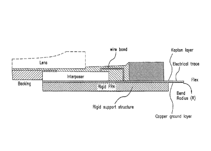
Referring now to FIG.5A, a schematic top plan view of an exemplary circuit
board for
mounting the transducer of the present invention thereto is illustrated. In
one aspect, at least a
portion of the circuit board can be flexible. In one embodiment, the circuit
board comprising a
bottom copper ground layer and a KaptonTm layer mounted to the upper surface
of the bottom
copper ground layer. In one aspect, the circuit board can also comprise a
plurality of underlying
substantially rigid support structures. In this aspect, a central portion
surrounding a central
opening in the circuit board can have a rigid support structure mounted to the
bottom surface of
the bottom copper ground layer. In a further aspect, portions of the circuit
board to which the
connectors can be attached also have rigid support structures mounted to the
bottom surface of
the bottom copper ground layer.
The circuit board further comprise a plurality of board electrical traces
formed thereon the
top surface of the KaptonTM layer, each board electrical trace having a
proximal end adapted to
couple to an electrical trace of the transducer and a distal end adapted to
couple to a connector,
-19-
CA 02935422 2016-07-06
such as, for example, a cable for communication of signals therethrough. In
one aspect, the
length of the circuit forming each electrical trace has a substantially
constant impedance.
The circuit board also comprises a plurality of vias that pass though the
KaptonTM layer
and are in communication with the underlying ground layer so that signal
return paths, or signal
ground paths, can be formed. Further, the circuit board comprises a plurality
of ground pins.
Each ground pin has a proximal end that is coupled to the ground layer of the
circuit board
(passing through one of the vias in the Kapton layer) and a distal end that is
adapted to couple to
the connector.
FIG. 5B is a top plan view of an exemplary circuit board for mounting of an
exemplary
256-element array having a 75 micron pitch and FIG. 5C is a top plan view of
the vias of the
circuit board of FIG. 5B that are in communication with an underlying ground
layer of the circuit
board. FIG. 5B also defines bores in the circuit board that are sized and
shaped to accept pins of
the connectors such that, when the connector is mounted thereon portions of
the circuit board,
there will be correct registration of the respective electrical traces and
ground pins with the
connector.
FIG. 6 illustrates a partial enlarged top plan view of a portion of the
exemplified circuit
board showing, in Region A, the ground electrode layer of the transducer being
wire bonded to an
electrical trace on the interposer, which can be, in turn, wire bonded to
ground pads of the circuit
board. The ground pads of the circuit board are in communication, through vias
in the ICaptonlm
layer, with the underlying bottom copper ground layer. As illustrated, in
Region B, the individual
electrical traces of the transducer are wire bonded to individual board
electrical traces of the
circuit board. Referring now to FIG.8A, in one aspect the central opening of
the circuit board
underlies the backing material of the transducer. FIG.7A is an enlarged
partial view Region B of
an exemplified transducer mounted to a portion of the circuit board.
Referring now to FIGS. 11A-11B, a transducer mounting is shown that does not
include
an interposer to the substantially rigid central portion of the circuit board.
This embodiment
allows for the elimination of most of the wire bonds. In this aspect, the PZT
stack is surface
mounted onto the circuit board directly by, for example, means of a series of
gold ball bumps.
The gold ball bump means is a conventional surface mounting technique and
represents another
type of surface mounting techniques consistent with the previously mentioned
surface mounting
techniques. In this example, the rigidized central portion of the circuit
board can provide the
same functionality as the interposer. Wire bonds, or other electrical
connection, from the ground
electrode of the PZT stack to the ground of the circuit board are still
required to compete the
- 20 -
CA 02935422 2016-07-06
signal return of the assembled device. FIG.11A shows the ground electrode
layer of the
transducer (without interposer) wire bonded to the ground pads of the circuit
board.
In one aspect, the gold ball bumps are applied directly onto the circuit
board. Each ball
bump is positioned in communication with one electrical trace of the circuit
board. When the
PZT stack is applied, it is aligned with the electrical traces of the circuit
board and electrical
continuity is made via the ball bumps. The PZT stack is secured to the circuit
board by, for
example and not meant to be limiting, a) use of an underfill, such as a UV
curable; b) use of an
ACF tape; c) by electroplating pure Indium solder onto the electrodes of
either the PZT or the
circuit board and reflovving the Indium to provide a solder joint between the
signal electrode on
the PZT and the gold ball bump on the circuit board, and the like.
An arrayed transducer can be operatively connected to the processing unit of
the system
using the flex circuit as shown in FIGS. 2A-11. Referring now to FIGS. 12-15,
the flex circuit
can be operatively connected with a BTH connector. BTH connectors are corrunon
and are
available in a variety of sizes. The BTH connector comprises a number of pins
for mating with a
BSH connector. The number of pins can be at least one greater than the number
of array
elements or traces of flex. For example, the number pins can be equal twice
the number of array
elements or corresponding traces of flex. Thus, in one example, 2x180 ¨ 360
pins can be used
for the 256 traces on the flex circuit of a 256 element array. In another
example, 256 pins can be
used for the exemplary 256 element array. The BSH connector can be
connectively seated within
.. the BTH. The BSH connector is operatively connected with an interface such
as a printed circuit
board that is terminated with a plurality of coaxial cables. A larger common
cable formed from
the plurality of coaxial cables can be terminated with a LIP end for
interfacing with the
processing unit of the ultrasound system at a ZIT receptacle or interfacing
site. One exemplary
ZW connector that can be used is a 360 Pin DLM6 ITT Cannon Zdrm connector as
available
from ITT Corporation of White Plains, NY. As would be clear to one skilled in
the art, however,
alternative ZIFilvl connectors can be used for interfacing with the processing
unit and can have
more or less than 360 pins.
The connection can comprise a cable or bundle of cables. The cable can connect
each
element of the array to the processing unit in a one-to-one relationship; that
is, each element can
be electrically connected with its own signal and a ground lead to a
designated connection point
in the processing unit whereby the plurality of individual element connections
are bundled
together to form the overall cable. Optionally, each individual electrical
connection can be
unbundled and not physically formed into a cable or cable assembly.
- 21 -
CA 02935422 2016-07-06
Suitable cables can be coaxial cables, twisted pairs, and copper alloy wiring.
Other
connection means can be via non-physically connected methods such as RF links,
infrared links,
and similar technologies where appropriate transmitting and receiving
components are included.
The individual element connections can comprise coaxial cable of a type
typically used
for connection array elements to processing units. These coaxial cables can be
of a low loss type.
The coaxial cables typically comprise a center conductor and some type of
outer shielding
insulated from the center conductor and encased in an outer layer of
insulation. These coaxial
cables can have nominal impedanees appropriate for use with an array. Example
nominal
impedances can be 50 ohms or more, including 50 ohms, 52 ohms, 73 ohms, 75
ohms or 80
ohms.
An exemplary medical cable for use with one or more of the ultrasound imaging
systems
described herein comprises a minimum of 256 coaxial cables of 40 AWG with a
nominal
impedance of about 75 ohms with coaxial cable lengths of about 2.0m. The
length can be less
than 2.0m or greater than 2.0m. The medical cable jacket length can
accommodate the cable
length, can include additional metal sheaths for electrical shielding and can
be made of PVC or
other flexible materials.
Cables and the connections for connecting an array transducer to the
processing unit,
including those described herein can be fabricated by companies such as
Precision Interconnect ¨
Tyco Electronics (Tyco Electronics Corporation, Wilmington, Delaware).
The exemplary cable, at the proximal end, can further comprise of flex/strain
relief, 12
PCBs interfacing between the coaxial cables and the ZIFI'm pins, a 360 Pin ITT
Cannon L11,114
connector and actuation handle (DLM6-360 type), and a shielded casing around
the connector.
The exemplary cable, at the distal end, can comprise of a flex/strain relief
cable terminated to two
PCBs, interfacing between the coaxial cables and the flex circuit board,
wherein each PCB has 1
BSH-090-01-L-D-A Samtec Connector (Samtec, Inc., New Albany, IN) and each PCB
has 75
Ohm characteristic impedance traces with cables terminated from both sides of
the PCB in a
staggered layout.
The cable can use a "flex circuit" method of securing and connecting a
plurality of coax
cables which comprise the large cable. In an exemplary embodiment, the array
has 256-elements.
The array is mounted in the central region of a flex circuit. The flex circuit
has two ends such
that the odd numbered elements 1,3,5,7...255 are terminated on the left end of
the flex with a
BTH-090 connector labeled J1, and that the even numbered elements
2,4,6,8...256 are terminated
on the right end of the flex with a BTH-090 connector labeled J3. For both
ends, the elements
- 22 -
CA 02935422 2016-07-06
are terminated in sequence along the upper and bottom rows of their respective
connectors with
GND (signal return) pins evenly dispersed across the connector in a repeated
pattern.
The repeat pattern is defined from the outer edge of the flex towards the
central region
of the flex and is as follows:
2 signal pins, GND
3 signal pins, GND
2 signal pins, GND
3 signal pins....
GND
3 signal pins, GND
2 signal pins, GND =
2 signal pins, GND.
A schematic showing a side view of the folded flex circuit, with the array
mounted in the
central array of the flex is shown in FIG.12A and an associated pin out table
for the connectors
on the flex circuit is shown in FIG 12B.
The flex circuit can be connected to the exemplary cable described above. The
flex
circuit can be connected to a Precision Interconnect ¨Tyco Electronics medical
cable assembly.
The electrical, for example, connection from the flex to the /.IF TM connector
can be made through
two scanhead PCBs followed by a coax cable bundle and 12 short PCBs each with
a 2x15
connector inserted into ZIFTM pins.
Each scanhead PCB (total of two) can comprise one BSH-090 connector, 128
traces (all
traces with controlled impedance of for example 75 Ohms at 30 MHz) and can be
terminated
with 128 (40 AWG 75 Ohm) coax cables. The PCB can have outer dimensions of
0.525" by
2.344."
FIG. 13 illustrates the design of the two scanhead PCBs. FIG 14 illustrates
how the PCBs
can be connected to the flex circuit and illustrates the staggered nature of
how the coax cable
ribbons can be soldered to the PCB. There are two scanhead PCBs. The left
board can be
connected to the J1 connector on the flex and the right board can be connected
to the 73
connector. EA ch scanhead PCB can have one BSH-090 connector. The pin-out for
each scanhead
trace can be matched to the pin out for the J1 and J3 connector.
ZIP Connector
An exemplary medical cable, as partially shown in FIG. 15A, comprises a ZIP
connector
on the proximal end, the end of the cable which connects to the processing
unit. One skilled in -
the art will appreciate that several designs of cable assemblies are possible.
FIG. 15B illustrates a
- 23 -
CA 02935422 2016-07-06
pin out that can be used for the exemplary HT Connector. The pins labeled as G
are signal return
pins. The pins labeled as N/C are not terminated with coaxial cables and these
pins are reserved
to be used as either for shielding to chassis ground or for other unspecified
functions. The N/C
pins can be accessible by simply removing the ZIF housing and soldering to the
unused traces on
any of the 12 PCBs connected to the ZIF.
The 12 individual PCBs used to connect to the LIP connector have coax cables
connected
on one or both sides of the board. One edge of the PCB can have a connector
suitable for
insertion into the ZIF connector (Samtec SSW or equivalent) and each PCB shall
have the
appropriate traces and vias required to connect the correct coaxial cable to
the correct Zit, pin.
Each PCB can have a Samtec SSW, or equivalent, connector with two rows of 15
pins, although
the number of coax cables may differ on some of the 12 PCBs as defined in the
Fig 15B. The
general layout of the pins on the 2x15 connector is universal and is shown in
Table 1.
One of the 12 PCBs requires provisions in the trace layout to include an
EEPROM as
defined in Fig 15B. Two of the 12 PCBs require some of the pins to be
terminated as required to
provide the hard-coded PROBE ID number that will identify the particular array
design included
inside the array assembly.
Various connection methods can be used including connectors of various styles.
For
these various connection methods, the impedance can be 75 Ohms at a center
frequency of 30
MHz.
-24 -
CA 02935422 2016-07-06
Table 1
The layout of connections on the connector end of the ZIP PCB that plugs into
the ITT
Connector.
General Pattern
Signal Signal
Signal GND
Signal Signal
GND Signal
Signal Signal
Signal Signal
Signal GND
Signal Signal
GND Signal
Signal Signal
Signal Signal
Signal GND
Signal Signal
GND Signal
Signal Signal
ULTRASOUND SYSTEM
An exemplary embodiment of an ultrasound system 1600 according to the present
invention is shown in FIG. 16. FIG. 16 is a block diagram illustrating an
exemplary high
frequency ultrasonic imaging system 1600. The blocks shown in the various
Figures can be
functional representations of processes that take place within an embodiment
of the system 1600.
In practice, however, the functions may be carried out across several
locations or modules within
the system 1600.
The exemplary system 1600 comprises an array transducer 1601, a cable 1619,
and a
processing unit 1620. The cable 1619 connects the processing unit 1620 and the
array transducer
1601. The processing unit may comprise software and hardware components. The
processing
unit can comprise one or more of a multiplexer(MUX)/front end electronics
1602, a receive
beamformer 1603, a beamformer control 1604, a transmit beamformer 1605, a
system control
1606, a user interface 1607, a scan converter 1608, a video processing display
unit 1609, and
processing modules including one or more of a M-mode processing module (not
shown), a PW
Doppler processing module 1611, a B-mode processing module 1612, a color flow
processing
module 1613, a 3-D mode processing module (not shown), and a RP mode
processing module
1615. The center frequency range of the exemplary system can be about 15-55
MHz or higher.
When measured from the outside edge of the bandwidths, the frequency range of
the exemplary
system can be about 10-80 MI-lz or higher.
The array transducer 1601 interfaces with the processing unit 1620 at the
MUX/front end
- 25 -
CA 02935422 2016-07-06
electronics (MUX/FEE) 1602. The MUX portion of the MUX/FEE 1602 is a
multiplexer which
can electronically switch or connect a plurality of electrical paths to a
lesser number of electrical
paths. The array transducer 1601 converts electrical energy to ultrasound
energy and vice versa
and is electrically connected to the MUX/FEE 1602.
The MUX/FEE 1602 comprises electronics which generate a transmit waveform
which is
connected to a certain subset of the elements of the array, namely the
elements of the active
aperture. The subset of elements is called the active aperture of the array
transducer 1601. The
electronics of the MUX/FEE 1602 also connects the active aperture of the array
to the receive
channel electronics. During operation, the active aperture moves about the
array transducer 1601,
in a manner determined by components described herein.
The MUX/FEE 1602 switchably connects the elements of the active aperture to
transmit
and receive channels of the exemplary system. In an exemplary 256-element
array transducer
embodiment of the invention, there are 64 transmit channels and 64 receive
channels that can be
switchably connected to the active aperture of up to 64 elements. The up to 64
elements of the
active aperture are contiguous. In certain embodiments of the invention, there
is a separate
transmit MUX and a separate receive MUX. Other embodiments of the invention
share the MUX
for both the transmit channels and the receive channels.
During a transmit cycle of the exemplary ultrasound system 1600, the front end
electronics portion of the MUX/FEE 1602 supply a high voltage signal to the
elements of the
active aperture of the array transducer 1601. In one aspect, the front end
electronics can also
provide protection circuitry for the receiver channels to protect them from
the high voltage
transmit signal, as the receive channels and the transmit channels have a
common connection
point at the elements of the array transducer 1601. The protection can be in
the form of isolation
circuitry which limits the amount of transmit signal that can leak or pass
into the receive channel
to a safe level which will not cause damage to the receive electronics.
Characteristics of the
MUX/FEE 1602 include a fast rise time on the transmit side, and high bandwidth
on the transmit
and receive channels.
The MUX/FEE 1602 passes signals from the transmit beamformer 1605 to the array
transducer 1601. In an exemplary embodiment, the transmit bearnformer 1605
generates and
supplies separate waveforms to each of the elements of the active aperture. In
an exemplary
embodiment, the waveform for each element of the active aperture is the same.
In another aspect,
the waveforms for each element of the active aperture are not all the same and
in some
embodiments have differing center frequencies.
-26 -
CA 02935422 2016-07-06
hi one exemplary embodiment, each separate transmit waveform has a delay
associated
with it. The distribution of the delays for each element's waveform is called
a delay profile. The
delay profile is calculated in a way to cause the desired focusing of the
transmit acoustic beam to
the desired focal point. In certain embodiments, the transmit acoustic beam
axis is perpendicular
to the plane of the array 1601, and the beam axis intersects the array 1601 at
the center of the
active aperture of the array transducer 1601. The delay profile can also steer
the beam so that it is
not perpendicular to the plane of the array 1601. In an exemplary aspect of
the present invention,
a delay resolution of 1/16 can be used. Or, in other words, 1/16 of the period
of the center
frequency of the transmit center frequency, though other delay resolutions are
contemplated
within the scope of this invention. For example at a 50 MHz center frequency,
the period is 20
nanoseconds, so 1/16 of that period is 1.25 nanoseconds, which is the
exemplary delay resolution
used to focus the acoustic beam. It is to be appreciated that the delay
resolution may be different
than 1/16th of a period, for example delay resolutions less than 1/16th (e.g.,
1/24, 1/32, etc) as well
as delay resolutions greater than 1/16 (e.g., 1/12, 1/8, etc.) are
contemplated within the scope of
this invention.
The receive beamformer 1603, can also be connected to elements of the active
aperture of
the array transducer 101 via the MUX/FEE 1602. During transmit an acoustic
signal penetrates
into the subject and generates a reflected signal from the tissues of the
subject. The reflected
signal is received by the elements of the active aperture of the array
transducer 1601 and
converted into an analog electrical signal emanating from each element of the
active aperture.
The electrical signal is sampled to convert it from an analog to a digital
signal in the receive
beamformer 1603. Embodiments of the invention use quadrature sampling for
digitization of the
received signal. During the receive cycle of the system 1600, the array
transducer 1601 also has a
receive aperture that is determined by the beamformer control 1604, which
tells the receive
beamformer 1603 which elements of the array to include in the active aperture
and what delay
profile to use. The receive beamformer 1603 of the exemplary embodiment is a
digital
beamformer.
The receive beamformer 1603 introduces delays into the received signal of each
element
of the active aperture. The delays are collectively called the delay profile.
The receive delay
profile can be dynamically adjusted based on time¨of-flight ¨ that is, the
length of time that has
elapsed during the transmission of the ultrasound into the tissue being
imaged. The time-of-flight
is used to focus the receive beamformer to a point of focus within the tissue.
In other words, the
depth of the receive beam is adjusted using a delay profile which incorporates
information
- 27 -
CA 02935422 2016-07-06
pertaining to the time-of-flight of the transmitted beam.
The received signal from each element of the active aperture is summed wherein
the sum
incorporates the delay profile. The summed received signal flows along the
receive channel from
the receive beamformer 1603 to one or more of the processing module(s) 1611,
1612, 1613,
and/or 1615, including those not shown in FIG. 16), as selected by the user
interface 1607 and
system controls 1606, which act based upon a user input.
The beamformer control 1604 is connected to the MUX/FEE 1602 through the
transmit
beamformer 1605 and the receive beamformer 1603. It is also connected to the
system control
1606. The beamformer control 1604 provides information to the MUXJFEE 1602 so
that the
desired elements of the array transducer 1601 are connected to form the active
aperture. The
beamformer control 1604 also creates and sends to the receive beamformer 1603
the delay profile
for use with the reception of a particular beam. In embodiments of the
invention, the receive
delay profile can be updated repeatedly based upon the time of flight. The
beamformer control
1604 also creates and sends to the transmit beamformer 1605 the transmit delay
profile.
The system control 1606 operates in a manner known to one of ordinary skill in
the art. It
takes input from the user interface 1607 and provides the control information
to the various
components of the system 1600 in order to configure the system 1600 for a
chosen mode of
operation. The scan converter 1608 operates in a manner known in the art and
takes the raw
image data generated from the one or more of the processing modules and
converts the raw image
data into an image that can be displayed by the video processing/display 1609.
For some
processing modes of operation, the image can be displayed without using the
scan converter 1608
if the video characteristics of the image are the same as those of the
display.
The processing modules, except as noted herein, function in a manner known to
one of
ordinary skill in the art. For the PW Doppler module 1611 and the color flow
processing module
1613, the pulse repetition frequency (PRF) can be high due to the high center
frequencies of
embodiments of this invention. The maximum unaliased velocities which may be
measured are
proportional to the PRF and inversely proportional to the transmit center
frequency. The PRFs
required to allow for the unaliased measurement of specific velocities given
specific transmit
center frequencies may be calculated in a method known to one of ordinary
skill in the art. Given
that the transmit center frequencies used are in the range of 15 to 55MHz, or
higher, and the
blood flow velocities can be as high as 1 in/s and in some cases greater than
1 m/s unaliased
measurement of the Doppler signal resulting from those velocities will require
the PRF for PW
Doppler to be up to 150KHz. Embodiments of the invention have a PW Doppler
mode which
-28 -
CA 02935422 2016-07-06
supports PRFs up to 150 ICHz, which for a center frequency of 30 MHz allows
for unaliased
measurement of blood velocities up to 1.9 rn/s in mice with a zero degree
angle between the
velocity vector of the moving target and the ultrasound beam axis.
In certain embodiments, the RF module 1615 uses interpolation. If the sampling
method
used is quadrature sampling, then the RF signal may be reconstructed from the
quadrature
baseband samples by zero padding and filtering, as would be known to one of
ordinary skill in
the art. If Nyquist sampling is used, then no reconstruction is required since
the RF signal is
sampled directly. In certain embodiments, the RF module 1615 reconstructs the
RF signal from
the quadrature samples of the receive beamformer output. The sampling takes
place at the center
frequency of the receive signal, but in quadrature, giving a baseband
quadrature representation of
the signal. The RF signal is created by first zero padding the quadrature
sampled data stream,
with the number of zeros determined by the desired interpolated signal sample
rate. Then, a
complex bandpass filter is applied to the zero padded data stream, which
rejects the frequency
content of the zero padded signal that is outside the frequency band from fs/2
to 3fs/2, where fs is
the sample frequency. The result after filtering is a complex representation
of the original RF
signal. The RF signal is then passed on to the main computer unit for further
processing such as
digital filtering and envelope detection and display. The real part or the
complex representation
of the RF signal may be displayed. For example, the RF data acquired for a
particular scan line
may be processed and displayed. Alternatively, RF data from a certain scan
line averaged over a
number of pulse echo returns can be displayed, or RF data acquired from a
number of different
scan lines can be averaged and displayed. The scan lines to be used for
acquisition of the RF data
can be specified by the user based on evaluation of the B-Mode image, by
placing cursor lines
overlaid on the B-Mode image. A Fast Fourier Transform (FFT) of the RF data
can also be
calculated and displayed. The acquisition of RF data and the acquisition of B-
Mode data can be
interleaved so as to allow for the display of information from both modes
concurrently in real
time. The acquisition of physiological signals such as te ECG signal can also
occur
concurrently with the acquisition of RF data. The ECG waveform can be
displayed while the RF
data is acquired. The timing of the acquisition of RF data can be synchronized
with user defined
points within the ECG waveform, thereby allowing for the RF data to be
referenced to specific
times during a cardiac cycle. The RF data can be stored for processing and
evaluation at a later
time.
FIG. 17 shows a block diagram of the system 1600 further illustrating
components of an
embodiment of the invention. The array transducer 1601 is connected to the
front end
-29-
CA 02935422 2016-07-06
transformer 1702 via a cable 1619. The cable 1619 comprises signal pathways
from the elements
of the array transducer 1601 to the front end transformers 1702. An exemplary
embodiment of
the cable is described herein and comprises individual micro-coax cables. In
addition, connectors
can be used on one or both ends of the cable 1619. In one aspect of the
invention, a connector
with pins equal to twice th3 number of elements can be used and an exemplary
connector is
described herein. For each element of the array transducer 1601 a signal and a
ground path can
be used. In other embodiments of the invention, the ground connection is
shared for a grouping
of elements. . Alternatively, the MUX/Front End Electronics 1702, 1703, 1704,
1708 can be
located inside the housing for the linear transducer array 1601
FIG. 17 provides representative details of the circuitry for four elements of
the array
transducer 1601 as examples for the larger system 1600 wherein there is a
front end transformer
1702 and transmit output stage 1703 for each element. For an embodiment with a
256 element
array transducer 1601, there are 256 front end transformers 1702 and transmit
output stages 1703.
The front end transformers 1702 and transmit output stages 1703 are more fully
described below.
During receive, the electrical signal from an element of the array transducer
1601 passes through
the front end transformer 1702 into the receive multiplexer 1704. The receive
multiplexer 1704
selects which element and front end transformer are connected to the receive
channel 1705. The
receive channel 1705 comprises a low noise amplifier and a time gain control,
both more fully
described below. The signal then passes from the receive channel 1705 into the
analog-to-digital
conversion 1706 module where it is digitized. The digital received signal then
passes into the
receive beamformer 1707, which is a digital beamformer. In block 1707, a delay
profile
generated in the beamformer control is applied to the received signal. The
signal from the
received beamformer 1707 travels into the synthetic aperture memory 1710. The
synthetic
aperture memory adds the received data from two successive ultrasound lines.
An ultrasound line
is considered to be the data resulting from returning ultrasound echoes that
is received after the
transmission of an ultrasound pulse into tissue. Synthetic aperture imaging
performs as one of
ordinary skill in the art would understand. In part, synthetic aperture
imaging refers to a method
of increasing the effective size of the transmit or receive aperture. . For
example, if there are 64
channels in the beamformer, during the reception of one line of ultrasound
data, up to 64 transmit
channels and 64 receive channels can be used. Synthetic aperture imaging will
use two lines of
ultrasound data, added together. The first ultrasound line can be acquired
with a receive aperture
which can span elements 33 to 96. The second ultrasound line is received with
an aperture
segmented into two blocks, located at elements 1 to 32 and 97 to 128. Both
ultrasound lines use
- 30 -
CA 02935422 2016-07-06
the same transmit aperture. When the 2 ultrasound lines are summed, the
resulting ultrasound line
is essentially the same as that which would have been received had the receive
aperture consisted
of 128 channels located at elements Ito 128, provided that there is no
appreciable motion of the
tissue being imaged during the time required to acquire the two lines of
ultrasound data. In this
instance two ultrasound lines were required rather than just one, so the frame
rate is lowered by a
factor of two. The two receive apertures can be arranged in a different way,
as long as together
they form a 128 element aperture. Alternatively, the transmit aperture size
can be increased while
keeping the receive aperture the same. More than 2 ultrasound lines can be
used to increase the
aperture by more than a factor of two. The signal from the synthetic aperture
niemory 1710 is
then stored in the RF eine buffer 1713, which is a large memory that sores
many received RF
lines, as controlled by the asynchronous processing control module 1714. The
buffered receive
signal is then read into the signal processing unit 1715 at an appropriate
rate. The signal
processing unit 1715 may be implemented with a dedicated CPU on the beamformer
control
board. The received signal passes from the signal processing unit 1715 to the
computer unit 1717
where it is further processed according to the mode selected by the user. The
processing of the
received signal by the computer unit 1717 is generally of the type known to a
person of ordinary
skill in the art, with exceptions as noted herein.
In one embodiment, as shown in FIG. 17, the computer unit 1717 comprises
system
software configured to process signals according to the operation mode of the
system. For
example, the system software in the main computer unit 1717 may be configured
to carry out B-
Mode processes which may include, for example, preprocessing; persistence
processing; cineloop
image buffer; scan conversion; image pan; zoom and postprocessing. The system
software in the
main computer unit 1717 may also be configured to carry out processes for
color flow imaging
(CFI), which may include, for example, threshold decision matrix; estimate
filtering; persistence
and frame averaging; cineloop CFI image buffer; scan conversion; color maps
and priority. The
system software in the main computer unit 1717 may also be configured to carry
out processes
for PW Doppler, which may include, for example spectral estimation (FFT);
estimate filtering;
cineloop spectral data buffer; spectral display generation; postprocessing and
dynamic range and
audio processing.
The embodiment of the system of FIG. 17 is also comprised of a user interface
panel
1720. In this embodiment the user interface panel 1720 is similar to the
standard user interface
found on most clinical ultrasound systems. For example, the B-Mode user
interface may have
image format controls that include image depth; image size; dual image
activate; dual image
- 31 -
CA 02935422 2016-07-06
left/right select; flip image left/right; flip image up/down and zoom.
Transmit controls may
include transmit power (transmit amplitude); transmit focal zone location;
number of transmit
zones selection; transmit frequency and number of cycles. Image optimization
controls may
include; B-Mode Gain; TGC sliders; preprocessing; persistence; dynamic range;
frame
rate/resolution control and post-processing curves.
As another example of mode-dependent interface controls, a color flow imaging
user
interface may have image format controls that may include color flow mode
select (e.g., color
flow velocity, Power Doppler, Tissue Doppler); trackball; steering angle;
color box position/size
select (after selection trackball is used to adjust position or size); preset
recall; preset menu and
invert color map. Transmit controls may include transmit power (transmit
amplitude); transmit
focal zone location and transmit frequency. Image optimization controls may
include; color flow
gain; gate size; PRF (alters velocity scale); clutter filter select; frame
rate/resolution control;
preprocessing select; persistence; dynamic range (for Power Doppler only) and
color map select.
Yet another example of a user interface is a PW Doppler user interface which
may have
PW Doppler format controls that may include PW Doppler mode select; trackball;
activate PW
cursor (trackball is used to adjust sample volume position); sample volume
size; Doppler steering
angle; sweep speed; update (selects either simultaneous or interval update
imaging); audio
volume control and flow vector angle. Transmit controls may include transmit
power (transmit
amplitude) and transmit frequency. Spectral Display optimization controls may
include PW
Doppler gain; spectral display size; PRF (alters velocity scale); clutter
filter select; preprocessing
and dynamic range.
An exemplary M-Mode user interface may have image format controls including M-
Mode
cursor activation; trackball (used to position cursor); strip size and sweep
speed. Transmit
controls may include transmit power (transmit amplitude); transmit focal zone
location; transmit
frequency and number of cycles. Image optimization controls may include M-Mode
gain;
preprocessing; dynamic range and post-processing.
An exemplary RE Mode user interface may have, for example, RF line acquisition
controls that may include RF line position; RF gate; number of RF lines
acquired; RF region
activate; RF region location; RF region size; number of RF lines in region;
averaging; and B-
Mode interleave disable. Transmit controls may include transmit power
(transmit amplitude);
transmit focal zone location; transmit f-number; transmit frequency, number of
cycles;
acquisition PRF and steering angle. Receive processing controls may include RF
Mode gain;
filter type, order, window type and number of lines averaged.
- 32 -
CA 02935422 2016-07-06
The digital samples of the received signal are processed at a rate which is
generally
different from the rate at which the data is acquired. Such processing is
referred to herein as
"asynchronous signal processing." The processing rate is the rate at which
data is displayed,
typically about 30 frames per second (fps.) As one would recognize, however,
the data can be
displayed at a rate up to the acquisition rate or can be displayed at less
than about 30 fps. The
data can be acquired at much faster frame rates, in certain embodiments of the
invention at about
300 frames per second, or at a speed necessary to acquire the diagnostic
information desired. For
example, image date of a rapidly moving anatomical structures such as a heart
valve can be
acquired using a faster frame rate and then can be displayed at a slower frame
rate. Data
acquisition rates can be less than 30 fps, 30 fps, or more than 30fps. For
example, data
acquisition rates can be 50, 100, 200, or 300 or more fps.
The display rate can be set such that it does not exceed that which the human
eye can
process. Some of the frames which can be acquired can be skipped during
display, although all
of the data from the receive beamformer output is stored in an RF data buffer
such as the RF cine
buffer 1713. The data is sometimes referred to as RF data or by the sampling
method used to
acquire the data, (for instance in the case of quadrature sampling, the data
can also be referred to
as baseband quadrature data). The quadrature or RF data is processed prior to
display. The
processing may be computationally intensive, so there are advantages to
reducing the amount of
processing used, which is accomplished by processing only the frames which are
to be displayed
at the display rate, not the acquisition rate. The frames that were skipped
over during display can
be viewed when live imaging stops or the system is "frozen." The frames in the
RF buffer 1713
can be retrieved, processed, and played back at a slower rate, e.g., if the
acquisition rate is 300
frames per second, the play back of every frame at 30 frames per second would
be 10 times
slower than normal, but would allow the operator to view rapid changes in the
image. The
playback feature is usually referred to as the "Cineloop" feature by persons
of ordinary skill in the
art. Images can be played back at various rates, or frame by frame, backwards
and forwards.
The system 1600 shown in FIG. 17 can also comprise various items which one of
ordinary
skill in the art would recognize as being desirable for the function of the
system, such as clocks
1712, memory, sound card and speakers, video card and display, etc. and other
functional blocks
as shown in FIG. 17.
FIGS. 18a and 18b provide additional detail of an embodiment of the MUX/Front
End
Electronics 1702, 1703, 1704, 1708 and, the receive beamformer 1707 and
transmit beamformer
1709 functions according to an embodiment of the present invention. In the
embodiment shown
- 33 -
CA 02935422 2016-07-06
in FIG. 18a, a channel, for instance a receive channel, can be connected to a
node and that node is
connected to, for example, four (4) elements of the array transducer 1601
through a switching
circuit, or multiplexing circuit, as shown in FIG. 18a. For instance, channel
1 1801 may be
switchably connected to elements numbered 1, 65, 129, and 193 in FIG. 18a so
that only one of
those four elements are connected to channel 1 1801 at any given time. This,
in essence, is the
performance of the multiplexing function of the MUX/Front End Electronics
1702, 1703, 1704,
1708 during the receive cycle of the system 1600. The assignment of four
switchably connected
elements to a channel is done such that contiguous elements of any given
subset of elements can
comprise the active aperture. For example, if the array transducer were
comprised of 256
elements, then 64 or less elements can form the subset that comprises the
active aperture.
The multiplexing of the elements of the array transducer 1601 for the receive
cycle can be
carried out by a RX switch 1817 as shown in an exemplary diagram (FIG. 18b) of
the front end
1802. A control signal 1818 from the beamformer control 1711 determines which
RX switch
1817 is activated, thereby connecting the chosen element of the four (4)
available elements for
that module 1802 to the receive channel. As one skilled in the art would
appreciate, the
multiplexing scheme illustrated in FIGS. 18a and 18b can be applied to
transducers of varying
numbers of elements (other than 256 elements) and of varying maximum active
aperture sizes
(other than up to 64 elements).
The exemplary front end 1816 shown in FIG. 18b also comprises the transformer
1819
and pulser 1820, which are described in more detail below. In one aspect, the
front end 1816
provides isolation of the receive channel from the transmit waveform,
discussed previously
herein.
The received signal from the selected array transducer element passes into the
low noise
amplifier (LNA) 1804. From the LNA 1804, the then amplified signal passes into
time gain
control (TGC) 1805. Since elapsed time is proportional to the depth of the
received reflected
signals, this is also referred to as a depth dependent gain control. In an
ultrasound system, as
time goes by from the transmission of an ultrasound wave, the signal passes
deeper into the tissue
and is increasingly attenuated; the reflected signal also suffers this
attenuation. The TGC 1805
amplifies the received signal according to a time varying function in order to
compensate for this
attenuation. The factors which can be used to determine the time varying TGC
gain are time of
flight, tissue characteristics of the subject or subject tissue under study,
and the application (e.g.
imaging modality). The user may also specify gain as a function of depth by
adjusting TGC
controls on the user interface panel 1607. Embodiments may use, for example,
an Analog
= - 34 -
CA 02935422 2016-07-06
Devices (Norwood, MA) AD8332 or similar device to perform the LNA 1804 and TGC
1805
functions. From the TGC 1805, the receive signal passes into the receive
beamformer 1803
where it is sampled by a sampler, in this embodiment, the analog-to-digital
converters 1807 and
1808. In other embodiments according to the invention only one analog-to-
digital converter is
.. used if sampling is done at a rate greater than the Nyquist rate; for
instance at 2 or 3 times the
Nyquist rate, where the Nyquist rate involves sampling the ultrasound signals
from the individual
elements at a rate which is at least twice as high as the highest frequency in
the signal.
In other embodiments of the invention, quadrature sampling is employed and two
analog-
to-digital converters are used, namely the "I' and the "Q" sampler. In the
exemplary embodiment
of the receive beamformer 1803, the receive signal is digitized in blocks 1807
and 1808 using
quadrature sampling analog-to-digital converters (ADC); two ADCs are required
per channel,
with sampling clocks shifted 90 .out of phase. The sample rate used can be the
center frequency
of the receive signal. For comparison, direct sampling would use a sampling
rate in theory of at
least twice the highest frequency component in the receive signal, but
practically speaking at least
three times the sampling rate is preferred. Direct sampling would use one ADC
per channel.
Once sampled, the now digitized received signal passes into a Field
Programmable Gate
Array (FPGA) in which various functions associated with receive beamforming
are implemented.
Within the FPGA, the digitized received signal can undergo a correction for
the DC offset of the
ADC. This is implemented by the subtraction of a value equal to the measured
DC offset at the
ADC output. Each ADC may have a different DC offset correction value. The DC
offset may be
determined by averaging a number of digital samples appearing at the output of
the ADC with no
signal present at the receive channel input, for example, during a calibration
period at system start
up. The digitized signal next passes into a FIFO buffer 1822 where each sample
is stored for an
appropriate duration so that the appropriate delay profile can be implemented.
The delay can be
implemented in both coarse and fine manners. A coarse delay can be implemented
by shifting
the signal by one or more sample points to obtain the desired delay. For
instance, if the desired
delay is one sample period, then shifting by one sample in the appropriate
direction provides a
signal with the appropriate delay. However, if a delay of a value not equal to
the sample period is
desired, a fine delay can be implemented using an interpolation filter 1809.
From the FIFO buffer 1822, the digitized received signal passes into the
interpolation
filter 1809 for the calculation of any fine delay. The interpolation filter
1809 is used in a system
where the sample period is greater than the appropriate fine delay resolution.
For instance, if the
sample rate is the center frequency of the ultrasound signal and is 50 MHz,
the sample rate is one
- 35 -
CA 02935422 2016-07-06
sample every 20 nanoseconds. However, a delay resolution of 1.25 nanoseconds
(1/16 of 20
nanoseconds) is used in certain embodiments to provide the desired image
quality, though other
delay resolutions are contemplated within the scope of this invention. The
interpolation filter
1809 is used to calculate a value for the signal at points in time other than
the sampled point. The
.. interpolation filter 1809 is applied to the in-phase and quadrature
portions of the sampled signal.
Embodiments of the interpolation filter 1809 comprise a finite impulse
response (MR) filter. The
coefficients of each filter can be updated dynamically by the beamformer
control module based
on the time of flight, sample by sample. After processing by the interpolation
filter, a phase
rotation can be applied by a multiplier 1811 multiplying the in-phase and
quadrature components
by the appropriate coefficients. The phase rotation is used to incorporate
into the interpolated
sample the correct phase relative to the ADC sample frequency. The RX
controller 1810 controls
the FIFO modules and the interpolation filters. The receive delay is updated
dynamically, so the
interpolation filter coefficients at each channel need to change at certain
intervals. The delay
implemented by the FIFO also needs to change at certain intervals. Also, the
receive aperture
size is adjusted dynamically, so each channel becomes active at a specific
time during the
reception of the ultrasound signal; a channel is activated by multiplying by 1
instead of 0 at the
"multiply" module 1811. The multiply module 1811 can also apply a "weight"
which is a value
between 0 and 1, independently to each channel in the receive aperture. This
process, which is
known as apodization, is known to one skilled in the art. The value by which
the interpolated
sample is multiplied by may vary with time, so as to implement an apodized
receive aperture
which expands dynamically during the reception of the ultrasound signal.
FIG. 18c is an exemplary embodiment of a receive controller (RX controller) in
an
embodiment according to the present invention. The Receive Controller 1810 is
used to program
the correct delay profile, aperture size and receive apodization data into the
processing block
1809 which implements the interpolation and phase rotation and apodization.
The Receive
Controller 1810 of FIG. 18c sets the initial parameters (Initial Coarse Delay,
Initial Phase) once
per start-of-line (SOL) trigger and sets the dynamic parameters (Dynamic
Focus, Dynamic
Apodization) once per receive clock (RXCLK) period. The initial receive delay
profile is stored
in RX Initial Aperture Memory 1822. The dynamic receive delay profile is
stored in the RX
Dynamic Aperture Memory 1824. The delay profile is loaded into the RXBF Buffer
1826 via the
64:16 Crosspoint Switch 1828 before the SOL trigger. The crosspoint switch
1828 selects 16 of
the 64 aperture channel configurations. These are used to program the 16
receive channels that
are on a single Channel board.
-36-
CA 02935422 2016-07-06
The configuration for each receive line is stored in the Line Memory 1830.
Each line
configuration in the Line Memory 1830 contains the Aperture Select Index, the
Mode Select, and
the Aperture Enable. The Aperture Select index is used to determine the
Aperture to Channel
mapping. The Mode Select is used to access multiple delay profiles. The
Aperture Enable index
controls the initial aperture size. The aperture select look-up table (AP_SEL
LUT) 1832 is a
method to reduce the number of possible configurations and therefore number of
bits required to
store in the line memory. The AP_SEL LUT 1832 is re-programmable.
The Memory Control 1834 is a state machine that decodes the line
configuration. The
state machine is configured by the Control and Status memory 1836. It is
configured differently
for different modes (e.g. B-Mode, Color Flow Mode, PW Doppler Mode, etc.). The
Memory
Control 1834 controls the loading of the aperture memory into the RXBF Buffer
1826 and
generates the SOL_delayed and FIFO_WEN signals. The pulse SOL_delayed is used
to transfer
the initial delay parameters into the RX Phase Rotation and RX Apodization
block 1809 in a
single RXCLK period. The dynamic receive parameters are then transferred in
each subsequent
RXCLK period. The FIFO_WEN signal starts the receive ADC data acquisition into
the FIFO
for the RX interpolation filter.
The Control and Status Memory 1836 also contains common parameters such as the
Receive Length. The Receive Length parameter determines how many receive
samples to collect
for each line.
It is to be appreciated that increasing the number of receive channels allows
for larger
receive apertures, which can benefit deep imaging by improving lateral
resolution and
penetration. The synthetic aperture mode allows for apertures greater than 64
to be used, but at
the expense of a reduction in frame rate. With an increase in the number of
receive channels, this
can be done without a frame rate penalty.
In one embodiment according to the present invention, the receive beamformer
1803
allows for multi-line beamforming. Multi-line beamforming allows for higher
frame rates by
processing multiple receive lines in parallel. Frame rate increases by a
factor equal to the number
of parallel receive lines. Since beamforming occurs simultaneously for
multiple receive
apertures, higher data processing rates through the interpolation filters 1809
are used. The amount
of data transferred from the receive beamformer to a host CPU would increases
by a factor equal
to the number of parallel receive lines. The transmit beam is broadened so
that it overlaps the
multiple receive lines.
The signal from each receive beamformer 1803 is then summed by summers 1815.
The
-37-
CA 02935422 2016-07-06
summed signal represents a received signal at a given time that is reflected
from a given depth.
The summed received signal is then routed through modules described earlier
and shown in FIG.
17, to the appropriate processing module for the mode of operation selected by
the user.
During the transmit operation cycle of the system 1600, selected transmit
output stages
are connected to the transmit channel in order to form the active aperture. In
this aspect, the
multiplexing is done prior to the transmit output stage. For example, as
previously described,
transmit channel 1 1801 can be switchably connected to the transmit output
stages corresponding
to elements numbered 1, 65, 129, and 193 in FIGS. 18a and 18b so that only one
of those four
transmit output stages are connected to transmit channel 1 1801 at any given
time. It can also be
seen in FIGS. 18a and 18b that transmit channel 2 can be switchably connected
to the transmit
output stages corresponding to elements 2, 66, 130 and 194, and so on. This is
the performance
of the multiplexing function of the MUX/Front End Electronics 1702, 1703,
1704, 1708 during
the transmit cycle of the system.
Referring to FIG. 20, the transmit signal which is multiplexed is the pair of
signals
designated by TXA 2002 and TXB 2004, which drive the gates of the transmit
pulser MOSFETs
QTDN 2006 and QTDP 2008 as shown in FIG. 20. These signals 2002,2004 are
unipolar signals
of a sufficiently low level so that multiplexing by MOSFET type switches can
be used. The
assignment of four switchably connected transmit output stages to a transmit
channel is done
such that contiguous elements of any given subset of elements can comprise the
active transmit
aperture. For example, in an array transducer comprised of 256 elements, 64 or
less elements can
form the subset that comprises the active transmit aperture.
Optionally, the transmit multiplexing can be done after the transmit output
stage using
multiplexing circuitry able to accommodate a higher voltage bipolar signal.
Referring back to FIGS. 18a-18d, the transmit beamformer 1812 generates the
transmit
waveform with the specified delay present in the waveform in that the waveform
is not sent until
the appropriate time per the delay profile. The transmit waveform can be a low
voltage signal,
including a digital signal. Optionally the transmit waveform can be a high
voltage signal used by
the array transducer to convert electrical energy to ultrasound energy. The
operation of the
transformer 1819 and pulser 1820 are described in greater detail below.
During the process of transmit beamforming, one or more of each of the
transmit channels
within the active transmit aperture can produce a transmit waveform which can
be delayed
relative to a reference control signal. The number of transmit channels
determines the maximum
transmit aperture size. The benefit of increasing the number of transmit
channels is improved
- 38 -
CA 02935422 2016-07-06
lateral resolution and penetration for deep imaging. In various embodiments,
the array transducer
has 64 transmit channels or may have 96 or 128 transmit channels. The delays
can vary from
channel to channel, and collectively the delays are referred to as the
transmit delay profile.
Transmit beamforming may also include the application of a weighting function
to the transmit
waveforms, a process known to one of ordinary skill in the art as
"apodization." Transmit
apodization uses independent control of the amplitude of the transmitted
waveform at each
channel. The benefit to image quality is improved contrast resolution due to a
reduction in
spurious lobes in the receive beam profile, which can be either side lobes or
grating lobes. Each
transmitter output stage can have an independently controlled supply voltage,
and control
hardware.
Transmit waveshaping involves the generation of arbitrary waveforms as the
transmit
signal, e., the modulation of amplitude and phase within the transmit
waveform. The benefit is
an improvement to axial resolution through shaping of the transmit signal
spectrum. Techniques
such as coded excitation can be used to improve penetration without loss of
axial resolution.
The transmit beamformer 1812 described herein may be implemented in one
embodiment
with an FPGA device. A typical implementation of a transmit beamformer 1812
which provides
a delay resolution of, for example, 1/16 the transmit clock period may require
a clock which is 16
times the transmit clock frequency. For the frequency range of the system
described here, this
would imply a maximum clock frequency of 16 times 50 MHz, or 800 MHz, and a
typical FPGA
device may not support clock frequencies at that rate. However, the transmit
beamformer 1812
implementation described below uses a clock frequency within the FPGA of only
eight (8) times
the transmit clock frequency.
Each channel of the transmit beamformer is comprised of a TX controller 1814
and a Tx
pulse generator 1813. The TX controller 1814 uses a parameter called, for
example, an
ultrasound line number (also known as a ray number), to select the active
transmit aperture
through the appropriate configuration of the transmit multiplexer. The ray
number value
identifies the origin of the ultrasound scan line with respect to the physical
array. Based on the
ray number, a delay value is assigned to each transmit channel in the active
transmit aperture.
The TX pulse generator 1813 generates a transmit waveform for each transmit
channel using
waveform parameters and control signals as described herein.
FIG. 18d is an illustration of an exemplary transmit controller (TX
controller) in an
embodiment according to the present invention. The transmit controller 1814 is
used to program
the TX pulse generator 1813 with the correct delay profile (coarse delay and
fine delay for each
- 39 -
CA 02935422 2016-07-06
channel) and transmit waveform for each line. It re-programs the TX pulse
generator 1813 before
each line. The sequence of lines is used to produce a 2-D image. Each line
requires a certain
subset of the array elements to be used to form the transmit aperture. Each
array element within
the aperture must be connected to a channel in the TX pulse generator 1813,
and the transmit
channels must be configured to produce the desired transmit waveforms with
delays according to
the desired transmit delay profile.
The delay profile and transmit waveform for the entire aperture is stored in
the TX
Aperture Memory 1838. Multiple delay profiles can be stored in the TX Aperture
Memory 1838.
Multiple delay profiles are required for B-Mode imaging in which multiple
focal zones are used,
and PW Doppler and Color Flow Imaging modes in which the Doppler mode focal
depth and
transmit waveforms are different than those used for B-Mode. In this exemplary
embodiment,
the TX Aperture Memory 1838 contains delay profile and transmit pulse wave
shape data for a 64
channel aperture. On each Channel Board there are 16 transmit channels, each
of which can be
connected to one of four different array elements through a transmit output
stage. A 64:16
crosspoint switch 1840 is used to route the correct transmit waveform data
sets to each of the 16
channels. The control of the other 48 channels is implemented on the other 3
channel boards.
The TXBF buffer 1842 temporarily stores the TX pulse generator data before the
start of line
(SOL) trigger. The TX TRG trigger moves the data from the TXBF Buffer 1842
into the TX
Pulse generator 1813 in one TXCLK period.
The configuration for each transmit line is stored in the Line Memory 1844.
Each line
configuration in the Line Memory 1844 contains the following information:
Aperture Select
Index, Mode Select, Aperture Enable Index, and Element Select Index. The
Aperture Select
index is used to determine the Aperture to Channel mapping. The Mode Select is
used to access
multiple delay profiles. The Aperture Enable index controls the aperture size.
The Element
Select index controls which element is active in the case that there are more
array elements than
transmit channels or receive channels. The indexing of the Aperture Select,
Aperture Enable and
Element Select look-up tables (AP_SEL LUT 1846, AP_EN LUT 1848, ES LUT 1850)
is a
method to reduce the number of possible configurations and therefore number of
bits required to
store in the line memory 1844. The look-up tables are all re-programmable.
The Control and Status memory 1852 contains common parameters such as the
number of
transmit cycles (TX Cycles), the number of lines in the frame, and also
configures the state
machine in the Memory Control block 1854. Memory Control 1854 is a state
machine that
decodes the Aperture Select, Aperture Enable and Element Select line
information.
-40 -
CA 02935422 2016-07-06
Referring to FIG. 20, it can be seen that the transmit waveform is actually
two signals,
referred to as the "A" and "B" signals, one of which is applied to the gate of
pulser drive
MOSFET QTDN 62006 and the other applied to the gate of pulser drive MOSFET
QTDP 2008.
The "B" signal can be identical to the "A" signal except that it is delayed
by1/2 the period of the
transmit clock. The delay applied to each transmit waveform is divided into
two components, the
"coarse delay" and the "fine delay". The coarse delay can be in units of Y2
of the transmit
frequency period, and the fine delay can be in units of 1/16 the transmit
frequency period, though
other units of fine delay are contemplated within the scope of this invention.
Other aspects of the
transmit waveform which can be adjusted are the transmit center frequency,
pulse width, number
of cycles and the "dead time". The "dead time" is the time interval following
the first half cycle
of the output pulse in which neither of the two output stage MOSFETs, QTDN
2006 and QTDP
2008, are turned on. Alteration of the transmit center frequency, pulse width
and dead time may
be used to alter the frequency content of the final transmit signal to the
transducer element.
Referring now to FIGS. 22-22C, in an embodiment according to the present
invention,
one transmit pulse generation circuit 2200 is used for each transmit
beamformer channel. A 16
bit A waveshape word 2202 is used to encode the fine delay, pulse width and
dead time for the A
signal. A 16 bit B waveshape word 2203 is used to encode the fine delay, pulse
width and dead
time for the B signal. The waveshape words 2202, 2203 can be stored in memory
within, for
example, a FPGA. The frequency of the transmit output signal is determined by
the frequency of
the transmit clock. The control inputs come from the transmit controller 1814,
which can be
implemented within the FPGA. These can be the pulse count 2204, the TXTRG
2206, and
various clocks, as described below, and shown in FIGS. 22-22C.
Transmit pulse generation begins when a TXTRG pulse 2206 is received from the
channel control board 1814. The TXTRG signal 2206 is sent to the transmit
beamformer
channels, and is the signal which the transmit beamformer delays are
referenced to. The TXTRG
pulse 2206 begins the counting of V2 intervals of the transmit frequency
clock cycle denoted by
TXCLKX2 2246. The current hardware implementation uses a clock of 2 times the
transmit
clock. The coarse delay 2210 is implemented by a Coarse Delay counter 2248
which is clocked
by a clock, TXCLKX2 2246.. The signal TXTRG 2206 causes the count to begin.
A COARSE DONE signal 2208 is generated when the number of clock cycles of
TXCLKX2 2246 has reached the coarse delay input variable value 2210. The
COARSE DONE
signal 2208 enables the byte select circuit composed of multiplexers 2250 and
2252, Pulse
Inversion select Circuit composed of multiplexers 2254 and 2256, and the 8:1
parallel-to-serial
- 41 -
CA 02935422 2016-07-06
circuits 2212 and 2213. The 16 bit waveshape words 2202 and 2203 are
transferred into 16 bit
registers 2216 and 2217. The output of the A waveshape register 2216 is
composed of the Partial
Waveshapes: Partial_Waveshape_A(7:0) 2260 and Partial_Waveshape_A(15:8) 2261.
Partial_Waveshape_A(7:0) 2260 is transferred to the either 8:1 parallel-to-
serial circuit 2212 or
8:1 parallel-to-serial circuit 2213 through the Pulse Inversion Circuit
composed of multiplexers
2254 and 2256. Following the transfer of Partial_Waveshape_A(7:0) 2260,
Partial_Waveshape_A(15: 8) 2261 is transferred to the either 8:1 parallel-to-
serial circuit 2212
or 8:1 parallel-to-serial circuit 2213 through the Pulse Inversion Circuit
composed of
multiplexers 2254 and 2256. The Byte Select signal 2214 controls which of
Partial_Waveshape_A(7:0) 2260 or Partial_Waveshape_A(15:8) 2261 is multiplexed
through to
the Pulse Inversion Circuit. In this way, the full 16 bits of Waveshape_A 2202
is transferred to
the 8:1 parallel-to-serial circuits for serialization into a one bit data
stream.
As can be seen from Figure 22, the transfer of the Waveshape_B 2203 is done in
a similar
manner.
The 8:1 parallel-to-serial circuit 2212 and 2213 have double data rate (DDR)
outputs.
COARSE DONE 2208 begins the count of the number of output pulses. When the
pulse number
counter finishes counting the number of pulses, the Enable signal 224 goes low
causing the
registers 2216 and 2217 to stop outputting the Partial Waveshapes. The 16-bit
waveshape of the
"A" phase 2202 is converted to 1 serial bit in two TXCLKX2 2246 cycles. The 16-
bit waveshape
of the "B" phase 2203 is also converted to 1 serial bit in two TXCLKX2 2246
cycles. Pulse
inversion may be achieved by swapping the "A" and "B" phases before the
signals are sent to the
parallel-to-serial circuits. The signal swap occurs if the Pulse Inversion
signal 2258 is enabled on
the Pulse Inversion MUX circuit 2254 and 2256.
The 8:1 parallel-to-serial circuit with double data rate (DDR) output is
clocked with
TXCLKX8 2266 which is at a frequency of 8 times the transmit clock. With DDR
output, the
waveshape is shifted out at a rate of 16 times the transmit clock frequency.
The signals from 8:1
parallel-to-serial circuit 2212 or 8:1 parallel-to-serial circuit 2213 are
transferred out of the FPGA
using the LVDS standard before it is re- synchronized by clock TXCLKX16 2236.
The "A" phase signal is re-synchronized by a low jitter positive emitter
coupled logic
(PECL) flip-flop 2234 and a low jitter clock, TXCLKX16 2236, at 16 times the
transmit
frequency. This can eliminate jitter added by the circuit inside the FPGA. The
"B" phase signal
is also re-synchronized by flip-flop 2235.
Both the "A" and "B" signals go to respective driver circuits 2238, 2240 to
increase
- 42
CA 02935422 2016-07-06
their current drive capability. The output of the drivers become signals TXI3
2004 and TXA
2002 and connect to the transmit multiplexers in the front end circuit 2000.
Re-sending of the waveshape data 2202 and 2203 continues until the pulse
number
counter 2242 has reached the number specified by the pulse count input
variable 2204 and the
enable signal 2244 changes state.
The 16 bit word which constitutes Waveshape_A 2202 may change from one
transmit
cycle to the next. The same applies to Waveshape J3 2203. This allows for the
generation of
transmit waveforms with arbitrarily specified pulse widths from one cycle to
the next
Waveshape_A 2202 and Waveshape_B 2203 are specified independently. For
example, either
odd or even transmit waveforms may be generated.
FIGS. 22A-22C illustrate how the waveshape data can be used to change the fine
delay, pulse width and dead time for the "A" and "B" signals. In this example,
the "B" output is
identical to the "A" output except it is delayed by Y2 of the transmit
frequency period. Figure 22C
illustrates that arbitrary waveforms can be generated in the "A" phase and the
"B" phase. Ny
Waveshape_A may be different from the one preceding it, and any Waveshape_B
may be
different from one preceding it. In the example in Figure 22C, the 16 bit
waveforms used for
Waveshape_A1(15:0), Waveshape_A2(15:0)and Waveshape_A3(15:0) are different
from one
another. In this example, the Waveshape_B(15:0) is repeated twice, but it
would be possible to
specify that a Waveshape_B be different from the preceding Waveshape_B. The A
and B
waveforms are independent and can be used to implement transmit waveforms used
for coded
excitation methods, for example in applications involving contrast agent
imaging and non-linear
imaging.
The TXPower signal (shown as "TX High Voltage" in FIG. 18b) can control the
amplitude of the output of the transmit pulser. As shown in this
implementation, TXPower is
common to all transmit channels. Optionally, the amplitude of the output pulse
of each transmit
channel can be controlled individually.
Fig. 19 is a system signal processing block diagram illustrating an exemplary
beamformer
control board 1900. The beamformer control board 1900 is an exemplary
embodiment of the
beamformer control and signal processing block 1716. The design and operation
of the
beamformer control board 1900 is generally known to one of ordinary skill in
the art.
Embodiments of the exemplarily system can have the capability to acquire,
process and display
physiological signal sources 1901 of one or more of, for example, ECG,
respiration, body
temperature of the subject, or blood pressure. The physiological signal
acquisition block 1902
- 43 -
=
can contain signal acquisition modules that can acquire these types of
physiological signals.
The data transfettgeomputer_unit.1903.transfers.clata.fiom-the-beamformer -
control board
1900 to the computer unit 1905. Embodiments can use a PCI express bus 1904, as
is known in
the art, for this transfer, or similar buses.
FIG. 20 is an exemplary schematic 2000 of the front end circuit transformer
1702,
transmit output stage 1703 and the receive MUX 1704 and the transmit MUX 1708.
Other
exemplary front end circuits can also be used with the described system. For
example, front end
circuits as described in U.S. Patent No. 6,083,164, entitled ¶Ultrasound Front-
End Circuit
Combining the Transmitter and Attemadc Transmit/Receive Switch;'
,The exemplary circuit .
2000 depicted in FIG. 20 provides the multiplexing function of connecting an
element to the =
receive channel if that element is part of the active aperture. The front end
circuit also provides
isolation of the receive channel from the hansmit channel, as described
herein. The transmit
output stage receives a transmit waveform from the transmit pulse generator
1813 and in turn
combines the transmit pulse information with transmit high voltage to create a
high voltage .=
waveform at an element which is part of the active transmit aperture.
In the exemplary schematic shown in FIG. 20, transmit pulsing is effected by
3)1 2010,
3)22012, QTDP 2008, QTDN 2006, QTXMUXP 2014, QTXMUXN 2016 and T1 2018. During
transmit, the transmit output stage which is inch Tried inthe active trams*
aperture is connected
by turning on QTXMUKE' 2014 and QTXMUXN 2016 to allow the gate drive signals,
TXA 2002.
and. DEB 2004, to reach QTDN 2066 and Q1DP 2008. During transmit pulsing,
either QTDN
2006 or QTDP. 2008 are tinned on separately, with timing as required to
produce the intended
transmit waveform. The pulser output appears on the left end of the
transformer secondary,
LTXS 2038, while the right end is clamped near 0-V by D1 2010 andD2 2012, -
which canbe, for
example, ordinary fast silicon switching diodes. Dating active pulsing, the
receive multiplexing
switch SW1 2020 can also be turned off to provide additional isolation_ The
amplitude of the
output of the transmit pulser is determined by the transmit supply voltage
applied to the center
tap of the primary of T1 2018 Through RI 2022. Two voltage supplies are
available, VI 2024
and V2 2026, where V1 2024 is larger than V2. 2026. They are connected to a
common node at
the RI 2022 as shown though FET switches QLSEI 2028, QLSL 2030 and diode D3
2032. One
or the other of the supply voltages is selected by turning on either QLSH 2028
or QLSL 2030 -
using control signals VI NE 2034 and V2 NE2036. Diode D3 2032 helps prevent
current from
flowing from V1 2024 to V2 2026 when V1 2024 is connected to RI 2022. This
configuration
- 44 -
=
CA 2935422 2017-11-23
CA 02935422 2016-07-06
allows for rapid switching of the transmit supply voltage between two levels,
since it avoids the
requirement to charge or discharge the supply voltage as held on voltage
storage capacitors C4
and C5.
Receive switching is effected by QTDP 2008, QTDN 2006, QLSH 2028, QLSL 2030,
and
SW1 2020. SW1 2020 is a receive multiplexing switch which can be a single pole
single throw
(SPST) or a single pole double throw (SPDT) switch of a type such as a GaAs
PHEMT (gallium
arsenide pseudomorphic high electron mobility transistor). Alternatively, the
receive
multiplexing switch may be implemented with other types of field effect
transistors or bipolar
transistors. If SW1 2020 is a SPDT switch it is configured as shown in FIG1
20, where one
terminal is connected to a terminating resistor and the other is connected to
the receive channel
input_ If SW1 2020 is a SPST switch, the terminal connected to the terminating
resistor and the
terminating resistor is deleted.
During receive intervals, the receive multiplexing switch is configured such
that there is a
connection between the array element and the receive channel. The pulser drive
MOSFETs,
QTDN 2006 and QTDP 2008, are both turned on during receive, while QLSH 2028,
QLSL 2030,
QTXMUXN 2016 and QTXMUXP 2014 are held off. This causes LTXS 2038 to present
mainly
its leakage inductance as an impedance in series with the receive signal. For
received signals too
small to forward bias D1 2010 or D2 2012, these diodes present high shunt
impedance,
dominated by their junction capacitance. Li 2040 and the leakage inductance
LTXS 2038 are
used to level the receive mode input impedance, compensating for the junction
capacitance of D1
2010, D2 2012 and the capacitance of the ganged switches forming the receive
multiplexer
In an alternative implementation of the front end circuit, and as shown in
FIG. 21, signal
RXCLMP is eliminated and its' function performed by TXA and TXB. The transmit
function on
this circuit is identical to the circuit of FIG.20 with QTXMUXN and QTXMUXP
gating signals
TxDriveN and TXDriveP. In receive mode QTXMUXN and QTXMUXP are off thus
blocking
signals TXA and TXB. Resistors R8 and R9 shunt QTXMUXN and QTXMUXP so that
when
TXA and TXB are driven high for the duration of receive mode the voltage on
the gates of
QTDN and QTDP increases slowly resulting in gentle activation of these MOSFET
switches. The
gentle activation of QTDN and QTDP for receive mode is controlled by signal
RXCLMP in the
circuit of FIG.20. In FIG.21, resistors R5 and R6 pull the voltage on the
gates of QTDN and
QTDP to ground when transmit multiplexing switches are turned off after a
transmit operation.
The pulser employs a center-tapped transformer and NMOS FETs, together with a
switch-
selectable level supply, to generate nominally square pulses. In order to
control the delivered
- 45 -
CA 02935422 2016-07-06
spectrum when connected to the transducer element film a controlled impedance
coax cable, it
employs series and shunt resistances. These serve to reduce the time-variation
of source
impedance during operation of the pulser and provide back termination of the
transducer during
the interval immediately following transmit pulses. Not shown in the schematic
is the drive
circuit for the final stage MOSFETs. This circuit, (which is on the far side
of a multiplexer as
describe below), may be either a discrete switching MOSFET pulse amplifier or
a collection of
CMOS buffers sufficient to provide the required drive.
The transformer needed for the pulser is built as windings printed on the PCB
augmented
by small ferrite slabs fastened onto both sides of the PCB, around the
windings. This technique
is amenable to automated assembly provided the ferrite slabs can be packaged
appropriately.
EXAMPLES
The following examples are put forth so as to provide those of ordinary skill
in the art
with a complete disclosure and description of how the articles, devices and/or
methods claimed
herein are made and evaluated, and are intended to be purely exemplary of the
invention and are
not intended to limit the scope of what the inventors regard as their
invention. Efforts have been
made to ensure accuracy with respect to numbers (e.g., amounts, temperature,
etc.), but some
errors and deviations should be accounted for.
Example 1
FIG. 23 is a block diagram showing exemplary system according to an embodiment
of the
present invention. The exemplary system 2300 is interfaced with a linear array
2302 having, for
example, up to 256 elements. A bundle of micro coax cables 2304 provides
transmission of the
signals between the array 2302 and the processing unit 2306. The exemplary
system further
comprises a processing unit.
The processing unit 2306 is partitioned into two major subsystems. The first
is the front
end 2308, which includes the beamformer, the front end electronics, the
beamforrner controller
and the signal processing module. The second is the computer unit 2310, or
back end. The front
end subsystem 2308, is concerned with transmit signal generation, receive
signal acquisition, and
signal processing. The back end 2310, which can be an off-the-shelf PC
motherboard, is
concerned with system control, signal and image processing, image display,
data management,
and the user interface. Data can be transferred between the front and back end
sub-systems by,
for example, a PCI express bus, as is known in the art to one of ordinary
skill.
- 46 -
CA 02935422 2016-07-06
The module which processes the receive signals is the receive beamformer, as
previously
described herein. The subsystem which generates the transmit signals is the
transmit
beamformer, also as previously described herein. Each channel of the transmit
and receive
beamformers is connected to a separate element in the array 2302. By altering
the delay and
amplitude of the individual transmit or receive signals at each element, the
beamformer is able to
adjust the focal depth, aperture size and aperture window as a function of
depth. The exemplary
system of FIG. 23 may support one or more various modes of ultrasound
operation as are known
in the art to one of ordinary skill. These modes are listed in Table 2, below:
Table 2
Modes Supported
B-Mode
M-Mode
PW Doppler
Color Flow (Velocity) Doppler
Power Doppler
Tissue Doppler
2nd Harmonic
Triplex
EKV
ECG triggered imaging
3-D imaging
3-D real-time (4 Hz)'
RF Mode
Anatomical M-Mode
System Specifications
Exemplary specifications of the system shown in FIG. 23 may include, for
example, those
specifications listed in Tables 3, below:
-47 -
CA 02935422 2016-07-06
Table 3
System Specifications
Number of transducer elements supported Up to 256
Transmit channels (active aperture) 64
Receive channels 64
Transducers supported Linear, curved linear
Center frequency range 15 to 55 MHz
Data acquisition method Quadrature sampling
BF sampling frequency range 15 to 62 MHz
Receive BF fine delay implementation Interpolation filter
Receive delay resolution T/16
ADC number of bits 10
Transmit delay resolution T/16
TGC yes
Synthetic Aperture yes
Maximum transmit voltage , 80 Vpp
Transmit power control yes
Multiple Transmit focal zones yes
Transmit cycle adjustment 1-32
B-mode frame rate max 200
CFI frame rate max 160
PW Doppler maximum PRF 150 KHz
CFI maximum PRF 75 KHz
Doppler beam steering yes
Cine buffer size 300 frames
Physiological signal acquisition yes
Transducer connectors One or more
System Cart
The system or portions thereof may be housed in 'a portable configuration such
as, for
example, a cart, including beamfonner electronics 2316, a computer unit 2310,
and a power
- 48 -
CA 02935422 2016-07-06
supply unit 2312. The user interface includes an integrated keyboard 2318 with
custom controls,
trackball, monitor, speakers, and DVD drive. The front panel 2320 of the cart
has connectors
2322 for connecting an array-based transducer 23.02 and mouse physiological
information such as
ECG, blood pressure, and temperature. The rear peripheral panel 2314 of the
cart allows the
connection of various peripheral devices such as remote monitor, footswitch,
and network 2324.
The cart has a system of cooling fans 2326, air guides, and air vents to
control the heat of the
various electronics.
In one embodiment the computer unit 2310 may be an off-the-shelf Intel
architecture
processor running an operating system such as, for example, Microsoft Windows
XP. The
computer unit 2310 may be comprised of, for example, an Intel 3 GHz CPU (Xeon
Dual
Processor or P4 with Hyperthreading); 2 GB DDR memory; PCI Express x4 with
cable
connector; 100 Mbps Ethernet; USB 2.0; Graphics controller capable of
1024x768x32bpp @ 100
Hz; Audio output (stereo); 2x 120 GB 7200 RPM Hard disk drives (one for 0/S +
software; one
for user data) and 300W ATX power supply with power-factor correction
In one embodiment the power supply unit 2312may be comprised of the following:
a
universal AC line input (100, 120,220-240 VAC, 50 or 60 Hz), where the AC
input is provided
by a detachable cable that connects to a system AC input terminal block and
has AC distribution
using TEC terminal blocks. In one embodiment, the inrush current is limited to
6A or less during
the first 100ms of power up. The system cart of FIG. 23, and other embodiments
of the
invention, is further comprised of system cabling 2328. System cabling 2328
includes a main AC
line cord; AC cordage for line filter, circuit breaker, power supply unit; AC
cordage inside the
power supply unit 2312; a computer unit 2310 power supply cord; monitor power
supply cord;
DVD drive power supply cord, a fan tray 2326 power supply cord and other power
cordages as
used in the embodiments according to the invention. System cabling 2328
further comprises
instrument electronics cables, which include instrument electronics sub-rack
power cable; PCI
Express cable; transducer connector cable; mouse information system (MIS)
cable; 3D stage
cable; standby switch cable; etc. System cabling 2328 further comprises
computer cables, which
may include video extension cable(s) (VGA, DVI, SVideo, etc.); keyboard/mouse
extension
cable(s); keyboard splitter; mouse splitter; remote mouse cable; remote keypad
cable; remote
video cable; USB extension cable(s); Ethernet extension cable; printer
extension cable; speaker
extension cable, etc.
-49 -
,
CA 02935422 2016-07-06
Cooling
Filtered ambient air is provided through the use of fans 2326 to the system
cart electronics
which include, for example, the beamformer electronics (i.e., the beamformer
card cage 2316,
power supply unit 2312, and computer unit 2310. The cooling system supports,
for example, in
one embodiment an ambient operating temperature range of +10 to +35 C, and the
exhaust air
temperature is kept below 20 C above the ambient air temperature, though
other ambient
operating ranges are contemplated within the scope of this invention.
Electro-magnetic Interference (EMI) Shielding
In one embodiment, the exemplary system is provided with a contiguous EMI
shield in
order to prevent external electromagnetic energy from interfering with the
system operation, and
to prevent electromagnetic energy generated by the system from emanating from
the system.
The system shielding extends to the transducer cable 2304 and the array 2302,
and the
transducer connector 2322. The computer 2310 and power supply units 2312 may
be housed in
separate shielded enclosures within the system. All shields are maintained at
approximately
ground potential, with very low impedance between them. There is a
substantially direct
connection between the chassis ground of the system and earth ground. Also, in
one embodiment
the AC supply may be isolated from the system power supply by an isolation
transformer as part
of the power supply unit 2312.
Electronics Overview
An overview of an embodiment of the electronics for an exemplary system
according to
the invention is shown in FIG.24. In this view, the exemplary system comprises
of a power
supply unit 2402, instrument electronics subrack, and computer unit. The power
supply unit
2402 distributes both AC and DC power throughout the cart. A DC voltage of for
example, 48V
is supplied to the instrument electronics subrack though other voltages are
contemplated within
the scope of this invention. The instrument electronics subrack houses a
beamformer control
board 2404, four identical channel boards 2406, and a backplane 2408. The
boards 2406 mate
with the bacicplane 2408 via, for example, blind mate connectors. The
instrument electronics
communicate with the computer unit via, for example, a PCI express connection
2410.
Channel board
Exemplary channel boards are shown, and have been previously described, in
reference to
FIGS. 18a-18d. The channel boards 2406 generate the transmit signals with the
proper timing for
transmit beamforrning, and acquiring, digitizing and beamforming the receive
signals. In this
- 50 -
CA 02935422 2016-07-06
exemplary embodiment of FIG. 24, there are four channels boards 2406, each
containing 16
transmit channels and 16 receive channels Each channel board 2406 also
contains 64 front end
circuits, including transmit output stages, power supply circuitry, an FPGA
for the transmit
beamformer, an FPGA to provide the partial sum of the receive beamformer, the
beamformer bus
.. and connections to the bacicplane.
As can be seen in FIG. 18a, four front end circuits are multiplexed to each
transmit and
receive channel. There is one front end circuit for each element in the array,
and each front end
circuit comprises a transmit output stage, transmit and receive multiplexer
switches, a diode
limiter, and components for receive filtering, as previously described in
reference to FIGS. 18a-
18d.
The transmit channels and transmit output stages generate bipolar pulses at a
specified
frequency ranging from about 15 to about 55 MHz, with a specified cycle count
and amplitude.
The transmit waveforms generated by each channel have a specific delay
relative to the other
channels with a resolution equal to approximately 1/16 of the period of the
transmit frequency.
The delay profile across the active transmit aperture is controlled by the
transmit beamformer
controller. A low jitter master clock is used to generate the transmit burst
signals. The transmit
output stage includes a means of adjusting the peak to peak voltage on a per
channel basis, in
order to create an apodized transmit aperture.
The receive channels provide variable gain adjustment, filtering and
digitization of the
receive signals, and receive beamforming. The gain is implemented with a
variable gain
amplifier which also acts as the preamplifier. Gain is varied throughout the
acquisition of the
ultrasound line according to a predetermined gain profile known as the TGC
curve. Anti-aliasing
filters precede the ADC (analog-to-digital converter) to prevent aliasing and
to limit the noise
bandwidth.
As shown in FIG. 18a, dual ADCs 1807, 1808 are used for each channel, since
the signal
is acquired as a quadrature signal. The ADC clocks are phased 90 relative to
one another. The
sampling frequency is set according to the center frequency of the array being
used. The 10 bit
output of the ADCs is sent to a dual port RAM. The receive beamformer reads
the quadrature
samples and carries out interpolation filtering according to the dynamic
receive focusing scheme
which is controlled by the receive beamformer controller. After interpolation
filtering, the
outputs from each receive channel are summed and then sent to the CPU via the
high speed data
transfer bus.
The receive beamformer is setup via the RX Control Bus. The transmit
beamformer is
-51 -
CA 02935422 2016-07-06
setup via the TX Control Bus. The control parameters are updated before the
start of each
ultrasound line. The control parameters are TX aperture, TX delay profile
(coarse and fine
delay), RX aperture, RX delay profile (initial, coarse and fine delay), RX
phase, and RX
apodization. When all the control parameters are set and the system is ready ¨
a start-of-line
.. (SOL) signal is sent to begin a transmit/receive cycle.
Transmit output stage
Multiplexing of the transmit channels occurs prior to the transmit output
stage. Since the
transmit beamformer can work with arrays with up to 256 elements, there are
256 transmit output
stages, one per element. As shown and described in reference to FIGS. 20 and
21, each output
stage consists of two MOSFETs driving a center tapped transformer, with the
supply voltage at
the center tap controlling the pulse amplitude. The output waveform is
approximately a square
pulse with a variable number of cycles. One end of the secondary of the
transformer leads to the
array element, the other to the receive protection circuit. Reactive impedance
elements provide
impedance matching and filtering. A FET switch in series with the gate of each
MOSFET
provides the multiplexing. The transformer and inductors are implemented, for
example, as
traces on the printed circuit board. There is a ferrite core for the
transformer which is inserted
into an opening in the board.
Transmit channel
Each transmit channel is multiplexed to four output stages as can be seen in
FIG. 18.
There are two transmit signals per channel, one to drive each phase of the
push-pull output stage.
As can be seen in FIGS. 20 and 21, the analog section of the transmit channels
consist of a push-
pull type driver circuit capable of driving the gate capacitance of the output
stage MOSFETs with
the appropriate rise and fall times. These are multiplexed to the output
stages by analog switches.
Transmit beamformer
As can be seen in FIG. 22, the transmit beamformer uses DDR memory to produce
transmit waveforms clocked at a maximum of approximately 800 MHz. Each channel
uses a
separate DDR memory output. The output clock rate is about 16X the center
frequency (fc),
thereby providing capability for the appropriate delay resolution. Jitter is
reduced by re-clocking
the DDR output with PECL. As can be seen in reference to FIG. 22A, with a
clock rate of about
16 x fc, transmit waveshaping can be effected, by adjusting the width of the
positive or negative
half cycles. This capability can introduce "dead time" between the positive
and negative half
cycles to improve the shape of the output pulse.
- 52 -
CA 02935422 2016-07-06
Front End Circuit
For a transducer array comprised of 256 elements, there are 256 front end
circuit sections,
one dedicated to each array element. As can be seen in reference to FIG. 17,
each front end
circuit comprises a front end transformer 1702, a transmit output stage 1703,
transmit MUX
1708, a receive MUX 1704, a diode limiter, and components for receive
filtering.
Receive channel
Also as can be seen in reference to FIG. 17, each receive channel comprises
the circuit
elements which are involved with the acquisition of the receive signal. The
receive multiplexer
1704 connects the 64 receive channels to the elements within the active
aperture, which is a
subset of up to 64 contiguous elements within the 256 element array.
Receive beamformer
The receive beamformer, such as the one shown in FIG. 17, is a module which
independently processes and sums the digital data acquired by each channel in
the receive
aperture. Its functions may include, for example: dynamic control of the
receive aperture size,
i.e., the number of channels used during the acquisition of each receive
sample; dynamic control
of receive apodization, i.e., the window applied to the receive aperture;
dynamic receive focusing,
i.e., up sampling of the receive signal and the adjustment of the delay
applied to each receive
channel during the acquisition of each sample, through the use of
interpolation filters and
variation of aperture position within the array.
Channel board configuration
As shown in the exemplary system of FIG. 24, there are four channel boards
2406, each
containing 16 transmit and 16 receive channels, all plugging into a backplane.
Each channel
board is assigned an address based on its position in the backplane to allow
independent control
of each board.
Beamformer Control Board
The beamformer control board 2404 of the exemplary system of FIG. 24 provides
and
uplink of data to the host CPU (back end) and centralized timing and control
for the hardware
electronics. The link to host CPU is via a PCI express bus 2410, which allows
a data bit rate of
approximately 250MB/s in each direction per lane. An x8 lane width PCI Express
link provides
a peak full-duplex bandwidth of approximately 4 GB/s.
The TX/RX controller 2412 provides master timing using start of frame and
start of line
- 53 -
CA 02935422 2016-07-06
synchronization signals to the transmit beamformer and receive beamformer. It
sets up the
beamformer parameters in memory via a custom local bus. All the low-jitter
clock frequencies
for beamforming are generated on the bearnformer control board 2404.
The RF partial sum data from each channel board 2406 is summed 2414 together
with
synthetic aperture data 2416. Then the ray line data goes into a first-in-
first-out (FIFO) memory
2418 where it sits temporarily before being copied to the RF Cine buffer 2420.
The RF Cine
buffer 2420 stores full frames of RF data and is randomly accessible. Data is
read from the RF
Cine buffer 2020 and copied to the host CPU via the PCI Express link 2410.
Alternatively, the
data can be processed by the signal processor module 2422 before being sent to
the main
computer unit. The data is then buffered, processed further and displayed by
the application
software and application user interface that runs on the main computer unit.
The data traffic control and reading/writing of control parameters is
facilitated by the
embedded CPU 2424. The embedded CPU 2424 itself is accessible by the host CPU
via the PCI
Express link 2410. Other functions provided by the beamformer control board
2404 are the
physiological acquisition system and power supply monitoring. FIG. 19,
previously referenced
herein, is a block diagram of an embodiment of a beamformer control board
1900.
TX/RX Controller
Transmit beamformer control:
The transmit (TX) beamformer control updates the transmit beamformer
parameters each
transmit line. The parameters include number of coarse delay cycles at the
transmit center
frequency (fc), number of fine delay cycles (at 16 x fc), transmit waveshape
(at 16 x fc), number
of transmit cycles, transmit select, and transmit voltage. The transmit
beamformer control also
schedules the updating of parameters for duplex mode, triplex mode, or
multiple focal zones.
Receive beamformer control:
The receive beamformer control controls the receive delay profile, aperture
size and
apodization for each channel. The delay control consists of coarse and fine
delays, which are
controlled by the dual port RAM read pointer and the interpolation filter
coefficient selector bit,
respectively.
The aperture control signal controls the aperture size dynamically by
specifying when the
output of each channel becomes active. This is done by controlling the clear
signal of the final
output register of the interpolation filters. Dynamic receive apodization is
controlled by five bits
- 54 -
CA 02935422 2016-07-06
of apodization data with which the signal in each channel is multiplied. The
receive control
signals are read out from a control RAM at the input sample clock rate as
shown in FIG. 26.
Transmit/Receive Synchronization:
A block diagram of transmit/receive synchronization is shown in FIG.27. For B-
Mode
and M-Mode imaging different transmit and receive frequencies can be used.
However, line-to-
line timing differences (jitter) between the transmit cycle and receive cycle
may be introduced
because the clocks are asynchronous. A method to synchronize the transmit and
receive clocks is
to use a programmable divider (TX Divider) 2714 to generate the receive clock
(RXCLK B)
from the transmit clock (TXCLKx16) as shown in the embodiment of FIG. 27. The
receive
frequency is a fixed ratio of the transmit frequency. The ratio is transmit
clock frequency times
16 divided by N, where N is an integer. For example, in order to generate a
transmit clock
frequency of 30MHz and a receive clock (RXCLK_B) frequency of 26.7 MHz, the TX
Divider
2714 is set to divide by 18. Due to the nature of the divider, RXCLK_B is in
good phase
alignment with TXCLICx16, and the two clocks always have a minimum phase
difference.
RXCLK_B is used to synchronize the start of line trigger (SOL) 2702. The
synchronized start of
line trigger (SOL_S) 2704 generates TX_TRG. TX_TRG is synchronized to TXCLKx8
by
TX_TRG SYNC 2716. A delay between SOL_S and TX_TRG can be added if necessary.
TX_TRG signals the transmit beamformer to begin a transmit cycle. RXGATE is
synchronized
to RXCLK_B and signals the receive beamformer to begin data acquisition. A
multiplier (RX
PLL) 2718 provides the RXCLKx4 clock frequency that is needed by the I/Q Clock
Generator
2720 to generate the I and Q clocks.
FIG. 27A illustrates an alternative method of maintaining consistent
synchronization
between the transmit cycle and receive cycle by delaying the start of line
trigger (SOL) 2702 to a
point when the phase difference between the transmit clock and the receive
clock is at a known
state. The SOL trigger 2702 is synchronized by the TX_RX_SYNC pulse. The TX
RX_SYNC
pulse is generated by the TX Sync Timer 2722. The synchronized start of line
trigger (SOL_S)
2704 can now start the control timing signals for the transmit beamformer 2706
and receive
beamformer data acquisition. TX_TRG is a delayed version of SOL_S that signals
the transmit
beamformer to begin a transmit cycle. TX_TRG is synchronized to TXCLK. The
transmit
beamfonner 2706 generates the TXGATE multiplexer control signals and TXA/TXB
transmit
pulses to the front end module. RXGATE signals the receive beamformer to start
data
acquisition. RXGATE is synchronized to RXCLK 2710.
- 55 -
CA 02935422 2016-07-06
The phase difference between transmit 2708 and receive clocks 2710 is fixed as
long as
the TX_Sync_Period 2712 is calculated correctly. The TX_Sync_Period 2712 is
the minimum
number of transmit clock cycles required to achieve synchronization. For
example, if the
transmit clock frequency is 30 MHz and the receive clock frequency is 25 MHz,
TX_Sync_Period 2712 will be 6 cycles of the transmit clock.
Clock Generator
The clock generator 2428 provides the appropriate clock frequencies for
transmit and
receive beamforming. It comprises a low-jitter master clock, a programmable
divider, clock
buffers and re-synchronization circuits. The frequencies are: transmit
frequency (fc) ¨25 to 50
MHz; receive frequency ¨20 to 50 MHz in-phase and quadrature; digital clocks --
fc x2, x4, x8,
x16. The fastest clock used in this exemplary embodiment can be 800 MHz (50
MHz x 16).
PCI Express Bridge
The PCI Express bridge 2426 connects the host CPU and the embedded CPU 2424
via a
PCI bus 2410. This allows DMA transfers from the RF eine buffer 2420 to the
host processor
memory and vice versa. PCI Express builds on the communication models of PCI
and PCI-X
buses. PCI Express uses the same memory mapped address space as PCI and PCI-X
with single
or burst read/write commands. However, PCI Express is a point-to-point serial
interconnect
using a switch to connect different devices, whereas PCI and PCI-X are
parallel multi-drop buses.
PCI Express can be used as a chip-to-chip or board-to-board communication link
via card edge
connectors or over a cable.
The bandwidth of the PCI Express link maybe, for example: Uplink - 210 MB/s
burst
and 140 MB/s sustained rate for RF Data, MIS Data, and diagnostics; Downlink -
20 MB/s burst
and <1 MB/s sustained rate for writing control parameters.
Synthetic Aperture FPGA
The partially summed beamformer RF data from the channel boards 2416 is first
processed in the synthetic aperture FPGA. The processing comprises beamformer
final
summation, synthetic aperture and write to FIFO.
RF Cine Buffer
Functionally, the RF cine buffer 2420 is, for example, a 1 GByte dual port
RAM. The RF
- 56 -
CA 02935422 2016-07-06
cine buffer 2420 is a random access memory block that stores RF data organized
in lines and
frames. The data can be input and output at different rates to support
asynchronous signal
processing. The data stream is made up of interleaved I and Q beamformed data.
The FIFO
buffer provides storage of the beamformer data while the memory is being read
by the CPU for
the next display period.
In one embodiment, buffer specifications may include, for example: Storage -
300 Full
Size Frames (512 ray lines x 1024 samples/line x 32 bits I&Q data); Buffer
Size - >629 M bytes;
Input rate - 140Mbytes/sec; Output rate - 140 Mbytes/sec (RF Data Rate) 32
Mbytes/sec (Video
Rate).
Asynchronous Signal Processing
According to an embodiment of the described exemplary ultrasound system, it is
capable
of very high acquisition frame rates in some modes of operation, in the range
of several hundred
frames per second. The display rates do not have to be equivalent to the
acquisition rates. The
human eye has a limited response time, and acts as a low pass filter for rapid
changes in motion.
It has been demonstrated that frame rates above 30 fps have little benefit in
adding to perceived
motion information. For this reason, displayed ultrasound image information
can be processed at
a rate of 30 Is or lower, even when the acquisition rates are much higher. To
uncouple
acquisition from signal processing, a large RF buffer memory is used to store
beamformer output
data. An exemplary structure for buffering the beamformer output date is shown
in FIG.28. As
shown in the FIG.28, the memory buffer 2800 can hold many frames of RF data.
For a depth of
512 wavelengths, the storage of a full line of 16 bit quadrature sampled RF
uses 4K bytes (1024
I,Q samples * 32 bits/pair). With 512 raylines per frame, a 1G byte memory
buffer can then hold
512 2D frames. To keep track of frames written to the buffer, the write
controller maintains "first
Frame" and "last Frame" pointers, which can be read by the signal processing
task, and point
respectively to the first frame in the buffer available for reading, and the
last frame available for
reading
During active acquisition, the beamfonner summation output is written by the
Write
Controller 2802 to the next available frame storage area, which is typically
the storage area
immediately following that pointed to by the "last frame" pointer. As the data
in each new frame
is acquired, the "first frame" and "last frame" pointers are updated so that
the data is written to
the correct address in the buffer. When acquisition is stopped (freeze), the
buffer then contains
the last N frames, with the "first frame" pointer indicating the oldest frame
in the buffer.
The signal processing module 2422 has access to the RF memory buffer 2420. It
accesses
- 57 -
CA 02935422 2016-07-06
one acquisition frame at a time, at the display frame rate to produce the
displayed estimate data.
While the system is scanning, a timer signals the signal processing module
that a display frame is
required. At that time, the signal processing module 2422 will check to see if
a new acquisition
RF frame is available, and if so, will read the data and begin processing it.
If the acquisition rate
is faster than the display rate, the acquisition frames will be decimated
prior to processing and
display. After the system has been put in freeze, the RF frames stored in the
memory buffer can
be processed at any desired rate, up to the original acquisition rate.
Signal Processing Module
The beamformer control board 2404 comprises a signal processor 2422 in the
data path to
reduce the data load and/or computation load on the host CPU. The processor
2422 maybe, for
example, a FPGA with a sufficient number of multipliers and memory, or a CPU
such as, for
example, a 970 PPC or a general purpose DSP. The signal processing functions
performed are
divided between the signal processing module 2422 on the beamformer control
board 2404, and
the main computer unit (i.e., host computer). They include post-beamforming
gain control, B-
Mode amplitude detection and log compression, PW Doppler spectral estimation,
color flow
clutter filter and frequency/power estimation, asynchronous signal processing
or frame averaging.
Factors that may be considered in deciding where the processing takes place
include the
processing speed required, the complexity of the process, and the data
transfer rates required.
B-Mode Signal Processing
For B-Mode imaging, the signal processing module 2422 performs processes which
may
include line interpolation, detection and compression.
Color Flow Imaging (CFI) Signal Processing
In one embodiment according to the present invention, Doppler color flow
imaging is
combined with B-Mode imaging such that the common blocks of the B-Mode signal
path and the
Doppler color flow signal path are time multiplexed to provide both types of
processing.
Typically, the B-Mode lines are acquired in between the CFI ensembles at rate
of 1 or 2 lines for
each ensemble, depending on the relative ray line densities of B-Mode and CFI
(typical CFI
images use half the ray line density of B-Mode), as is known to one of
ordinary skill in the art.
For CFI, the Signal Processing Module 2422 performs processes that may
include:
ensemble buffering; clutter filter; velocity estimate calculation; power
estimate calculation and
variance estimate calculation.
After the I and Q waveforms from the receive beamformer summed output have
passed
- 58 -
CA 02935422 2016-07-06
through the clutter filter, the various parameters of the Doppler signal are
estimated by a Doppler
frequency and power estimator in either the host computer or the CPU 2424 on
the beamformer
control board. The parameters estimated for each sample depth in the ensemble
may include
Doppler frequency, Doppler power, and the variance of the frequency estimates.
These
parameters may be used in a decision matrix to determine the probability that
the frequency
estimate is a true estimate of the Doppler spectrum, rather than a noise or
clutter signal estimate.
Color flow velocity estimates are derived from the Doppler frequency
estimates. All of the
estimates are derived using a 2-D autocorrelation method as is known to one of
ordinary skill in
the art.
PW Doppler Signal Processing
Pulsed Doppler acquisition may be either by itself, in duplex mode, or in
triplex mode. In
duplex mode, the PW Doppler transmit pulses are interleaved with the B-mode -
transmit pulses so
that the B-mode image is updated in real time while the PW Doppler signal is
acquired. The
method of interleaving depends on the Doppler PRF selected. The components
shared between
B-Mode imaging and Pulsed Doppler processing are time multiplexed to
accomplish both types
of processing.
In triplex mode, Pulse Doppler is combined with B-Mode and color flow imaging.
The
simplest implementation of triplex mode is a time interleaving of either a B-
Mode line or a CFI
line, in a fixed sequence that eventually results in a full frame of B-Mode
and CFI image lines.
In this implementation, the PRFs for both Pulsed Doppler and CFI are reduced
by half, compared
with their normal single modes of operation.
The I and Q samples for each ray line are range gated (a selected range of I
or Q signals
are separated out from the full range available and averaged to produce a
single I,Q pair), to
select the region of interest for the Doppler sample volume. The length of the
range gate can be
varied, if desired, by the user to cover a range of depth. The resulting
averaged LQ pairs are sent
to a spectral processor, as well as an audio processor, which converts the I,
Q Doppler frequency
data to two audio output streams, one for flow towards the transducer
(forward) and the other for
flow away from the transducer (reverse).
For PW Doppler imaging, the signal processing module 2422 performs processes
including range gating (digital integration).
M-Mode Signal Processing
For M-Mode imaging, the signal processing module 2422 performs processes
including
- 59 -
CA 02935422 2016-07-06
detection and compression.
EKV Signal Processing
EKV is an acquisition method in which extremely high frame rate images are
generated
(1000 frames per second and higher) as a post processing operation using ECG
(electro- cardio-
graph) signals used as timing events. EKV imaging may be implemented with
either a single
element mechanically scanned transducer, or with a transducer array. EKV
imaging involves the
acquisition of ultrasound lines at a PRF of 1000 Hz or higher at each line
position in the 2-D
image over a time period. The time period over which ultrasound lines are
acquired at each line
position, referred to as the EKV Time Period, can be for example, 1 second,
which is long
enough to capture several cardiac cycles in a mouse or other small animal. The
acquisition of
each ultrasound line involves the firing of a single transmit pulse followed
by acquisition of the
returning ultrasound data. For example, if there are 250 lines in the 2-D
image, a total of 250,000
ultrasound lines will be acquired in the EKV data set. Each frame of the EKV
image is
reconstructed by assembling the ultrasound lines which were acquired at the
same time during the
cardiac cycle.
hi one embodiment, the sequence of acquisition of the EKV data set may be such
that the
ultrasound line position remains static while the ultrasound lines are
acquired over the time
period. For example, if the time period is 1 second, and the PRF is 1 kHz,
1000 ultrasound lines
will be acquired at the first ultrasound line position. The line position can
then be incremented,
and the propess repeated. In this way all EKV data for all 250 lines in the 2-
D image will be
acquired. The disadvantage of this method of sequencing is that length of time
required to
complete the full EKV data set can be relatively long. In this example the
time would be 250 x 1
second = 250 seconds.
In a preferred embodiment which makes use of an array, the method of
interleaving
allows for a reduction in the length of time required to complete the EKV data
set. For example if
the PRF is 1 kHz there is a 1 ms time period between pulses during which other
lines can be
acquired. The number of ultrasound lines which can be acquired is determined
by the two-way
transit time of ultrasound to the maximum depth in tissue from which signals
are detected. For
example, if the two-way transit time is 20 sec, 50 ultrasound lines at
different line positions may
be interleaved during the PRF interval. If we label the line positions Li, L2
... L50, one
exemplary interleaving method can be implemented as follows:
- 60 -
CA 02935422 2016-07-06
Time Position of acquired
ultrasound line
0 sec Li
20 sec L2
40 sec L3
9801.isec L50
1000 sec Li
1020 sec L2
1040 sec L3
1980 see L50
2000 see Li
The sequence in the above table is repeated until the EKV Time Period has
elapsed, at
which time there will be a block of data consisting of 1000 ultrasound lines
acquired at 50
= different line positions, from line 1 to line 50. The acquisition of the
block of data is then
repeated in this manner for the next 50 lines in the 2-D image, line 51 to
line 100, followed by
acquisition over lines 101 to 150, etc., until the full 250 line data set is
complete.
The total time required for the complete data set over 250 lines is reduced by
a factor
equal to the number of lines interleaved, which in this example is 50.
Therefore the total length of
time required would be 5 seconds.
Embedded CPU
The embedded CPU 2422 on the beamforrner control board 2404 is, in one
embodiment,
a 32-bit embedded microprocessor with a PCI interface 2426 and a DDR memory
interface. The
main function of the embedded CPU 2424 is data traffic control. It controls
data flow from the
.. receive beamformer FIFO 2418 to the RF eine buffer 2420, from the RF eine
buffer 2420 to the
signal processing module 2422, and from the signal processing module 2422 to
the host PC.
The beamformer control and diagnostics information is memory mapped on the
target PCI
device as registers. The embedded CPU 2424 decodes the location of the
registers and relays the
information over the appropriate local bus. The local bus can be, for example,
PCI, custom
- 61 -
CA 02935422 2016-07-06
parallel (using GPIO), I2C serial, or UART serial, as each are known in the
art.
Physiological Acquisition System
The physiological acquisition system 2430 (or "mouse acquisition system")
filters and
converts analog signals from the mouse information system inputs 2438. These
signals may
include subject ECG, temperature, respiration, and blood pressure. After data
conversion, the
data is transferred to the embedded CPU 2424 memory via local bus, and then on
to the host CPU
for display via the PCI Express link 2410.
Power Supply Monitoring
The beamformer control board 2404 monitors the rack power supply 2432 and
lower
voltages generated on each board. For example, the rack power supply 2432 may
provide
+48VDC to the backplane 2408. In one embodiment, two high voltage post
regulators 2436 on
each channel board 2406 supply the transmit portion of the front end circuit.
The beamformer
control board 2404 monitors these regulators for over-current or over-voltage
situations
Backplane
The backplane 2408 mounts to the instrument electronics card cage. In one
embodiment
it has blind mate edge connectors to allow each of the boards to plug in,
though other connection
schemes are contemplated within the scope of this invention. It provides
interconnection
between boards, and input/output connectors for signals outside the card cage.
In one
embodiment, the size of the backplane is 8U high by 84HP wide so that it may
fit in a 8Ux19"
rackmount VME-style card cage. The card cage depth may be 280mm in one
embodiment.
System Software
An overview of an embodiment of system software 2330 is shown in FIG. 29.
Generally,
the system software 2330 operates on a processor platform such as, for
example, an Intel
processor platform running Windows XP operating system. The processor platform
of one
embodiment of the system is provided by the computer unit 2310, previously
described herein.
Alternatively, the system software 2330 may be loaded on a standalone
workstation for reviewing
studies. The workstation does not contain beamformer hardware nor does it have
a transducer for
acquisition of new data. It can review previously acquired study data and
perform a limited set of
processing functions. For example, the user may add measurements, playback at
different frame
rates, or change the color map.
FIG. 30 is an embodiment of a main software application that may be used to
practice one
- 62 -
CA 02935422 2016-07-06
or more aspects of the present invention. The system software 3000, as shown
in FIG. 30, may
be loaded when the system powers-up and can provide an interface for an
operator of the system.
The framework 3018 which determines the overall structure of the components
can be
used to produce an application executable by the operating system of the
processing platform of
.. the computer unit 2310 and to interface with the operating system. For
example, the framework
3018 may produce a Windows application and interface with the Windows
operating system.
The application controller 3020 software component can be the state machine
for the
system software 3000. It may control the interaction between the operator, the
system software
3000 and the front end 2308.
The application view 3022 software component can provide a foundation to
support the
presentation of the system software 3000 based on the state machine in the
application controller
3020 software component as previously described herein.
The studies component 3002 may allow the operator to perform studies, review
study
data, edit content, and import or export study data. As previously described
herein, there can be
various operating modes supported by the system for acquiring data and can be
managed by a
modes 3004 software component of the system software 3000. The supported modes
may
include, for example, B-Mode, 3D Mode, M-Mode, PW-Doppler, Color Flow Doppler,
etc. Each
mode has adjustable parameters, cine loop acquisition, and main image display
area, which may
be managed by the modes 3004 software component. Some modes may operate
simultaneously,
e.g., PW-Doppler and B-Mode.
The beamformer control 3024 software component can generate the imaging
parameters
for the front end based on the settings in the system software 3000.
The user data manager 3006 software component may maintain user preferences
regarding how the system is configured.
The measurements 3026 software component may allow the operator to make
measurements and annotations on the mode data:
The calculations 3028 software component may allow the operator to perform
calculation
on measurements.
The utilities layer 3008 software component contains common utilities that are
used
throughout the application as well as third party libraries.
The hardware layer 3012 software component is used to communicate to the
beamformer
hardware via the PCI Express bus, as previously described herein.
The physiological 3030 software component can be used to control the
physiological data
- 63 -
CA 02935422 2016-07-06
collection through the hardware layer 3012 as previously described herein.
The data layer 3010 may contain a database of all the different sets of
parameters required
for operation. The parameters may be set depending on the current user
configuration and mode
of operation.
The message log 3014 and engineering configuration 3016 may be used for
diagnostic
reporting and troubleshooting.
Transducer select board
Referring back to FIG. 24, it can be seen that in this embodiment according to
the present
invention that the system can have one transducer connector 2438 on the front
of the cart and the
user can physically unplug the first transducer and then plug in another when
switching
transducers. In one embodiment this may be a 360-pin transducer connector
2438. In another
embodiment, a transducer select board with two transducer connectors at the
front panel can also
be used and enables switching between transducers without physically handling
the transducers.
Example 2
Another exemplary embodiment of the high frequency ultrasound imaging system
comprises a modular, software-based architecture described below and as shown
in FIG. 31.
The embodiment of FIG. 31 comprises four modules, which are part of a
processing unit,
for the exemplary system; a beamformer module 3102; an RF buffer memory 3104;
a signal
processing module 3106; and a system CPU 3108. The beamformer module 3102
comprises the
circuitry for transmitting and receiving pulses from the transducer, as well
as the delay processing
used for beamfonning. Its output can be summed RF data or optionally down-
converted I and Q
data from quadrature sampling techniques. The output of the beamformer module
3102 may be
written to a large RF buffer memory 3104, as described herein.
The CPU/signal processing module 3106 is responsible for processing the RF
data from
the beamformer 3102 for image formation, or Doppler sensing. The signal
processing module
3106 can comprise a CPU module with the processing tasks implemented in
software executing
in a general purpose computing environment. Alternatively, the signal
processing module 3106
can be implemented with some signal processing functions in hardware or in
software executing
on dedicated processors, in which case an additional signal processing module
can be
implemented as a plug-in card to the system CPU 3108.
If a dedicated hardware solution is chosen for the signal processing module
3106, it can
- 64 -
CA 02935422 2016-07-06
be implemented with high performance CPUs. Optionally it can be implemented
with digital
signal processing chips (DSPs). One type of DSP which may be used is of the
floating point
variety, as are known in the art, and can be controlled by the host CPU, as
well as being "data
driven."
The system CPU 3108 can act as both a user interface/control system as well as
a
signal/image processing sub-system. System control information can be
distributed using
memory mapped I/0, wherein modules interface to the peripheral bus of the CPU
module.
Optionally, the system CPU 3108 can be physically separate from the beamformer
module 3102
and can be connected via a PCI Express cable (or equivalent) 3110. An
exemplary PCI Express
cable 3110 is one that supports transfers up to 1GB/sec and lengths of three
meters. Some or all
of the memory that exists on various modules can be mapped into the CPU's 3108
memory
space, allowing for access to parameters and data.
The system CPU 3108 in the exemplary architecture can perform a number of real-
time
processing tasks, including signal processing, scan conversion, and display
processing. These
tasks can be managed in a manner that does not require a "hard" real-time
operating system,
allowing for expected system latencies in the scheduling of processing
routines. In addition, the
system CPU 3108 can be responsible for managing the user interface to the
system, and providing
setup and control functions to the other modules in response to user actions.
The CPU
motherboard and operating system can support multiple CPU's, with fast access
to a high speed
system bus, and near real-time task management
Transmit Beamformer
The beamformer module 3102 of this exemplary system comprises a transmit
beamformer. The transmit beamformer can provide functions which may include,
for example,
aperture control through selection of a subset of array elements, delay timing
to start of transmit
pulse, transmit waveform generation, and transmit apodization control. For
this exemplary
embodiment, a transducer array 3112 is utilized. In one embodiment, this
transducer array 3112
contains up to 256 elements. To eliminate the need for high voltage switching
of transmitter
pulse drivers to transducer elements, the transmit beamformer component of the
beamformer
module 3102 may be comprised of a number of transmitters equivalent to the
number of
transducer array elements. For instance, in an exemplary array transducer
having 256 elements
the transmit beamformer comprises 256 transmitters. Optionally, the transmit
beamformer can
comprise less than 256 transmitters and a high voltage switching method to
connect an individual
- 65 -
CA 02935422 2016-07-06
transmitter to a specific element. High voltage multiplexers are used to
select a linear subset of
elements from a 256 element array.
Optionally, the transmit beamformer component of the beamformer module 3102
may
comprise high voltage pulser drivers for all 256 elements of the exemplary
array, and a switching
mechanism which connects a subset of transmit waveform generators to the
appropriate
drivers/array elements. This optional embodiment uses 256 TX/RX switches for
protection of the
receiver inputs with low level multiplexing to select the subset of array
elements for the receive
aperture. The low level multiplexing can optionally be combined with the TX/RX
switches and
in some cases has less attenuation of the receive signals and faster
switching, when compared
with a high voltage MUX scheme.
Transmit delays of 1/16 wavelength can be used and provide appropriate
focusing and
side lobe reduction in the transmit beam. For desired steering and focus
control, the maximum
delay times, when measured in wavelengths, can be at least 0.7 times the
largest transmit
aperture. For example, with 128 transmitters and an array spacing of 1.5
wavelengths, the largest
transmit aperture is 192 wavelengths. At 20 MHz center frequency, the maximum
transmit delay
times can be at least 6.72 microseconds.
For 1/16 wavelength accuracy, the highest center frequency of interest
specifies the delay
resolution. At 50 MHz, this gives a delay accuracy of 1.25nsec, which uses the
equivalent of an
800 MHz clock and a 13 bit counter to achieve the maximum delay time of 6.72
usec.
Optionally, instead of a high frequency clock a four phase clock at 200 MHz
can be used. This
would allow selecting a specific transmit delay by selecting one of the four
phases of the 200
MHz clock as input to an 11 bit counter, which is preloaded with the number of
200 MHz clocks
in the delay time.
The transmit beamformer component of the beamformer module 3102 further
comprises a
bi-polar transmit pulser. This type of pulser drive is typically specified
with three parameters:
Ti, which is a transmit frequency (duration of half cycle); T2, which is a
half cycle on time
(duration of either positive or negative half cycle pulse); and T3, which is a
pulse duration
(number of half cycle pulses in total transmit). These durations are shown in
FIG. 32.
The control of the half cycle pulse duration, T2, allows for closer
approximation to a sine
wave drive, with improved transducer output. It can also be used to obtain a
somewhat crude
apodization of the transmit pulse power, provided that sufficiently fine
control of the duration is
provided.
Transmit apodization can be used to reduce spurious lobes in the transmit
beam, which
- 66 -
CA 02935422 2016-07-06
can be either side lobes or grating lobes. Apodization of the transmit
aperture results in reduced
power output and worse lateral resolution, so it is not always desirable.
Often a small amount of
apodization capability, such as providing for only a few levels of power
output, is sufficient to
achieve a good compromise between spurious lobe reduction and lateral
resolution. The pulse
width modulation scheme mentioned above for transmit waveform generation is
one possible
means of providing limited transmit apodization. A second method is to provide
not one, but
possibly four or more levels of high voltage for the pulser drivers, with a
means to select one of
these levels on each pulser.
Receive Beamformer
The beamformer module 3102 also comprises a receive beamformer component.
There
= are several different receive beamforming implementations which can be
used in the exemplary
system. The digital methods discussed below have least one A/D converter for
each element in
the receive aperture. In this exemplary embodiment, the A/D converter bit
depth is 10 bits, which
gives the desired beamforming accuracy at -50dB signal levels. The A/D dynamic
range is
chosen to reduce spurious lobes and thus provide contrast resolution as
desired. Eight bit A/D
converters can be used if appropriate. Embodiments of the exemplary system use
64 receive
channels, combined using synthetic aperture to implement a 128 channel receive
aperture for
applications where maximum frame rate is not needed. One optional method for
digital receive
beamforming implementation samples the ultrasound signals from the individual
elements at a
rate which is at least twice as high as the highest frequency in the signal
(often called the Nyquist
rate.) For example, a 50M11z, 100% bandwidth transducer the Nyquist sampling
rate is 150MHz
or higher.
Bandwidth Sampling
Another optional sampling method for the receive beamformer component of the
beamformer module 3102 is bandwidth sampling. Sampling theory, as known to one
skilled in
the art, provides that if a continuous function only contains frequencies
within a bandwidth, B
Hertz, it is completely determined by its value at a series of points spaced
less than 1/(2*8)
seconds apart. Sampling a band-limited signal results in multiple copies of
the signal spectrum
appearing at a fixed relationship to the sampling spectrum. Provided these
replicated spectra
don't overlap, it is possible to reconstruct the original signal from the
under-sampled data. For
example, consider a signal with a maximum bandwidth of 20 MHz centered at 30
MHz, and
- 67 -
CA 02935422 2016-07-06
sampled at a rate of 40 MHz. In this situation, the spectrum is replicated as
shown in FIG. 32.
The original spectrum is replicated in the 0 ¨20 MHz portion of the frequency
spectrum (it is
also reflected about the fs/2 frequency, but this can be accounted for in
subsequent signal
processing), where the 40 MHz sample rate is adequate to preserve all the
information in the
signal.
FIG. 33 illustrates bandwidth sampling of 30 MHz signal spectrum, which may be
utilized in an embodiment of the receive beamformer component of the
beamformer module
3102. Sampling the signal spectrum in FIG. 33 using normal Nyquist sampling
requires a sample
rate of 80 MHz or higher. Using bandwidth sampling at 3/4 of the wavelength,
as described
above, transducer center frequencies up to 60 MHz can be managed with 80 mega
samples per
second (MSPS) 10 bit A/D converters, which are known in the art and are
available from several
vendors. In the example given above, the signal spectrum had no frequency
components outside
of the 201VLHz bandwidth region (66.7% of the center frequency). In practice,
a transducer
spectrum often has skirts that can extend beyond the 66.7% bandwidth region,
creating
overlapping spectra and inaccurate signal reconstruction. These skirts can be
dealt with by using
a bandpass anti-aliasing filter prior to the A/D converter that keeps the
power in the spectral
skirts extending beyond the bandwidth limits to a desired level, such as 5-
10%.
Quadrature Sampling
Another form of bandwidth sampling, known as quadrature sampling, can
optionally be
used in an embodiment of the receive beamformer component of the beamformer
module 3102.
In this sampling method, two samples are taken at 90 phase with respect to
the center frequency.
These samples can be repeated at an interval which is consistent with the
bandwidth of the
signal. For example, if the quadrature samples are taken at every period of
the center frequency,
the sample rate supports a 100% bandwidth signal. The sample pair resulting
from quadrature
sampling is not a true complimentary pair, since the samples are taken at
different times, however
they are true samples of the analytic waveforms, and concurrent quadrature
samples can be found
by interpolating the samples of the two I and Q sampled waveforms to the same
point in time.
Quadrature sampling may be implemented with one high sample rate converter
sampling at four
times the center frequency or with two lower frequency converters each
operating at the center
frequency but with clocks differing in phase by 90 with respect to the center
frequency
Nyquist Sampling
- 68 -
CA 02935422 2016-07-06
Optionally, yet another form of sampling can be used in the receive
beamformer. This
form of sampling is Nyquist sampling combined with bandwidth sampling. Normal
Nyquist
sampling is used for the lower transducer center frequencies and bandwidth
sampling for the
higher frequencies. Commercially available 10 bit A/Ds with maximum sample
rates of
105MSPS are available. With this sample rate capability, a 30 MHz center
frequency transducer
with 100% bandwidth can be sampled adequately at Nyquist rates. At 40 MHz,
Nyquist
sampling can be used for transducers with bandwidths up to approximately 60%,
so for this
center frequency or higher, bandwidth sampling can be used. If these higher
sample rates are
used, the beamformer processing circuitry also accommodates the higher clock
rates and
increased storage requirements.
A variation of quadrature sampling can be used to provide a higher bandwidth
beamforming capability for those applications that can benefit from it (for
example, harmonic
imaging) In this method, two quadrature sample pairs may be acquired for every
cycle of the
center frequency. For example, consider the sampling of a signal which has a
center frequency of
30 MHz and significant spectral content beyond 100% bandwidth, such that the
spectrum extends
to frequencies less than 15 MHz and/or greater than 45 MHz. Two A/D converters
per channel
may be used to acquire the RF signal at that channel, each sampling
periodically at twice the
center frequency, 60 MHz. The sample clock of the second A/D converter is
delayed by Y4 the
period of the 30 MHz center frequency relative to the sampling clock of the
first AID converter.
Every second sample acquired by the A/D converters will be multiplied by-i.
The sample stream
originating from the first A/D converter will then be the down-converted
quadrature (Q) sample
stream, and that originating from the second AID converter becomes the down-
converted in-
phase (I) sample stream. The fine delay required for receive beamforming may
be implemented
by interpolation of the quadrature samples. This method allows for accurate
sampling of the RF
signal over 200% bandwidth of the center frequency.
In an alternative method of providing higher bandwidth beamforming capability
which
requires one A/D converter per receive channel, the RF output of the
beamformer can be formed
using two acquisition pulses, similar to a synthetic aperture approach. For
example, consider a
MHz signal spectrum with 100% bandwidth, so that the -6dB spectrum extends
from 15 to 45
30 MHz. In this case, the signal can be sampled at a 60 MHz sample rate,
and the sign of every
other sample flipped, to provide a down-converted sample stream that can be
taken as the Q
channel of a quadrature down-conversion scheme. On the next acquisition, the
sampling clock is
delayed by 1/4 of the period of 30 MHz, providing (after flipping the sign of
alternate samples)
- 69 -
CA 02935422 2016-07-06
the I quadrature waveform. These two quadrature waveforms are then time
shifted and combined
after beamforming to reconstruct an RF signal that is accurate for 200%
bandwidth of the 30
MHz center frequency. This is adequate to capture all the information from an
ultrasound
transducer with 100% bandwidth. The frame rate is reduced by half compared
with single pulse
ray line acquisition. Higher frame rates can be achieved over a region of
interest by reducing the
number of image lines.
In the exemplary embodiment of FIG. 31, receive beamformer delay
implementation is
performed using the interpolation method. In this approach to beamforming, the
A/D converters
all sample concurrently, at a constant sample rate (using bandwidth or
quadrature sampling). The
delays for steering and dynamic focusing are implemented in two steps: 1) a
coarse delay stage
that implements a delay which is an integral number of sample clocks cycles,
and 2) an
Interpolation filter that interpolates to 1/16 of a wavelength time positions
in between the coarse
samples. The coarse delay stage performs the function of a programmable shift
register, whose
maximum length is equivalent to the maximum delay time desired in sample
periods. The order
of these two stages can be reversed if desired, depending on implementation
considerations.
Bandwidth sampling interpolation may be described using the following example.
For an
exemplary 30 MHz array using bandwidth sampling, the sample rate on all A/D
converters can be
set to 40 MHz, providing a 66.7% bandwidth. With 128 receive channels, about
10 micro-
seconds is desired for maximum delay, thus implementation uses a programmable
shift register of
about 400 stages. At 40 MHz, the programmable interpolators need only
calculate one of eleven
intermediate sample values (for 1/16 wavelength accuracy), equally spaced
between adjacent 40
MHz samples. The interpolators can be specifically designed for bandwidth
sampling to provide
for accurate signal reconstruction. Samples can be taken from the output of
all channels'
interpolators, and summed to produce the sampled RF waveform for the desired
beamforming
direction.
The signal reconstruction process for interpolating between bandwidth sampled
data
points is simplified for the example 30 MHz array given above. In this case,
every odd sample
can be taken as samples of the Q component of the quadrature baseband
representation of the
signal (with alternate sign), while even samples can be considered to be
samples of the I
component. A simple bandlimited interpolator can be used to find the I and Q
signal values at
the appropriate intermediate time point, which can then be combined to
reconstruct the RF value.
If desired, all of the bandwidth sampled data points can be down-converted by
the interpolation
filters, resulting in a baseband quadrature sampled beamformer output, which
can simplify
- 70 -
CA 02935422 2016-07-06
downstream signal processing.
Quadrature sampling interpolation may be described using the following
example. In this
example, the input signals for each channel are assumed to be quadrature
sampled, at one
quadrature pair per cycle of the transducer center frequency, providing an
input bandwidth of
100% around the center frequency. The two samples in the pair are taken at 90
degrees phase
difference with respect to the center frequency, which provides actual samples
of the Q and I
baseband signals, but the waveforms are sampled at different points in time.
Before the Q and I
data can be combined, this sampling offset is corrected using interpolation
filters. The
interpolation required for correcting the sample offsets can optionally be
incorporated into the
interpolation filters used for beamforming.
Since the quadrature sampling method proposed generates baseband I and Q
signals, the
interpolation filters are operating on these signals, rather than the RF
waveforms. The samples
for all channels are taken at the same time, which leads to I and Q waveforms
with the same
phase relative to an RF waveform common to all channels. This is equivalent to
using mixers on
all channels to derive I or Q signals, where the carrier frequency for the
mixers all have the same
phase. . However, correct summation of the I and Q samples from different
channels can be
provided by adjusting the carrier phase on each channel to match the phase of
the time delayed
echo waveforms. This amounts to a phase rotation of the interpolated I, Q
samples according to
the interpolation point relative to 0 degrees phase of the RF center frequency
period. This
rotation can also be incorporated into coefficients of a FIR interpolation
filter, to produce a
corrected I and Q output from each channel that can be summed coherently.
As way of explanation of the quadrature sampling interpolation beamforming
method,
one can first consider a simpler conceptual model, rather than an actual
implementation. In this
model, interpolation will be implemented to 16 separate points over the period
of the center.
frequency, providing 1/16 wavelength accuracy for beamforming. This level of
accuracy has
been shown to be sufficient to provide no significant degradation of beam
profiles. Considering a
quadrature sampled waveform as shown in FIG. 34, the signal is a sine wave
whose frequency is
0.9 times the frequency of sampling (which is, for example, 1 Hz in this
instance). The Q
samples are shown as `o's 3402, while the I samples are shown as 'x's 3404. As
can be seen
from the figure, the Q and I samples are samples of much slower changing
waveforms, which
represent the baseband Q and I waveforms. The interpolation filters operates
on these
waveforms, to compute 16 interpolation points per period of the sampling
frequency.
Referring to FIG. 34, which shows a quadrature sampled sine wave at 0.9 times
the
- 71 -
CA 02935422 2016-07-06
sample frequency. The interpolation points are chosen so that the actual
sample values don't fall
= on an interpolation point. This provides that the filter function
inherent in the interpolation filter
is applied to all points. The positions of the 16 interpolated points with
respect to the Q and I
= sample points are shown in FIG. 34A.
Typically, a four point FIR filter is sufficient for accurate interpolation.
To interpolate
the points 0-3, between Q and I samples, a window of eight samples can be
used, as shown in
FIG. 34B.
To interpolate the points 4-15, the window is moved forward by one sample, as
shown
in FIG. 34C.
Using these windows, a set of eight coefficients for each interpolation
position can be
computed, which when multiplied times the sample values in the window, yields
the interpolated
I and Q values. In the case of the first window, the interpolated I value
would be the sum of the
even numbered products (0,2,4,6) while the Q values would be the sum of the
odd numbered
products (1,3,5,7). In the case of the second window, the I and Q values would
be reversed.
FIG. 35 is a plot of the interpolated values for the example sine wave given
in FIG. 34
over the sine wave of FIG. 34. In the figure, the interpolated points are
shown as the dotted lines
and start after the fourth sample point, which is the first position that a
window can be applied (in
this case, window #2).
FIG. 36 is an illustration of a data set for the acquisition of a single ray
line of echo
information from a linear array, consisting of the quadrature sampled signals
from each of the
transducer elements over a depth range. This data set can be viewed as an
array with depth 3602
along one axis and channel number 3604 along the other. To reconstruct a
single range point
along the ray line from the data set above, an eight sample window is
positioned in each
chamiel's data row at the appropriate sample number, which corresponds to
depth, and one of the
16 interpolation points is chosen which provides the exact delay required. As
shown in FIG. 36,
the various channel windows are positioned along a parabolic arc 3606, which
corresponds to the
curvature of focus needed to reconstruct the range point. The beamforming
parameters for the
range point are then defined by providing a starting sample number and
interpolation number for
each channel included in the aperture.
After applying the appropriate interpolation filters to each of the channel
data shown
above, and I and Q sample is obtained for each channel that corresponds to the
appropriate delay
for the range point As previously described herein, these land Q sample pairs
can not be simply
summed to derived a beamformed I,Q pair, since the phase of the I,Q sample
from each channel
- 72 -
CA 02935422 2016-07-06
is different. Before the I,Q pairs from each channel can be summed, each
channel's I,Q pair is
phase rotated to correspond the same phase with respect to the delay time
implemented. For
example, if two channels are receiving an echo return, where the path length
difference to the
range point corresponds to exactly 1/2 wavelength of the echo frequency, and
these echo returns
are sampled at the same times by our quadrature sampling scheme, the samples
will fall on
different points on the RF signals, and the resulting I,Q waveforms will be
180 degrees out of
phase. This situation is illustrated in FIGS. 37A and 37B, in which the
reconstruction points on
the waveforms of the two channels are indicated by the vertical lines. When
the I and Q values at
the reconstruction point from the waveforms of the two channels are summed in
the beamformer
they should add constructively, however, it is apparent that the values are
quite different and will
not add constructively. To sum the two I and Q values a vector rotation must
be performed first.
The amount of rotation is calculated by determining the distance of the
reconstruction point from
the start of a sample period, which is effectively the interpolation point
number times 1/16
wavelength (plus 1/32 of the period, to be precise). This distance can be
converted into an angle
by taking the fraction of the total period and multiplying by 2*pi. The
rotation equations are then
given below:
(1) Qr rsin(angle) + Q*cos(angle)
(2) Jr = I*cos(angle) - Q*sin(angle)
Using these rotation equations on the interpolated I and Q samples allows the
rotated l's
and Q's to be summed coherently. The rotation of the I and Q samples can be
incorporated into
the 8 coefficients used for interpolation. For example, when using the first
interpolation window,
where the even samples are I samples, the sin(angle) in equation (1), above,
can be multiplied by
each of the I coefficients, and the cos(angle) term multiplied by each of the
Q coefficients. The
resulting FIR filter then provides the rotated Q value, when all product terms
are added together.
Similarly, another set of coefficients can be used to compute the rotated I
value. In this scheme,
the FIR filter operates twice per sample period, using different coefficients,
to produce an output
stream of rotated Q and I values. This stream can be summed with the stream of
rotated Q and I
values from other channels to produce the beamformer output, which in this
case is interleaved
I,Q data representing the down-converted summed RF. Alternatively, the
interpolation of the Q
and I values may be implemented with separate FIR filters, each with 4
coefficients. In this
scheme, the phase rotation is implemented in a stage following the
interpolation.
The sampling scheme in which two quadrature pairs are acquired for each period
of the
center frequency also requires a phase rotation after interpolation of the
quadrature samples. In
- 73 -
CA 02935422 2016-07-06
this scheme two AID converters per channel may be used to acquire the RF
signal at that channel,
each sampling periodically at twice the center frequency. The sample clock of
the second A/D
converter is delayed relative to the sampling clock of the first A/D converter
by 1/4 of the period
of the center frequency. Every second sample acquired by the A/D converters
will be multiplied
by -1. Interpolated values can be calculated for 16 separate points over the
period of the center
frequency, or for 8 points over the period of the sample clock. The
interpolation points calculated
over a span of two sample clock periods may be numbered from 0 to 15. The
amount of phase
rotation required is the interpolation point number multiplied by 2*pi /16.
For example, when
the interpolation point is located at 1/8 of a sample clock period after the
start of odd numbered
sample clock cycles, the amount of phase rotation will be 2*pi/16. When the
interpolation point
is located at 1/8 of a sample clock period after the start of even numbered
sample clock cycles,
the amount o f phase rotation will be 2*pi*(9/16). The interpolation points
maybe shifted by 1/32
of the center frequency so that the actual sample values don't fall on an
interpolation point on
order to ensure that the filter function inherent in the interpolation filter
is applied to all points.
After the phase rotation, the values can be summed to provide the beamformer
output. The
amplitude of the envelope of the received signal output from a quadrature
beamformer may be
determined by calculating the square root of the sum of the squares of the I
and Q samples. A
compression curve may then be applied to the envelope amplitude values.
Doppler processing
can use the summed I and Q sample stream directly to derive Doppler frequency
estimates and/or
compute FFT spectral data.
A possible implementation for interpolation filters operating on quadrature
samples is
described below. In one embodiment the interpolation filters and control logic
can be
implemented with an FPGA device. As provided above in reference to FIG. 31,
receive
beamformer delay implementation may be performed using the interpolation
method. A high
level diagram of a delay implementation is shown in FIG.25. This diagram shows
the functions
after A-to-D conversion for a single beamformer channel. The outputs
of the two A/D
converters are multiplexed into a single sample stream at a constant rate of
two times the center
frequency. For 10 bit A/D converters, we then have a series of 10 bit samples
coming from the
AJD converters, with the first sample designated as a Q sample, followed by
the I sample of the
quadrature pair. This stream is the input to the dual port ram 2502 shown in
FIG. 25.
At the start of an acquisition line, a write pointer 2504 and a read pointer
2506 in the dual
port ram are reset to the top of the ram 2502. As each new sample comes in,
the sample is
written to the ram 2502 at the address of the write pointer 2504 , which is
then advanced to the
-74-.
CA 02935422 2016-07-06
ncxt sequential location. When the write pointer 2504 reaches the end of the
ram 2502, it wraps
around to the beginning of the ram 2504 for the next write operation. The dual
port rams 2502
are large enough to store samples for the maximum delay required by the
steering and focusing
needed for the acquisition line.
The input side of the dual port ram 2502, with the writing of each new sample
and
subsequent incrementing of the write pointer 2504, needs no channel unique
control mechanism,
since all channels can write their input data at exactly the same time and to
the same addresses.
The output side of the dual port ram 2502 uses independent channel control.
FIG. 26 illustrates
one mechanism for implementing the control signals required for a single
channel. In the
embodiment of FIG. 26, a control ram's 2602 address is incremented at the
input sample clock
rate (2X the center frequency, Fc). The ram 2602 then provides a registered
output 2604 where
each bit provides an independent control signal.
Returning to FIG. 25, it is shown and described how the receive delays are
implemented
in one embodiment according to the present invention. For echoes returning
from a point located
along the centerline of the receive aperture, the echo first appears in the
signals from the element
or elements closest to the center of the aperture, then later in the elements
near the outer portion
of the aperture. This means that to align echoes in signals from the center
and the outer edge of
the aperture, the center signals can be delayed a period of time before they
can be summed with
the signals from the outer edge. In the dual port rain 2502 example, longer
delays are achieved
by letting the read point 2506 lag further back behind the write point 2504.
Therefore, the center
channel in the aperture will have the greatest difference between read point
2506 and write point
2504, while the outer channels will have the smallest difference.
For dynamic focusing, the focal point is moved outward along the receive line
at the half
the speed of sound, so that focal point is always at the location of the echo
being received. For a
constant aperture, as the focal point moves out in range, the delay between
the center and outer
channels of the aperture decreases. With dynamic aperture, or constant f
(i.e., focal length
divided by the aperture size) number operation, the delay between inner and
outer channels
increases until the maximum aperture is reached, then the delay decreases.
Using dynamic aperture and dynamic focus with the dual port ram delay scheme,
yields
the following operation of the dual port ram pointers 2504,2506: The center
channel is delayed
by the maximum delay amount (the amount for the full aperture) by letting the
write pointer 2504
move ahead of the read pointer 2506 until the delay is achieved. At that
point, the read pointer
2506 is moved ahead at the same rate as the write pointer 2504. An outer
channel's initial delay
- 75 -
CA 02935422 2016-07-06
is set by letting the write pointer 2504 move ahead of the read pointer 2506
by the appropriate
amount This initial delay offset can be less than the offset of the read 2506
and write pointers
2504 of the center channel. At this point, the read pointer 2506 is moved
ahead at the same rate
as the write pointer 2504 until the channel is made active in the aperture.
After a channel is made active in the aperture, its delay gradually increases
with time to
approach that of the center channel. This is accomplished by occasionally not
moving the read
pointer 2506 ahead when the write pointer 2504 is moved. This increases the
offset between the
read 2506 and write pointer 2504 gradually with time.
The above operation can be directed with only two binary state control signals
as shown
in FIG.26A. The first signal is a read pointer advance enable (RPE) 2600,
which allows the read
pointer 2506 to advance concurrently with the write pointer 2504. When this
signal is true at the
time of the Fe *2 sample clock, the write pointer is advanced after the data
is written to the dual
port ram 2502, and the read pointer 2506 is advanced at the same time. When
the signal is false,
the write pointer 2504 is advanced following a write operation, but the read
pointer 2502 remains
the same. The RPE control signal 2606, 2606a is used not only to set the
initial delay of a
channel, but also to implement the dynamic focus coarse delays.
The second control signal (CE) 2608, 2608a merely specifies when the channel's
output
becomes active, so that it participates in the summation of all active
channels. This can be
accomplished by the CE signal 2608, 2608a controlling the 'clear' input of the
final output
register of the interpolators. A channel is made active in the aperture
according to when its
clement sensitivity pattern allows it to receive the returning echoes with
less than some threshold
amount of attenuation. This time must be consistent with the initial delay
time implemented by
the first control signal. It should be noted that the CE signal 2608 specifies
the time a channel
becomes active in terms of the number of quadrature samples from the start of
the acquisition
line. This is because when a channel first participates in the sum of
channels, it must contribute a
quadrature pair. In the case of the Fe * 2 sample clock, there are two clocks
for every quadrature
sample pair.
FIG. 26 illustrates the control signals as they might appear for a center
element (2606 and
2608), and an element at the outer edge (2606a and 2608a) of the full
aperture. However, with an
even number of channels/elements, there is no actual center element, since the
center of the
aperture falls between two elements.
For the center channel, RPE 2606 is held low for the maximum delay time
needed. This
allows the write point 2504 to move ahead while the read point 2506 stays put.
After the delay
- 76 -
CA 02935422 2016-07-06
time is reached, RPE 2606 is set high (true) to allow the read pointer 2506 to
advance at the same
rate as the write pointer 2504. Since there is no dynamic focus required for
the center channel,
RPE 2606 remains high for the remainder of the acquisition line. The center
channel CE signal
2608 brings the channel active shortly after the delay time is reached. The
offset is to allow the
.. shift register and register used for the interpolation filter to fill. The
CE signal 2608 then
removes the clear on the output register so the channel's data can enter the
summation bus.
For the outer channel, RPE 2606a is held low for only a short time, since its
initial delay
is much shorter than the center channel. Then RPE 2606a is set high, allowing
this delay to be
maintained until the channel is made active. At that time, the RPE signal
2606a is set low for a
single clock cycle occasionally to implement the dynamic focus pattern. The CE
signal 2608a
removes the clear on the output register when the channel can participate in
the summation.
Referring back to FIG. 25, the interpolation filters provide the fine delay
resolution for
beamforming. There are 16 interpolation points per wavelength of the center
frequency,
providing 1/16 lambda delay resolution. For each interpolation point, two
eight point FIR. filters
.. are applied¨one to generate the analytic signal I sample, and the other to
generate the Q sample.
This means that the interpolation filter operates twice per period of the
center frequency, or at
the Sample Clk (Fc * 2) rate. The I and Q samples are output in succession to
the output register,
which if enabled, feeds the samples into the summation bus.
The input for the interpolation filters comes from the read address of the
dual port ram
2502, which typically advances by one sample (I or Q) for each Sample Clk
(Fc*2). When a read
is performed of the dual port ram 2502, the sample is input to an eight sample
shift register 2508,
which holds the last eight samples read. If the read operation of the dual
port ram 2502 is not
enabled (RPE low), then no data enters the shift register 2508, and the read
pointer 2506 is not
advanced. The shift register 2508 still holds the last eight samples, and no
samples are lost when
the read pointer 2506 does not advance; the read pointer 2506 simply falls
further behind the
write pointer.
Every two sample clock cycles, the samples in the shift register 2508 are
transferred in
parallel to the inputs of the interpolation filter multipliers 2510. There
they remain for the two
multiply/accumulate operations that generate the land Q outputs. When no
dynamic focusing is
occurring, the samples moved to the multiplier inputs shift forward in time by
two samples for
each center frequency period. The filter then outputs an I and Q sample for
each period of the
center frequency. With dynamic focus, occasionally the read cycle of the dual
port ram is
disabled, and the samples moved to the multiplier inputs shift forward by only
one sample. This
- 77 -
CA 02935422 2016-07-06
allows the interpolation point to move forward in time by less than a full
period of the center
frequency. With dynamic focus on an outer channel, the interpolation point is
gradually moving
back in time, towards the same time as the center channel.
The coefficients used by the interpolation filters are stored in a small ram
2512, which can
be loaded by the system CPU. The ram 2512 can hold 32 sets of coefficients, 16
for the I
interpolation point and 16 for the Q interpolation point. The coefficients are
selected by five
address lines, four of which are control lines that come from the control ram
2602. These four
lines must provide a new address every other sample clock (Fc*2). The other
line selects the I or
Q coefficient set for the interpolation point chosen, and can be toggled with
the operation of the
filter, producing an I and Q sample every period of the center frequency.
Finally, the output
register 2514 for the interpolation filter holds the output samples before
they enter the summation
bus. This register's clear input is controlled by the CE control line. This
allows a channel to be
disabled from contributing to the sum bus until the interpolation output is
valid.
Another way to implement the interpolation filters, phase rotation and dynamic
apodization is shown in FIG. 2513. In this figure, all digital circuit
elements in the upper box 2520
which require a clock are clocked at the receive frequency clock. All digital
circuit elements in
the lower box 2522 which require a clock are clocked at twice the receive
frequency clock. The
input I/Q data from the analogue to digital converters (ADCs) 2524, 2526 are
written to separate
FIFOs 2528, 2530. The samples output from the ADCs 2524, 2526 may undergo an
offset
correction in which a predetermined constant value is added. The samples from
the output of the
ADC offset correction stage 2524, 2526 are stored simultaneously into the
FIFOs 2528, 2530, so
the writing of the new sample into the FIFOs does not require separate timing
logic. All the
channels share the same write enable signals. The read side of the FIFO of
each land Q channel
2528, 2530 uses independent read enable signals 2532,2534, controlled by
receive delay signals
generated by the Beamformer Controller.
The start of the read enable signals 2532, 2534 of each FIFO is delayed by a
number of
receive clock cycles equal to the initial coarse delay value 2536 required for
each channel. If the
read enable signal 2532, 2534 is held low while data is written into the FIFO
2528,2530, the read
out of the FIFO will be suspended and the coarse delay 2536 will increase.
When the read enable
signal 2532, 2534 goes high, the coarse delay 2536 that is applied remains
constant To align
echoes in the signals from the center and the outer edge of the aperture, the
center signals will be
delayed a period of time before they can be summed with the signals from the
outer edge. The
delay value for sampled data at the center of the aperture is greater than
that of the outer edges.
- 78 -
CA 02935422 2016-07-06
Dynamic receive focusing requires a control signal DF 2538 which goes high
when the
interpolation filter index 2540 needs to be changed. The interpolation filter
index 2540 is a
modulo 16 number ranging from 0 to 15. The interpolation filter index 2540
will decrease when
the interpolation point has shifted by 1/16 wavelength. When the interpolation
filter index 2540
decreases from 0 to 15, the FIFO read enable signal 2532, 2534 will go low for
one clock cycle,
to increase the coarse delay 2536 by one.
The fine delay is implemented by interpolation. In this example, the
interpolation filters
are implemented as systolic FIR filters with 4 taps 2542, 2544, 2546, 2548.
There are 16 sets of
coefficients for the 16 interpolation points. Each interpolation point has 4
coefficients 2550,
2552, 2554, 2556. By interleaving the I and Q samples and operating the filter
at twice the
receive clock frequency, the same interpolation filter can be used for both
the I and Q samples.
Different sets of coefficients are used for the I and Q interpolation, since
the I and Q samples
acquired by the ADCs are sampled at different points in time but are
interpolated to the same
point in time. To correct the sampling offset, the interpolation filter index
for the Q samples will
be offset from that of the I samples by 4. The coefficients used in the
interpolation filter can
alternate between I coefficients and Q coefficients by switching the address
of the RAM 2558
which stores the coefficients. The interpolation filter indices are
represented by the address
counters 2560 for the coefficients. The address counters 2560 for the I and Q
coefficients
decrease by one when the DF signal 2538 goes high for one clock cycle. The
output of the
interpolation filter 2560 is l/Q interleaved.
The interpolated signals are fed to the phase rotation stage 2564, 2566 shown
in Figure
25B. There are two multiplier/accumulate elements in the phase rotation
circuit One is used to
generate Qr = I*sin(angle) + Q*cos(angle) 2568 and the other to generate Jr =
I*cos(angle) -
Q*sin(angle) 2570. Sine and cosine coefficients are stored in RAMs as look-up-
tables 2572,
2574. There are 16 sets of sine and cosine values. The addresses of the cosine
and sine look up
tables (LUT) 2572, 2574 are updated at the same time as the interpolation
filter coefficients 2550,
2552, 2554, 2556. The phase rotation circuit 2564, 2566 also operates at twice
the center
frequency. Every second operating cycle produces a pair of valid Jr and Qr
data.
For dynamic apodization, the outputs of the phase rotation 2568, 2570 are
multiplied by a
factor which is dynamically changed during receive. Also if the multiplication
factor in a channel
is set to zero, the channel does not contribute to the aperture. This way,
dynamic aperture
updating is achieved. I and Q samples are interleaved through a multiplexer
(MW() 2572 to a
common multiplier, which reduces the multiplier resources required.
- 79 -
CA 02935422 2016-07-06
Multi-line Beamfortning with Interpolation Filters
The use of interpolation filters for beamforming allows multi-line scanning.
In multi-line
scanning, several receive lines are reconstructed in the same transmit beam,
as shown in FIG. 38.
The transmit beam is typically broadened with a large depth of field to cover
the region where
the receive lines will be acquired.
Since the adjacent receive scan lines in a multi-line scan have only small
changes in the
individual delays for each channel, the interpolation filter delay
implementation allows all lines
to be processed concurrently. This method works with bandwidth sampling, where
the
interpolation filters can be operated at a rate higher than the sample rate,
as is shown in the
exemplary conceptual implementation of the interpolation filter method for an
individual channel
in FIG. 39.
In FIG. 39, the digital samples from an individual receive channel's A/D
converter are
sent through a variable length shift register 3902 to implement a coarse delay
of an integer
number of samples. The output of the variable length shift register 3902 is
then sent to a second
shift register 3904, where the individual shift stages can be accessed. When
this second shift
register 3904 is filled, the interpolation filter can operate on a subset of
samples, which for the
example shown is eight samples. The interpolation filter provides the fine
delay for 1/16
wavelength or better resolution. hi the example above, the interpolation
filter provides an
interpolated sample' between cells 4 and 5 of the filter shift register.
For 3-1 multi-line scanning, as shown in FIG. 40, the interpolation filter is
operated three
times for every sample shift. In the example of FIG. 40, the filter window is
offset from the
nominal position by one sample backwards for the first receive line, and one
sample forward for
the third receive line. In reality, there may be less than a sample difference
in the delay values for
the adjacent lines, requiring that all lines use the same filter window. The
position of the filter
windows for each line is programmable. In situations where the delay
differences are greater
than one sample, the filter shift register can be expanded to allow greater
separations between
windows. For bandwidth sampling, where there are only one or two samples per
wavelength, the
filter windows would often not need to be separated by more than one sample
period.
The output of the filter operations, as shown in FIG. 40, is time multiplexed
into a single
output stream. This stream is summed with the contributions from other
channels to produce the
beamformer output. Note that for 3-1 multi-line the summation circuitry is
capable of operating
at three times the sample rate. The summation output of the beamformer can
then be de-
- 80 -
CA 02935422 2016-07-06
multiplexed to generate the three multi-line receive lines for downstream
processing. The
downstream processing is capable of processing three lines in the acquisition
time of a single ray
line.
In the exemplary receive beamforming methods described above, the output is a
digital
data stream of samples representing the sampled RF data along a reconstruction
line. This stream
is derived by summing the data samples from all receive channels that
participate in the receive
active aperture. The RF data stream can be captured in a buffer with
sufficient storage to hold an
entire ray line. This same buffer can be used for synthetic aperture
acquisitions, and can be
summed with the RF data from the second half of the receive aperture as it
exits from the
summation circuitry.
For Nyquist or bandwidth sampling schemes with no down-conversion, the summed
RF
data stream exits the beamformer as a raw RF stream. This data stream can be
converted to a
different format using a pair of complimentary 90 degree phase difference
filters, often referred to
as Hilbert transform filters. These filters effectively band-pass the RE
signal and down-convert it
at the same time to baseband quadrature data streams. These baseband I and Q
data streams can
then be combined to provide echo amplitude data for 2D imaging, or processed
further for
Doppler blood flow detection. The Hilbert transform filters can also be used
to selectively filter
and process a portion of the received signal spectrum, as is needed for
harmonic imaging, or
frequency compounding. In the case of frequency compounding, the filters can
be time
multiplexed to produce interleaved output samples from different frequency
bands of the
spectrum.
Referring back again to FIG. 31, the beamformer module 3102 can also comprise
a
beamformer control. To orchestrate the events to form a complete image frame,
the beamformer
uses some sort of controller. The controller can be implemented as a simple
state machine,
which specifies a series of beamformer events. Each beamformer event can
specify a transmit
action, a receive action, and/or a signal processing action. Transmit actions
specify all the
parameters associated with transmitting pulses from the array. These include
the duration of
connection of the pulsers to the desired elements in the array, the delay
times of each pulser, the
transmit waveform characteristics, and the transmit aperture apodization
function. Receive
actions specify all parameters associated with receiving and beamforming the
returning echoes.
These include specification of the elements connected to the receive channels,
the TGC
waveform to be used for each channel, the A/D converter sample rates, and the
dynamic aperture,
steering and/or dynamic focus patterns to be used in the reconstruction
process. Finally, the
- 81 -
CA 02935422 2016-07-06
signal processing actions specify what to do with the summation output, such
as buffering it for
synthetic aperture or sending it to the Hilbert transform filters. The Hilbert
transform filters are
specified to perform whatever action is needed for the beamformer event.
As is apparent from the above description, the control of the beamfonming
process can be
complex, and a method of handling this complexity is to encode all the
information prior to real-
time scanning in memory blocks used to control the hardware. The beamformer
controller's task
is then reduced to 'pointing' to the appropriate portion of the memory block
to retrieve the
information needed for a beamformer event. Setting up the beamformer for a
specific mode of
operation is then accomplished by loading all the memory blocks with parameter
information,
then programming the various beamformer events with their respective pointers
into the
controller's state machine. To perform the scanning mode, the controller is
then told to run, and
steps through the events for an entire frame of acquisition data. At the end
of the frame, the
controller looks for a stop signal, and if none is found, repeats the whole
sequence again.
Embodiments of the exemplary ultrasound system are capable of very high
acquisition
frame rates in some modes of operation, in the range of several hundred frames
per second or
higher. Just as with other embodiments according to the present invention ,
exemplary
embodiments process displayed ultrasound image information at 30 fps or lower,
even if the
acquisition rates are much higher through the use of asynchronous processing
as described in
reference to FIG. 28. It is to be appreciated, however, that for Nyquist
sampled data, the storage
is increased by 50 - 100%.
Also as previously described, the signal processing hardware/software has
random access
to the RF memory buffer, and accesses the RF data from a single acquisition
frame to produce the
displayed estimate data. In this exemplary embodiment, the maximum frame rate
for signal
=
processing and display is 30fps, which is typically set by a timer, which
signals the signal
processing task every 1/30th of a second. When processing of a new display
frame is complete,
the signal processing/display task waits for the next 1/30 of a second time
tick. At that time, the
signal processing task reads the 'Last Frame' pointer from the Write
Controller to see if a new
frame is available. lithe 'Last Frame' pointer has not advanced from the
previously processed
frame, signal processing does nothing, and waits for the next 1/30 of a second
tick. lithe Ast
Frame' pointer has changed, signal processing begins on the frame indicated by
the pointer. In
this manner, signal processing always starts on a 1/30 second tick, and always
works on the most
recent frame acquired. If acquisition is running much faster than 30fps, then
the 'Last Frame'
pointer will advance several frames with each signal processing action.
-82-
CA 02935422 2016-07-06
After the system has been put in freeze, the RF frames stored in the memory
buffer can be
processed at any desired rate, up to the original acquisition rate. One simply
calculates how
many RF frames to advance in 1/30th of a second, which is computed as a
floating point value
that can vary from a fraction less than one to as many frames as occurred in
1130th of a second
during real time acquisition. With each 1130th of second tick, signal
processing accumulates the
frame advance value, until an integer boundary, is crossed. At that time,
signal processing
processes the frame which is that integer boundary number of frames ahead of
the last frame it
processed.
Synthetic aperture beamforming is also supported by this memory buffer scheme.
In this
case, the various lines which make up the synthetic aperture are acquired into
the memory buffer
sequentially, so that the size of an RF storage frame increases. This is
simply a different
parameter for the Write Controller, which keeps track of how many lines are
written per
acquisition frame. For readout, signal processing then combines the multiple
RF lines in a
synthetic aperture to produce the final result.
The RF data for cineloop playback also provides for re-processing the data in
different
ways, bringing out new information. For example, the wall filters for color
flow imaging can be
changed during playback, allowing optimization for the specific flow
conditions. Second, for the
researcher who wants to work with RF data, the buffer memory can dumped to an
external
storage device, providing multiple frames of RF data to analysis. Finally, as
a diagnostic tool, the
buffer memory can be loaded with test RF data from the CPU, allowing debug,
analysis and
verification of the signal processing methods.
For the Nyquist sampled beamforming method, down-converted quadrature sampled
data
is derived from the RF data for amplitude detection and Doppler processing.
This can be
obtained with complimentary phase FIR filters that are designed to have a 90
degree phase
difference over the frequencies in the pass band. These filters can also down-
convert the sample
stream to a lower sample rate, provided the output sample rate is still
sufficient to sample the
range of frequencies in the signal. To provide down-converted output samples,
the filters operate
on RF data that is shifted by an integral number of cycles of the center
frequency of the spectrum.
Alternately, different filters can be designed for non-integer number of cycle
shifts to obtain
smaller decimation ratios. A schematic design of an exemplary Hilbert filter,
as are known in the
art by one of ordinary skill, is shown in FIG.41.
The filters are designed by first computing a low pass filter designed using a
windowing
method. The filter length should be around 40 taps to insure a good response
over a broad range
- 83 -
CA 02935422 2016-07-06
of frequencies, and should be a multiple of the number of samples in the
period of the center
frequency of the RF data. For example, if the sample rate is 120MHz and the
center frequency is
30MHz, there are 4 samples in the period of the center frequency and an
appropriate filter length
would be 40 taps (10 periods). The low pass coefficients are then multiplied
by a sine and cosine
function, whose frequency matches the center frequency. In the 30MHz example,
each period of
the sine and cosine function has 4 samples.
To obtain down-converted samples, the filters are applied on samples that are
shifted by
an integral number of cycles of the center frequency. In the 30MHz center
frequency ease
(sampled at 120MHz), the RF samples are shifted by 4 samples at a time,
leading to a decimation
ratio of 4 to 1. With this decimation ratio, the input signal is restricted to
100% bandwidth,
otherwise, aliasing of the output samples will result.
To obtain smaller decimation ratios, the filters can use alternate coefficient
sets to
preserve the phase information. In the 30MHz example, to achieve a decimation
ration of 4 to 2,
two sets of coefficients are used - one for 0 degrees phase, and another for
180 degrees phase.
These alternate coefficient sets are obtained by sampling the sine and cosine
at the appropriate
phase increments before multiplying with the low pass filter coefficients. In
this case where the
shift between output samplers is 1/2 the period of the center frequency, a
simple method to provide
the decimation rate is to leave the coefficients the same, and invert the sign
of the filter output for
the 1/2 period increments.
The pass band characteristics of the filters can be modified using different
windowing
functions. This may be desirable in applications such as harmonic imaging or
tracking filters.
Frequency compound can be achieved without additional filters for high
decimation ratios,
provided that the filters can operate at the input sample rate. For the 30MHz
example, two filters
can be used with different center frequencies that operate on RF data at two
sample shift
increments. The filter block output a different filter result every two
samples. The two
interleaved I,Q samples from the different filters are then detected and
summed together to
produce a 4 to 1 decimated detected output.
Example 3
An embodiment of the exemplary system interface to an array with up to 256
elements
may be used to obtain ultrasound images. Table 4 shows exemplary depth range,
field of view,
frame rate in B-Mode and frame rate in color flow imaging (CFI) for acquiring
images. These
operating parameters can be used for the particular small animal imaging
application described in
- 84-
CA 02935422 2016-07-06
the far left column. As would be clear to one skilled in the art, however,
other combinations of =
operating parameters can be used to image other anatomic structures or
portions thereof, of both
small animal and human subjects.
A small animal subject is used and the animal is anesthetized and placed on a
heated
small animal platform. ECG electrodes are positioned on the animal to record
the ECG
waveform. A temperature probe is positioned on the animal to record
temperature. The
important physiological parameters of the animal are thereby monitored during
imaging. The
anesthetic used may be a for example isoflourane gas or another suitable
anesthetic. The region
to be imaged is shaved to remove fur. Prior to imaging, an ultrasound
conducting gel is placed
over the region to be imaged. The ultrasound array is placed in contact with
the gel, such that the
scan plane of the array is aligned with the region of interest. Imaging can be
conducted "free
hand" or by mounting the array onto a fixture to hold it steady.
B-Mode frame rates are estimated for the different fields of view indicated in
Table 4.
Higher frame rates are achievable with reduced field of view. Color flow
imaging (CFI) frame
rates are estimated for the indicated color box widths, with line density one-
half that of B-mode,
and with the B-mode image acquired concurrently.
Table 4
Exemplary Depth Range, Field Of View, Frame Rate In B-Mode And Frame Rate hi
Color
Flow Imaging (CFI) For Acquiring Images
Depth range B-Mode Field Color Box Frame Rate-
Frame!
of View width B-mode CFI
Mouse cardiology 3-10 trim 12 mm 8 At least 180 fps At least
MHz center frequency fps
Mouse abdominal 2-12 rim 19.2 171111 12.8 At least 100 fps
At least
30 MHz fPs
Mouse, shallow regions, 1-6 mm 12.8 mm 8 At least 190 ts
At least
Peripheral Vascular fps
40-50 MHz
Rat cardiology 5-20 mm 24 mm 20 At least 70 Is At least
20 MHz center frequency fPs
Unaliased velocities measurable with a 150 KHz PRF, for various center
frequencies
and angles are shown in Table 5 for Pulsed Wave (PW) Doppler.
-85-
CA 02935422 2016-07-06
Table 5
Unaliased Velocities Measurable With 150 KHz PRF, for Various Center
Frequencies
and Angles
Center frequency Maximum Unaliased Maximum Unaliased Maximum Unaliased
Velocity, 00 angle Velocity, 30 angle Velocity, 600 angle
20 MHz 2.89 tn/s 3.34 m/s 5.77 nils
30 MHz 1.93 m/s 2.22 m/s 3.85 in/s
40 MHz 1.44 m/s 1.66 m/s 2.89 mis
50 MHz 1.16 in/s 1.33 m/s 2.31 m/s
A mouse heart rate may be as high as 500 beats per minute, or about 8 beats
per second.
As the number of frames acquired per cardiac cycle increases, the motion of
the heart throughout
the cardiac cycle can be more accurately assessed. The frame rate should be at
least 10 frames
per cardiac cycle, and preferably 20 for better temporal resolution.
Therefore, in one embodiment
frames are acquired at a rate of at least 160 frames per second, with a field
of view large enough
to include a long axis view of the mouse heart and surrounding tissue (10-12
mm). For example,
using a 30 MHz linear array, the frame rate for a 12 mm field of view is about
180 frames per
second. For smaller fields of view, the frame rates used are higher; (e.g.,
for a 2 mm field of
view, with the 30 MHz linear array frame rates of over 900 frames per second
can be used for
viewing rapidly moving structures such as a heart valve).
The maximum velocities present in the mouse circulatory system (in the aorta)
may be as
high as 1 m/s in normal adult mice, but in pathological cases can be as high
as 4-5 m/s. To
acquire and display unaliased PW Doppler signals from the mouse aorta, the
Pulse Repetition
Frequency (PRF) for PW Doppler must be relatively high. In the exemplary
system, PW Doppler
mode PRys as high as 150 KHz are used, which for a center frequency of 30 MHz
and a Doppler
angle of 60 , allows for unaliased measurement of blood velocities of 3.8 m/s.
The frame rate for B-Mode Imaging is determined by the two-way transit time of
ultrasound to the maximum depth in tissue from which signals are detected, the
number of lines
per frame, the number of transmit focal zones, the number of lines processed
for each transmit
pulse and the overhead processing time between lines and frames. Images
obtained with different
transmit focal zone locations can be "stitched" together for improved
resolution throughout the
image at the expense of frame rate, which will decrease by a factor equal to
the number of zones.
Selection of lower or higher transmit center frequencies for increased
penetration, or increased
resolution, either user selectable or automatically linked to transmit focal
zone location. Multi-
- 86 -
CA 02935422 2016-07-06
line processing, which involves the parallel processing of ultrasound lines,
can be used to
increase frame rate.
PW Doppler features include a PRF range from about 500 Hz to about 1501CHz,
alternate
transmit frequency selection, the selection of range gate size and position,
the selection of high-
pass filter cut-off, and duplex mode operation in which a real-time B-Mode
image is displayed
simultaneously with the PW Doppler mode may be the same as the transmit
frequency used in B-
Mode, or it may be different. The ability to steer the PW Doppler beam is
dependent on the
frequency and pitch of the array used, and the directivity of the elements in
the array, as would be
appreciated by one skilled in the art. For an array with a pitch of 75 microns
and operating in PW
Doppler mode at a transmit frequency of 24 MHz, the beam may be steered up to
approximately
. For this array, larger steering angles would result in unacceptably large
grating lobes, which
would contribute to the detection of artifactual signals.
Color flow imaging (CFI) can be used to provide estimates of the mean velocity
of flow
within a region of tissue. The region over which the CFI data is processed is
called a "color
15 box." B-Mode data is usually acquired nearly simultaneously with the
Color Flow data, by
interleaving the B-Mode lines with Color Flow lines. The Color Flow data can
be displayed as
an overlay on the B-Mode frame such that the two data sets are aligned
spatially. CFI includes a
PRF range from about 500 Hz to about 25 to 75 KHz, depending on the type of
array. With 40
MHz center frequency and 00 angle between ultrasound beam axis and velocity
vector, maximum
20 unaliased velocity will be about 0.72 m/s. Beam steering can depend on
the characteristics of the
array, (specifically the element spacing), the transmit frequency, and the
capabilities of the
beamformer; e.g., steering may not be available at the primary center
frequency, but may be
available at an alternate (lower) frequency. . For an array with a pitch of 75
microns and
operating in CFI mode at a transmit frequency of 24 MHz, the beam can be
steered up to
approximately 20 . Larger steering angles would result in unacceptable grating
lobe levels. Color
flow imaging features can include the selection of the color box size and
position, transmit focal
depth selection, alternate frequency selection, range gate size selection, and
selection of high pass
filter cut-off. Power Doppler is a variation of CFI which can be used to
provide estimates of the
power of the Doppler signal arising from the tissue within the color box.
Tissue Doppler mode is
a variation of CFI in which mean velocity estimates from moving tissue are
provided. Multi-line
processing is a method which may be applied to the CFI modes, in which more
than one line of
receive data is processed for each transmit pulse transmitted.
The beamformer may be capable of supporting modes in which 2-D imaging and
Doppler
- 87 -
modes are active nearly simultaneously, by interleaving the B-Mode lines with
the Doppler lines.
3-D imaging, as known to one of ordinary skill in the art, utilizes mechanical
scanning in
elevation direction.
Unless otherwise expressly stated, it is in no way intended that any method
set forth
herein be construed as requiring that its steps be performed in a specific
order. Accordingly,
where a method claim does not actually recite an order to be followed by its
steps or it is not
otherwise specifically stated in the claims or descriptions that the steps are
to be limited to a
specific order, it is no way intended that an order be inferred, in any
respect. This holds for any
possible non-express basis for interpretation, including: matters of logic
with respect to
arrangement of steps or operational flow; plain meaning derived from
grammatical organization
or punctuation; and the number or type of embodiments described in the
specification.
The scope of the claims should not be limited by the preferred embodiments set
forth in
the examples, but should he given the broadest interpretation consistent with
the description as a
whole.
88
CA 2935422 2017-11-23