Note: Descriptions are shown in the official language in which they were submitted.
CA 02943987 2016-09-26
WO 2015/148878 PCT/US2015/022907
AN OPTICAL DEVICE THAT PRODUCES FLICKER-LIKE OPTICAL EFFECTS
RELATED APPLICATION
[0001] This application claims priority to U.S. Provisional Patent
Application
Serial No. 61/971,240, filed March 27, 2014, which is incorporated herein in
its entirety
by reference.
TECHNICAL FIELD
[0002] The present invention generally relates to an optical device
that produces
flicker-like optical effects, and more particularly relates to an optical
device that employs
directionally cured image icons.
BACKGROUND AND SUMMARY OF THE INVENTION
[0003] Micro-optic film materials projecting synthetic images
generally comprise:
an arrangement of micro-sized image icons; an arrangement of focusing elements
(e.g.,
microlenses, microreflectors); and optionally, a light-transmitting polymeric
substrate.
The image icon and focusing element arrangements are configured such that when
the
arrangement of image icons is viewed using the arrangement of focusing
elements, one
or more synthetic images are projected. The projected images may show a number
of
different optical effects.
[0004] These micro-optic film materials may be used as security
devices for
authentication of banknotes, secure documents and products. For banknotes and
secure documents, these materials are typically used in the form of a strip,
patch, or
thread and can be partially embedded within the banknote or document, or
applied to a
surface thereof. For passports or other identification (ID) documents, these
materials
could be used as a full laminate or inlayed in a surface thereof. For product
packaging,
these materials are typically used in the form of a label, seal, or tape and
are applied to
a surface thereof.
[0005] Examples of micro-optic film materials are described and shown
in U.S.
Patent Nos. 7,733,268 and 7,468,842. These references both describe a
microstructure
approach to forming image icons, in which the image icons are formed from
voids in a
microstructure or from solid regions, singly or in combination. The voids are
optionally
filled or coated with a material having a different index of refraction than
the surrounding
1
CA 02943987 2016-09-26
WO 2015/148878 PCT/US2015/022907
or underlying material, a dyed material, a metal, or a pigmented material.
Such an
approach has the benefit of almost unlimited spatial resolution.
[0006] An
exemplary method of manufacturing these micro-optic film materials is
to form the icons as voids in a radiation cured liquid polymer that is cast
against a base
film, such as 75 gage adhesion-promoted polyethylene terephthalate (PET) film,
then to
form the lenses from radiation cured polymer on the opposite face of the base
film in
correct alignment or skew with respect to the icons, then to fill the icon
voids with a
submicron particle pigmented coloring material by gravure-like doctor blading
against the
film surface, solidify the fill by suitable means (e.g., solvent removal,
radiation curing, or
chemical reaction), and finally apply an optional sealing layer that may be
either clear,
dyed, pigmented, or incorporate covert security materials.
Here, the means for
solidifying the fill is non-directional and applied directly to the image icon
layer and not
through the lenses. Synthetic images of such non-directionally cured icons are
viewable
over a wide range of angles.
[0007] The icon voids may include multiple icon fill materials. For
example, in
col. 49, lines 36-63, of US 7,468,842, icon voids are underfilled with a first
icon fill
material, and optionally stabilized (e.g., by radiation curing). The icon
voids are then
optionally filled with a second icon fill material. In this example, the icon
fill material is
stabilized by non-directional techniques such as non-directional curing that
is applied
directly to the icon fill material and not through the lenses.
[0008]
Another example of a micro-optic film material is known from U.S. Patent
No. 7,738,175. This reference discloses a synthetic micro-optic system that
produces a
flicker-like optical effect. The system produces an in-plane image formed from
an array
or pattern of image icons and an array of focusing elements. Here, the in-
plane image is
defined as an image that has some visual boundary, pattern, or structure that
visually
lies substantially in the plane of the substrate on which or in which the in-
plane image is
carried. The system also produces at least one out-of-plane synthetic image,
the out-of-
plane synthetic image(s) operating to modulate or control the extent of the
appearance
of the in-plane synthetic image. In one embodiment, the out-of-plane synthetic
image
serves to control the field of view of the in-plane image and, thus, serves to
modulate or
control the extent of appearance of the in-plane image. Here, the appearance
of the in-
plane image visually appears and disappears, or turns on and off, depending
upon the
viewing angle of the system.
2
CA 02943987 2016-09-26
WO 2015/148878 PCT/US2015/022907
[0009] By
way of the present invention, it has been discovered that directionally
curing the image icon layer of these film materials through the lens layer
using
collimated light greatly increases the range of optical effects demonstrated
by these
materials.
[0010] The present invention therefore provides an optical device that
produces
flicker-like optical effects, wherein the optical device comprises at least
one arrangement
of image icons formed from one or more cured pigmented materials, and at least
one
arrangement of optionally embedded focusing elements positioned to form one or
more
synthetic images of at least a portion of the arrangement(s) of image icons,
wherein
some or all of the pigmented material(s) is cured using collimated light
directed through
the focusing elements at one or more angles relative to a surface of the
optical device
(hereinafter "the cure angle(s)") to form directionally cured image icons,
wherein the
synthetic image(s) of the directionally cured image icons is viewable at the
cure angle(s)
and therefore visually appears and disappears, or turns on and off, as the
viewing angle
of the device moves through the cure angle(s).
[0011]
The term "pigmented material", as used herein, is intended to mean any
material capable of imparting a color to the image icons and to the synthetic
image(s) of
the inventive device, which is curable by collimated light. In
one contemplated
embodiment, the pigmented material is a curable pigment dispersion (i.e.,
pigment
particles in a curable medium or carrier).
[0012] As
will be explained in more detail below, the synthetic image(s) projected
by the inventive optical device may demonstrate a number of distinct visual
effects when
the device is tilted about an axis substantially parallel to the plane of the
device. For
example, the synthetic image(s) may show orthoparallactic movement (OPM)
(i.e., when
the device is tilted the images move in a direction of tilt that appears to be
perpendicular
to the direction anticipated by normal parallax). Unlike the prior art micro-
optic system
described above that produces a flicker-like optical effect, the image(s)
projected by the
present invention is not necessarily an image that visually lies substantially
in the plane
of the device but may also appear to rest on a spatial plane that is visually
deeper than
the thickness of the device, or may appear to rest on a spatial plane that is
a distance
above the surface of the device. The image(s) may also appear to oscillate
from a
position above the device to a position below the device, or the reverse, as
the device is
rotated through a given angle (e.g., 90 degrees), then returning to its
original position as
the device is further rotated by the same amount.
3
CA 02943987 2016-09-26
WO 2015/148878 PCT/US2015/022907
[0013] The image icons of the inventive device, which are prepared
using one or
more cured pigmented materials, may be made in the form of posts, or in the
form of
voids or recesses on or within a surface of the inventive optical device. The
posts may
be formed from the pigmented material(s), or the areas surrounding the posts
or the
voids or recesses may be either coated or partially or completely filled with
the
pigmented material(s). The size, form and shape of the icons are not limited.
In fact,
embodiments are contemplated in which two or more types of image icons (e.g.,
micro-
and nano-sized image icons) are in register with one another within one
arrangement or
layer of image icons within the inventive device.
[0014] In one exemplary embodiment, each image icon in the arrangement(s)
of
image icons is formed from one cured pigmented material, the pigmented
material being
cured using collimated light at a given angle. In this embodiment, the
synthetic image(s)
is viewable at the cure angle. In other words, the projected synthetic
image(s) flickers or
turns on and off, as the viewing angle of the device moves through the cure
angle.
[0015] Image icons formed from two or more pigmented materials may be
prepared by curing each material with collimated light, or by curing one
material with
collimated light and another material with another means for curing (e.g., non-
directional
radiation curing, chemical reaction). Synthetic images formed from the
directionally
cured pigmented materials would be viewable at the cure angle(s), while
synthetic
images formed from the non-directionally cured pigmented materials would be
viewable
over a wide range of angles. It is noted that the arrangement(s) of image
icons used in
the practice of the present invention may also include prior art image icons
formed in
their entirety from non-directionally cured pigmented materials.
[0016] In one such exemplary embodiment, each image icon in the
arrangement(s) of image icons is formed from two cured pigmented materials,
each
having a different color. Each pigmented material is cured using collimated
light at an
angle through the focusing elements that is different from the angle used to
cure the
other pigmented material. The optical device, in this exemplary embodiment,
will project
a synthetic image(s) of a first color that is viewable at the first cure
angle, and a synthetic
image(s) of a second color that is viewable at the second cure angle.
[0017] This exemplary embodiment can be produced by curing a colored
pigmented material using collimated light from one angle, washing the uncured
pigmented material from the device, and then adding a second colored pigmented
4
CA 02943987 2016-09-26
WO 2015/148878 PCT/US2015/022907
material and curing it. As will be readily appreciated, a large number of
colored
pigmented materials could be added this way.
[0018] In another such exemplary embodiment, each image icon in the
arrangement(s) of image icons is formed from one cured fluorescent pigmented
material
and from one cured non-fluorescent pigmented material. As will be readily
appreciated,
a fluorescent feature that is detectable only at a given angle but not at
another given
angle may serve as an effective machine readable authenticating feature.
[0019] In a preferred embodiment, the inventive optical device is
used with an ID
card having one or more security print features (e.g., text, photo). The
security print
feature(s) would be visible at select viewing angles while the synthetic
image(s)
projected by the inventive device would be visible at other select viewing
angles. In this
way, the synthetic image(s) would not obscure or impair the security print
feature(s).
[0020] In a further exemplary embodiment, the inventive optical
device is a laser
marked optical device that basically comprises an optical device as described
above
(e.g., an optical film material), and optionally one or more layers located
above and/or
below the optical device, wherein at least one arrangement or layer of the
optical device
or at least one layer above or below the optical device is a laser markable
arrangement
or layer, and wherein the laser markable arrangement(s) or layer(s) has one or
more
laser marked static two dimensional (2D) images thereon.
[0021] The present invention further provides sheet materials and base
platforms
that are made from or employ the inventive optical device, as well as
documents made
from these materials. The term "documents", as used herein designates
documents of
any kind having financial value, such as banknotes or currency, bonds, checks,
traveler's
checks, lottery tickets, postage stamps, stock certificates, title deeds and
the like, or
identity documents, such as passports, ID cards, driving licenses and the
like, or non-
secure documents, such as labels. The inventive optical device is also
contemplated for
use with consumer goods as well as bags or packaging used with consumer goods.
[0022] In one such embodiment, the optical device is in the form of a
patch
embedded in a polymer ID card.
[0023] Other features and advantages of the invention will be apparent to
one of
ordinary skill from the following detailed description and drawings. Unless
otherwise
defined, all technical and scientific terms used herein have the same meaning
as
commonly understood by one of ordinary skill in the art to which this
invention belongs.
All publications, patent applications, patents and other references mentioned
herein are
5
CA 02943987 2016-09-26
WO 2015/148878 PCT/US2015/022907
incorporated by reference in their entirety. In case of conflict, the present
specification,
including definitions, will control. In addition, the materials, methods, and
examples are
illustrative only and not intended to be limiting.
BRIEF DESCRIPTION OF THE DRAWINGS
[0024]
Particular features of the disclosed invention are illustrated by reference
to the accompanying drawings in which:
FIGS. 1-6 depict a method for forming the image icon arrangement or layer of
one exemplary embodiment of the optical device of the present invention.
FIG. 1 is a cross-sectional side view of the optical device before any
pigmented material has been incorporated therein;
FIG. 2 is the optical device shown in FIG. 1, where voids in the image
icon layer are shown filled with a first pigmented material and incident light
in the
form of parallel rays is shown impinging on the focusing element arrangement
normal to its surface;
FIG. 3 is the optical device shown in FIG. 2, where uncured first
pigmented material has been removed from the image icon layer leaving only the
cured first pigmented material and the original icon structure behind;
FIG. 4 is the optical device shown in FIG. 3, where recreated voids are
shown filled with a second pigmented material, and collimated light is shown
impinging on the focusing element arrangement at a different cure angle;
FIG. 5 is the optical device shown in FIG. 4, where the uncured second
pigmented material has been removed from the image icon layer leaving the
cured first and second pigmented materials and original icon structure behind;
and
FIG. 6 is the optical device shown in FIG. 5, where recreated voids are
shown filled with a third pigmented material, and non-collimated (scattered)
light
is shown impinging on the focusing element arrangement.
FIG. 7 is a cross-sectional side-view of the exemplary embodiment of the
optical
device of the present invention prepared in accordance with the method
depicted in
FIGS. 1-6. The device has three different fill materials, two of which were
directionally
cured;
FIG. 8 is the optical device shown in FIG. 7, showing an observer viewing the
device from the first cure angle;
6
CA 02943987 2016-09-26
WO 2015/148878 PCT/US2015/022907
FIG. 9 is the optical device shown in FIG. 7, showing an observer viewing the
device from the second cure angle; and
FIG. 10 is the optical device shown in FIG. 7, showing an observer viewing the
device from a third cure angle.
DETAILED DESCRIPTION OF THE INVENTION
[0025] By
way of the present invention, a flicker-like optical effect that optionally
changes color when viewed from different viewing angles is produced which does
not
necessarily lie in the plane of the optical device. The inventive optical
device may be
used in conjunction with laser engraving allowing for, in at least one
embodiment,
superior laser engraving through the optical device.
[0026] As
noted above, the optical device of the present invention comprises at
least one arrangement of image icons formed from one or more cured pigmented
materials, and at least one arrangement of optionally embedded focusing
elements
positioned to form one or more synthetic images of at least a portion of the
arrangement(s) of image icons, wherein some or all of the pigmented
material(s) is
cured using collimated light directed through the focusing elements at one or
more
angles relative to a surface of the optical device (the cure angle(s)) to form
directionally
cured image icons, wherein the synthetic image(s) of the directionally cured
image icons
is viewable at the cure angle(s) and therefore visually appears and
disappears, or turns
on and off, as the viewing angle of the device moves through the cure
angle(s).
[0027]
The synthetic image(s), when viewed at the cure angle(s), whether in
reflective or transmitted light, may demonstrate one or more of the following
optical
effects:
i. show orthoparallactic movement;
ii. appear to rest on a spatial plane deeper than the thickness of the
optical device;
iii. appear to rest on a spatial plane above a surface of the optical
device;
iv. oscillate between
a spatial plane deeper than the thickness of the
optical device and a spatial plane above a surface of the optical
device as the device is azimuthally rotated;
v. exhibit complex three dimensional structures, patterns,
movements, or animations; and/or
7
CA 02943987 2016-09-26
WO 2015/148878 PCT/US2015/022907
vi. have in-plane images that appear and disappear, stay
static but
have dynamic bands of color moving throughout, or are animated
with dynamic bands of color moving throughout.
[0028] As described in PCT/US2004/039315 to Steenblik etal., the
magnitude of
the magnification or synthetic magnification of the images as well as the
above-noted
visual effects are dependent upon the degree of "skew" between the
arrangements (e.g.,
arrays) of focusing elements (e.g., lenses) and image icons, the relative
scales of the
two arrays, and the f-number of the focusing elements or lenses, with the f-
number being
defined as the quotient obtained by dividing the focal length of the lens (f)
by the
effective maximum diameter of the lens (D).
[0029] As also described in PCT/US2004/039315 to Steenblik et al.,
orthoparallactic effects result from a "scale ratio" (i.e., the ratio of the
repeat period of the
image icons to the repeat period of the focusing elements or lenses)
substantially equal
to 1.0000, when the symmetry axes of the focusing elements and image icons are
misaligned. The appearance of resting on a spatial plane deeper than the
thickness of
the inventive optical device results from a "scale ratio" of less than 1.0000,
when the
symmetry axes of the focusing elements and image icons are substantially
aligned, while
the appearance of resting on a spatial plane above a surface of the inventive
device
results from a "scale ratio" of greater than 1.0000, when the symmetry axes of
the
focusing elements and image icons are substantially aligned. The appearance of
oscillating between a spatial plane deeper than the thickness of the optical
device and a
spatial plane above a surface of the optical device as the device is
azimuthally rotated
results from axially asymmetric values of the scale ratio (e.g., 0.995 in the
X direction,
and 1.005 in the Y direction).
[0030] The image icons used in the practice of the present invention, which
are
prepared using one or more cured pigmented materials, may be made in the form
of
posts, or in the form of voids or recesses on or within a surface of the
inventive optical
device. The posts may be prepared from the cured pigmented material(s), or the
areas
surrounding the posts or the voids or recesses may be either coated or
partially or
completely filled with the pigmented material(s). While the size, form and
shape of the
icons are not limited, these raised or recessed icons may assume the form or
shape of,
for example, positive or negative symbols, letters and/or numerals that may be
visually
detected and possibly machine detected or machine read. They may also
constitute
bas-relief structures that give a three-dimensional effect, or composite or
mosaic-like
8
CA 02943987 2016-09-26
WO 2015/148878 PCT/US2015/022907
images formed by a plurality of spaced apart, raised or recessed icons that
may take the
form of lines, dots, swirls, or combinations thereof. In one contemplated
embodiment,
the image icons used in the practice of the present invention are raised or
recessed
icons having a height or recess depth ranging from about 0.5 to about 8
microns.
[0031] As noted above, embodiments are contemplated in which two or more
types of image icons (e.g., micro- and nano-sized image icons) are in register
with one
another within one arrangement or layer of image icons within the inventive
device. For
those embodiments, a form of preferred curing is required. One form of
preferred curing,
contemplated by way of the present invention, is differential dissolution of
the fill, which
may be accomplished using structures of different size and fills of differing
solubility.
This may be combined with collimated curing to produce different structures
with
different compositions on a single layer. Collimated curing may also be used
alone as a
means for producing such single layers of multifunctional micro- and/or nano-
sized
image icons.
[0032] Pigmented materials contemplated for use in the present invention
include, but are not limited to, pigmented resins and inks. In an exemplary
embodiment,
a sub-micron pigment in the form of a pigment dispersion, which is available
from Sun
Chemical Corporation under the product designation 'Spectra Pac', is used. To
this
pigment dispersion is added other curable (e.g., ultraviolet (UV) curable)
materials and
photoinitiators so as to achieve a curable pigmented material suitable for use
in the
present invention. The resulting curable pigmented material is then used to
prepare the
posts, or to fill the voids (or recesses) and/or the regions surrounding the
posts.
[0033]
The optionally embedded focusing elements used in the practice of the
present invention include, but are not limited to, refractive focusing
elements, reflective
focusing elements, hybrid refractive/reflective focusing elements, and
combinations
thereof. In one contemplated embodiment, the focusing elements are refractive
microlenses. Examples of suitable focusing elements are disclosed in U.S.
Patent No.
7,333,268 to Steenblik et al., U.S. Patent No. 7,468,842 to Steenblik et al.,
and U.S.
Patent No. 7,738,175 to Steenblik et al., all of which are fully incorporated
by reference
as if fully set forth herein.
[0034]
Embedment of the focusing elements serves to improve the inventive
optical device's resistance to optically degrading external effects. In
one such
embodiment, the refractive index from an outer surface of the inventive device
to
refracting interfaces is varied between a first and a second refractive index,
the first
9
CA 02943987 2016-09-26
WO 2015/148878 PCT/US2015/022907
refractive index being substantially or measurably different than the second
refractive
index. The phrase "substantially or measurably different", as used herein,
means a
difference in refractive index that causes the focal length(s) of the focusing
elements to
change at least about 0.1 micron.
[0035] The embedding material may be transparent, translucent, tinted, or
pigmented and may provide additional functionality for security and
authentication
purposes, including support of automated currency authentication,
verification, tracking,
counting and detection systems, that rely on optical effects, electrical
conductivity or
electrical capacitance, magnetic field detection.
Suitable materials can include
adhesives, gels, glues, lacquers, liquids, molded polymers, and polymers or
other
materials containing organic or metallic dispersions.
[0036]
The optical device of the present invention, in an exemplary embodiment
in which the focusing elements are microlenses and each image icon in the
arrangement(s) of image icons is formed from one cured pigmented material, may
be
prepared by: (a) applying a substantially transparent or clear radiation
curable resin to
upper and lower surfaces of an optical spacer or spacer layer; (b) forming a
microlens
array on the upper surface and an icon array in the form of voids (or
recesses) and/or
posts on the lower surface of the optical spacer; (c) curing the substantially
transparent
or clear resin using a source of radiation; (d) filling the icon array
recesses and/or areas
surrounding the posts with one or more pigmented materials; (e) removing
excess
pigmented material(s) from the lower surface of the optical spacer; and (f)
curing some
or all of the pigmented material(s) using collimated (made parallel) light
directed through
the focusing elements toward the icon layer at one or more angles relative to
a surface
of the optical device.
[0037] The curing of the pigmented material(s) involves directing
collimated light
from a collimated light source through the microlens array toward the icon
array such
that the resulting light impinging on the array causes curing of the pigmented
material(s).
Suitable collimated light sources include laser light, light (e.g., sunlight,
UV light, infrared
(IR) light) directed through one or more collimating lenses, through a narrow
slit, toward
a parabolic reflector, from a more directional source such as an array of
LEDs, or
combinations thereof. In one contemplated embodiment, the collimated light
source is a
UV lithography exposure unit.
[0038]
Referring now to the drawings in detail, FIGS. 1-6 depict a method for
forming the image icon arrangement or layer of one exemplary embodiment of the
CA 02943987 2016-09-26
WO 2015/148878 PCT/US2015/022907
optical device of the present invention. In FIG. 1, a cross-sectional side
view of the
optical device before any pigmented material has been incorporated therein is
shown
generally at 10. Device 10 basically comprises:
(a) an arrangement of focusing elements 12;
(b) a base film or optical spacer 14; and
(c) a
partially formed image icon layer (i.e., original icon structure) 16
prepared from a substantially transparent or clear radiation curable resin 18
with
icon recesses or voids 20 therein.
[0039] In
a first step of the method for forming the image icon arrangement or
layer, which is shown in FIG. 2, the voids 20 are filled with a first
pigmented material 22.
Incident light 24 in the form of parallel rays impinges normal to the surface
of the
focusing element arrangement 12. In other words, the parallel rays come in at
an angle
equal to zero. Each focusing element focuses its respective incident light
onto the
image icon arrangement or layer, with the focusing occurring at the
approximate focal
distance of the focusing element. The areas of the filled voids that are very
close to the
focal points are cured. The areas of the filled voids that are not near a
focal point will not
be cured.
[0040]
The uncured first pigmented material 22 is then removed (e.g., washed
away) leaving, as best shown in FIG. 3, only the cured first pigmented
material 26 and
the original icon structure 16 behind. This step recreates voids 20 in the
image icon
arrangement or layer.
[0041] In
the next step, the recreated voids 20 are filled with a second pigmented
material 28. A different cure angle is chosen, and collimated light 30 is
produced that
comes from that angle. As shown in FIG. 4, the cure angle is coming from the
upper-
right of the surface of the device 10. The collimated light 30 consists of all
parallel rays.
As before, some of the voids 20 are very close to the focal points of the
focusing
elements, and the second pigmented material 28 in those zones is cured. Some
of the
pigmented material 28 is not exposed because it is not close to a focal point
and so it
remains uncured.
[0042] The uncured second pigmented material 28 is then removed leaving, as
best shown in FIG. 5, the cured first pigmented material 26 and cured second
pigmented
material 32 and the original icon structure 16 behind. Again, this step
recreates voids 20
in the image icon arrangement or layer.
11
CA 02943987 2016-09-26
WO 2015/148878 PCT/US2015/022907
[0043] In the next step, the recreated voids 20 are filled with a
third pigmented
material 34. As shown in FIG. 6, the material is cured using non-collimated
(scattered)
light 36. As a result, there is no effective focusing by the focusing
elements, and the
entire icon layer is exposed. Effectively this ensures that all of the third
pigmented
material 34 is cured.
[0044] One or more of the method steps involving the filling of the
voids with a
pigmented fill material may be performed using an unpigmented material that is
designed to not absorb laser light. This provides "vacant" icon spaces, the
benefits of
which will be discussed further below.
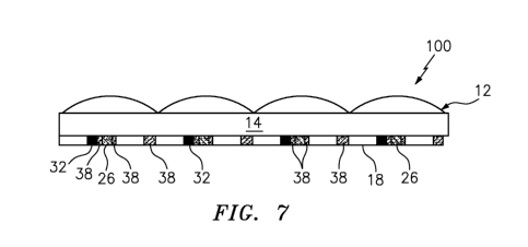
[0045] The optical device prepared in accordance with this method is shown
in
FIG. 7 and marked with reference number 100. There are three different cured
pigment
materials 26, 32, 38 (cured third pigmented material) in this case, two of
which (26, 32)
were directionally cured.
[0046] Referring now to FIG. 8, an observer, who is viewing the
device 100 from
the first cure angle, sees the synthetic image(s) associated with the cured
first
pigmented material 26. In FIGS. 8-10, the observer is "very far away" from the
device
such that the observer's effective angle to each of the focusing elements in
FIG. 8, for
example, is equivalent to the first cure angle. The synthetic image(s)
associated with the
cured first pigmented material 26 is only visible from the first cure angle.
[0047] An observer, who is viewing the device from the second cure angle
(see
FIG. 9), sees the synthetic image(s) associated with the cured second
pigmented
material 32. This synthetic image(s) is only visible from the second cure
angle.
[0048] An observer, who views the device from an angle which is not
one of the
cure angles (see FIG. 10), sees the synthetic image(s) associated with the
cured third
pigmented material 38. This synthetic image(s) is visible from any angle that
is not
equivalent to the first cure angle or the second cure angle. In some cases,
especially
those in which the optical device or system has a large f-number, an observer
may view
the device from a high angle (i.e., an angle far from the "normal" angle). As
the viewing
angle becomes high enough, the line of sight through a focusing element will
begin to
see the image icons that are underneath an adjacent focusing element. In this
type of
situation, an observer may see one or more synthetic images associated with a
specific
cure angle at an angle other than the specific cure angle.
[0049] The optical spacer or spacer layer may be formed using one or
more
essentially transparent or translucent polymers including, but not limited to,
12
CA 02943987 2016-09-26
WO 2015/148878 PCT/US2015/022907
polycarbonate, polyester, polyethylene, polyethylene napthalate, polyethylene
terephthalate, polypropylene, polyvinylidene chloride, and the like. In an
exemplary
embodiment, the optical spacer or spacer layer is formed using polyester or
polyethylene
terephthalate.
[0050] It is noted that while the use of an optical spacer or spacer layer
is
mentioned in the above exemplary embodiment, the optical device of the present
invention may also be prepared without an optical spacer or spacer layer.
[0051] Suitable radiation curable resins include, but are not limited
to, acrylics,
epoxies, polyesters, acrylated polyesters, polypropylenes, urethanes,
acrylated
urethanes, and the like. Preferably, the arrays are formed using an acrylated
urethane,
which is available from Lord Chemicals.
[0052] As previously mentioned, image icons formed from two or more
pigmented materials may be prepared by curing each material with collimated
light, or by
curing one material with collimated light and another material with another
means for
curing (e.g., radiation curing, chemical reaction). Synthetic images of the
image icons
formed from such directionally cured pigmented material(s) would be viewable
at the
cure angle(s), while synthetic images of the image icons formed from the non-
directionally cured pigmented materials would be viewable over a wide range of
angles.
It is noted that the arrangement(s) of image icons used in the practice of the
present
invention may also include prior art image icons formed in their entirety from
non-
directionally cured pigmented materials.
[0053] In one such exemplary embodiment, each image icon in the
arrangement(s) of image icons is formed from two cured pigmented materials,
each
having a different color. Here, each pigmented material is cured using
collimated light at
an angle through the focusing elements that is different from the angle used
to cure the
other pigmented material. In particular, this exemplary embodiment may be
produced by
curing a colored pigmented material using collimated light from one angle,
washing the
uncured pigmented material from the device, and then adding a second colored
pigmented material and curing it at a different angle. The resulting optical
device will
project a synthetic image(s) of a first color that is viewable at the first
cure angle, and a
synthetic image(s) of a second color that is viewable at the second cure
angle. As will
be readily appreciated, a large number of different color pigmented materials
could be
added this way. Additionally, another different color pigmented material is
added that is
13
CA 02943987 2016-09-26
WO 2015/148878 PCT/US2015/022907
cured without using collimated light, to provide a "background color" that can
be seen
from any angle that has not already been used for angular curing.
[0054] In another such exemplary embodiment, each image icon in the
arrangement(s) of image icons is formed from one cured fluorescent pigmented
material
and from one cured non-fluorescent pigmented material. Here, the fluorescent
feature,
which is detectable only at a given angle but not at another given angle, may
serve as
an effective machine readable authenticating feature.
[0055] In a further exemplary embodiment of the present invention,
the optical
device is a laser markable optical device that basically comprises the optical
device
described above, and optionally one or more layers located above and/or below
the
optical device, wherein at least one arrangement or layer of the optical
device or at least
one layer above or below the optical device is a laser markable arrangement or
layer.
[0056] The term "laser markable" or any variant thereof, as used
herein, is
intended to mean capable of physical or chemical modification induced or
formed by a
laser including, but not limited to, carbonizing, engraving, engraving with or
without color
change, engraving with surface carbonization, color change or internal
blackening, laser
marking by coating removal, ablation, bleaching, melting, swelling, and
vaporization, and
the like.
[0057] In a preferred embodiment, the inventive laser markable
optical device
has:
(a) an arrangement of optionally embedded focusing elements (e.g.,
embedded refractive focusing elements) and an arrangement of image icons that
are
separated by a laser markable layer that also functions as an optical spacer;
and/or
(b) one or more laser markable layers located below the optical device.
[0058] In the above preferred embodiment, which may be used in embedded
lens and other ID products (e.g., a patch embedded in a polymer ID card),
personalized
data in the form of static two dimensional (2D) images would be laser engraved
into or
below the optical device at an angle that differs from the angle(s) at which
the collimated
curing energy was applied.
[0059] In the latter embodiment where one or more laser markable layers are
located below the optical device, the arrangement of image icons contains
"vacant" icon
spaces. As previously mentioned, the "vacant" icon spaces are prepared using
unpigmented material(s) designed to not absorb laser light (e.g., UV curable
mixtures).
The unpigmented material(s) in this embodiment is directionally cured at the
same angle
14
CA 02943987 2016-09-26
WO 2015/148878 PCT/US2015/022907
that a laser engraver would use to write the static 2D images. The remainder
of the icon
recesses or voids in the arrangement of image icons are filled with pigmented
materials
cured at angles other than the angle used to cure the unpigmented material(s).
[0060] By way of this embodiment, laser energy is allowed to pass
through the
optical device with little laser energy being absorbed thereby, which provides
for superior
laser engraving through the optical device.
[0061] The present inventors have discovered that certain pigmented
materials
will absorb laser energy when an attempt is made to laser engrave through the
optical
device. The result is a defective laser-marked dark image with white or
missing areas.
This problem can be avoided by carefully choosing which pigments to use, or by
employing the above-mentioned "vacant" icon spaces. As will be readily
appreciated by
those skilled in the art, the use of "vacant" icon spaces allows for the use
of any pigment
without the concomitant risk of forming defective laser-marked dark images.
[0062] The net effect of the above-referenced embodiment is that the
colored,
pigmented synthetic image(s) would not be visible at the same angle that the
static 2D
laser engraved image(s) is visible. This means that there would be no pigment
in the
areas whether the focusing elements tend to focus the laser from the laser
engraver,
and the risk that the pigmented material(s) would absorb the laser energy is
avoided.
[0063] As alluded to above, to mark the laser markable optical device
of the
present invention, light energy from an engraving laser would be focused by
the focusing
elements and would engrave a laser markable layer in such a way that an image
would
be formed in the laser markable layer that is only viewable from the engraving
angle.
This technique allows for greater customization of the inventive device with a
dynamic,
personalized image that can be made to appear and disappear. Multiple laser
marking
angles can be used in the same device thereby providing multiple images, each
of which
is observable from a different viewing angle. In this way, short animations or
changing
images can be made in a personalized way. By way of example, when such a
device is
used on or in conjunction with an ID document, a small version of the portrait
used for
the ID document could be made to turn on and off. This dynamic portrait
displayed by
the inventive device would be unique to the ID document and would increase the
security of the document.
[0064] The resulting laser marked optical device would have one or
more laser
marked static 2D images on the laser markable layer(s). Here, the term "laser
marked"
CA 02943987 2016-09-26
WO 2015/148878 PCT/US2015/022907
or any variant thereof is intended to mean carrying or displaying any mark
formed by a
laser or laser-like device.
[0065]
Suitable laser markable layers may be prepared using thermoplastic
polymers. In
a first category, thermoplastic polymers with good absorption and
carbonization may be used. These polymers are laser markable in the absence of
so-
called laser additives, which are compounds absorbing light at the wavelength
of the
laser used, and converting it to heat. Examples of these polymers, which
produce
extensive blackening in the area exposed to the laser, include
polyethersulfone (PES),
polysulfone (PSU), polycarbonate (PC), and polyphenylene sulfide (PPS). In a
second
category, thermoplastic polymers with laser additives (e.g., pigments or
special
additives) may be used. Examples of these polymers, which can be marked
uniformly
and with good quality, include polystyrene (PS), styrene acrylonitrile (SAN),
acrylonitrile
butadiene styrene (ABS), PET, PETG, polybutylene terephthalate (PBT) and
polyethylene. Examples of these laser additives include carbon black, antimony
metal,
antimony oxide, tin-antimony mixed oxides, phosphorous-containing mixed oxides
of
iron, copper, tin and/or antimony, mica (sheet silicate) coated with metal
oxides. The
laser markable layers have preferred thicknesses ranging from about 5 to about
500
microns, more preferably from about 25 to about 200 microns.
[0066] In
a preferred laser marking technique, a V-Lase 10 Watt Q-switched
1064 nanometer (nm) laser marking system is used to mark the inventive laser
markable
device, the laser marking system producing laser light emission at a setting
of 30,000
Hertz (Hz). The laser marking system is set to 80% of maximum power, and a
scan
speed of 200 millimeters per second (mm/sec). These settings produce a high
contrast
mark in the desired location within the inventive laser markable device
without burning or
overexposure.
[0067] As
alluded to above, the present invention also provides sheet materials
and base platforms that are made from or employ the inventive optical device,
as well as
documents made from these materials.
The inventive optical device is also
contemplated for use with consumer goods as well as bags or packaging used
with
consumer goods.
[0068] By
way of example, the inventive optical device can be utilized in a variety
of different forms (e.g., strips, patches, security threads, planchettes) with
any banknote,
secure document or product for authentication purposes. For banknotes and
secure
documents, these materials are typically used in the form of a strip, patch,
or thread and
16
CA 02943987 2016-09-26
WO 2015/148878 PCT/US2015/022907
can be partially embedded within the banknote or document, or applied to a
surface
thereof. For passports or other ID documents, these materials could be used as
a full
laminate or inlayed in a surface thereof. For product packaging, these
materials are
typically used in the form of a label, seal, or tape and are applied to a
surface thereof.
As noted above, in one exemplary embodiment, the optical device is in the form
of a
patch embedded in a polymer ID card.
[0069] While various embodiments of the present invention have been
described
above, it should be understood that they have been presented by way of example
only,
and not limitation. Thus, the breadth and scope of the present invention
should not be
limited by any of the exemplary embodiments.
[0070] What is claimed is:
17