Note: Descriptions are shown in the official language in which they were submitted.
CA 02948284 2016-11-07
WO 2015/172189
PCT/AU2015/050186
1
IN LINE MANUFACTURING OF DOCUMENTS WITH SECURITY ELEMENTS
FIELD OF THE INVENTION
[0001] The invention relates to documents with security elements used as an
anti-counterfeiting measure. In particular the invention relates to documents
with
integral security elements and a method and apparatus for the 'in line'
manufacture of these security documents.
BACKGROUND OF THE INVENTION
[0002] The use of security elements is well established in the field of
security
documents. One such type of security element is an optically variable device
(OVD) which is a security feature or device that changes in appearance. OVDs
provide an optically variable effect when the banknote is tilted and/or when
the
viewing angle of the observer relative to the OVD changes. The image of an OVD
may also be changed by aligning a verification device over the security
feature or
device. An OVD may be provided by a printed area, e.g. an area printed with
metallic inks or iridescent inks, by an embossed area, and by a combination of
a
printed and embossed feature. An OVD may also be provided by a diffractive
device, such as a diffraction grating or a volume hologram and may include
arrays of microlenses and lenticular lenses.
[0003] Lens-based security devices are a type of optically variable device
(OVD). A description of cylindrical microlenses arranged in a lenticular array
to
make an OVD is provided in 'Optical Document Security', 3rd Edition by Rudolf
L.
Van Renesse ISBN 1-58053-258-6, pages 162 and 163, published 2005. The
lenticular array is a series of cylindrical microlenses moulded in a polymer
substrate. The microlens array can be placed on printed images and indicia
such
that when viewed from different angles, different images of the underlying
indicia
are seen. This technology can also be used with spherical or part-spherical
microlenses and micro-images to produce magnified images by moire
CA 02948284 2016-11-07
WO 2015/172189
PCT/AU2015/050186
2
magnification, and to give an illusion of depth or movement as the underlying
image is viewed from various angles.
[0004] Security elements, such as microlens arrays and other types of OVDs,
such as diffraction gratings and volume holograms, are usually made separately
from the remainder of the security document and subsequently applied to the
document substrate to complete the security document. For example the OVDs
are formed as a repeating pattern in a polymer substrate and wound into a
roll.
Then, in a completely separate process, the OVDs are applied to a designated
area on the remainder of the security document.
[0005] Unfortunately, microlens structures and other types of security
elements which have a structured surface, such as volume holograms,
necessarily have a height or profile that gives the security document a
significant
localised increase in thickness. Typically the thickness can increase by about
30% or more in the area occupied by the security device. This localised
thickness increase compounds when the security documents are stacked on top
of each other. Similarly, if the security element is applied to a continuous
web of
the security documents and subsequently wound into a roll, the roll quickly
develops a large eccentricity which generates downstream problems in the
production process. The distortion in the roll causes some slack areas in the
web
and areas of excessive tension in the web where the web may burst or shows
signs of "pressure blocking". Pressure blocking occurs where two surfaces are
brought into close contact with each other under pressure and, as a result of
pressure surface entanglement or Van der Waal forces, the level of adhesion
between the surfaces increases to such an extent that a significant force is
required to part them. On occasion the force can exceed the cohesive strength
of
the two surfaces resulting in rupturing one or more of the surfaces.
[0006] If the security documents are a stack of separate sheets, the
thickness
variation in the stack creates complications when the sheets are fed or
delivered
through a sheet transport system. If the security document is a bank note,
then a
CA 02948284 2016-11-07
WO 2015/172189
PCT/AU2015/050186
3
stack of the notes in a cash issuing and processing machine will form a wedge
shape which limits the number of notes that can be processed at any one time.
Portions of the stack can be regularly rotated 1800 in order to produce a
stack
that is flatter. However, if the OVD is around the middle of the note, turning
sections of the stack tends to be less effective at flattening the stack.
[0007] Wedge-
shaped stacks limit the number of notes that can be processed
at one time and increase processing costs. Rotating the notes within a stack
introduces complexity and complications with note authentication. Furthermore,
the production of the OVDs separately from the remainder of the document
substantially increases the production costs relative to a security document
compared with a type of security device that can be formed in a single 'in
line'
manufacturing process.
SUMMARY OF THE INVENTION
[0008]
According to a first aspect, the present invention provides a method of
manufacturing a security document with a structured security element, wherein
the method comprises:
(a) providing a document substrate having a first surface on one side and
an
second surface on the opposite side;
(b) applying a radiation sensitive coating to a security element area on
the first
surface of the document substrate;
(c) forming the security element in the radiation coating, the security
element
having a structure extending to a height from the first surface;
(d) applying one or more additional layers to the first surface of the
substrate,
excluding the security element area;
CA 02948284 2016-11-07
WO 2015/172189 PCT/AU2015/050186
4
(e) wherein the one or more additional layers have a combined thickness
which differs from the height of the security element structure by less than
50% of the height of the security element structure and/or by less than 10
pm.
[0009] The combined thickness of the additional layer or layers is
preferably
substantially equal to the height of the security element structure. Where the
combined thickness of the additional layer or layers differs from the height
of the
security element structure, the difference is preferably less than 20%, more
preferably less than 15%, and even more preferably less than 10% of the height
of the security element structure. In a particularly preferred embodiment, the
predetermined amount is less than 5 pm.
[0010] Preferably, the method of manufacturing the security document
further
includes: providing the document substrate as a continuous web; and feeding
the
web through a series of processing stations in a machine direction for
application
of the radiation sensitive coating, for forming the security element in the
radiation
sensitive coating, and for the application of the one or more additional
layers such
that the continuous web with the security element and the additional layers is
collected downstream of the processing stations in a substantially cylindrical
roll.
[0011] According to a second aspect, the present invention provides
apparatus for manufacturing a security document with a structured security
element comprising a series of processing stations including: a substrate
feeding
station for feeding a continuous web of document substrate having a first
surface
on one side and a second surface on its opposite side; a station for applying
a
radiation sensitive coating to a security element area on the first surface of
the
document substrate; a security element forming station for forming a
structured
security element in the radiation sensitive coating, the security element
comprising a structure extending to a height from the first surface; and a
station
for applying one or more additional layers to the first surface of the
substrate,
excluding the security element area, wherein the one or more additional layers
CA 02948284 2016-11-07
WO 2015/172189
PCT/AU2015/050186
have a combined thickness which differs from the height of the security
element
structure by less than 50% of the height of the security element structure
and/or
by less than 10 pm.
[0012] One or more of the processing stations in the method or apparatus
may include a roller assembly. The radiation sensitive coating is preferably
applied by a coating applying roller only in the security element area. The
station
for applying the one or more additional layers may also include one or more
rollers for applying one or more additional layers in the form of at least one
opacifying layer to the first surface in a printing or laminating process.
[0013] The radiation sensitive coating is preferably applied by a printing
process, such as flexographic printing; gravure printing; or silkscreen
printing.
[0014] The radiation sensitive coating may be an embossable, radiation-
curable coating which can be embossed to form a security element having a
relief
structure, such as a diffractive structure or a lens structure. In this case,
an
embossing station for embossing the security element structure and a curing
station for curing the radiation-curable coating are provided. The curing
station for
curing the radiation-curable coating is preferably provided at the embossing
station, so that the embossed structure of the security element is cured at
substantially the same time as the curable coating is embossed.
[0015] Preferably the radiation-curable coating is a UV-curable coating,
such
as a UV-curable, epoxy based coating.
[0016] Alternatively, other forms of embossable curable coatings and curing
systems may be used, such as electron-beam (EB) curable coatings, or cationic
curing coatings.
[0017] Preferably the curable coating is embossed via contact with a
security
element applying roller. Preferably the curable coating is liquid prior to
contact
CA 02948284 2016-11-07
WO 2015/172189 PCT/AU2015/050186
6
with the security element applying roller. In the case of a UV-curable
coating, the
embossed coating is exposed to UV radiation incident on the second surface
which may be transmitted through the translucent or transparent polymer layer.
[0018] Preferably the security element roller has a cylindrical embossing
surface completely covered with a repeating security element structure
pattern.
Optionally the cylindrical embossing surface is engraved with discrete
formations
shaped to correspond with the shape of the discrete security element on the
security document. Preferably a cylindrical embossing surface of the security
element applying roller is engraved using a diamond stylus of suitable cross-
section. Optionally the cylindrical embossing surface of the security element
applying roller is provided by a metal shim wrapped around a support surface
on
the roller.
[0019] Alternatively, or additionally, the radiation sensitive coating may
be a
photo-sensitive coating which can be irradiated with radiation of a suitable
range
of wavelengths to form a security element, such as a volume hologram, a
polarising security device or a liquid crystal security device. In this case,
a
radiation source for irradiating the radiation sensitive coating is provided.
[0020] The first surface of the document substrate may be subjected to an
adhesion promoting process prior to application of the radiation sensitive
coating.
Optionally, the adhesion promoting process is selected from: flame treatment;
corona discharge treatment; and plasma treatment.
[0021] The method may further include applying an adhesion promoting layer
or a primer layer to the first surface of the document substrate prior to
applying
the radiation sensitive coating. Preferably the adhesion promoting layer
raises
the surface energy of the first surface by at least five dynes more than the
surface
energy of the adhesion promoting layer. In a further preferred form, the
surface
energy of the first surface is raised at least ten dynes more than that of the
adhesion promoting layer. The adhesion promoting layer may comprise one or
CA 02948284 2016-11-07
WO 2015/172189
PCT/AU2015/050186
7
more of: a UV-curing layer; a solvent based layer; and a water based layer.
Preferably, the adhesion promoting layer is dried before the radiation
sensitive
coating is applied.
[0022] In one embodiment, the security element structure comprises at least
one focussing element. The at least one focussing element may be an array of
microlenses, although other forms of focussing elements, such as diffractive
lenses, Fresnel lenses and zone plates may be provided to form the security
element structure.
[0023] The at least one focussing element may be an array of cylindrical or
part cylindrical lenses. The cylindrical or part-cylindrical lenses may extend
substantially parallel to one another or in a plurality of different
directions.
Alternatively, the at least one focussing element may be a microlens array in
which the lens structures are spherical, part-spherical or aspherical
microlenses.
Optionally, the security element structure may be a microlens array in which
the
lens structures are a combination of cylindrical or part-cylindrical
microlenses and
spherical, part-spherical or aspherical microlenses.
[0024] In another embodiment, the security element comprises a diffractive
structure, such as a diffraction grating, or a hologram. A diffraction grating
may be
formed by embossing a radiation-curable coating in similar manner to forming
an
embossed lens structure.
[0025] In a further embodiment, the security element structure may be
formed
by irradiating the radiation sensitive coating with patterned radiation. In
this
embodiment, the radiation sensitive coating may be a photopolymer.
[0026] A volume hologram may be formed by applying the radiation sensitive
coating using a printing and/or embossing process, and irradiating the
radiation
sensitive material with patterned radiation configured for recording the
volume
hologram within the radiation sensitive coating. Our Australian Provisional
CA 02948284 2016-11-07
WO 2015/172189 PCT/AU2015/050186
8
Application No. 2014901478 entitled Volume Holograms for Security Documents
filed on 24 April 2014 describes one such method for producing a volume
hologram in a structured security document. The radiation sensitive material
is
preferably a printable photopolyrner.
[0027] In a further embodiment, the security element comprises a polarising
device. A polarising device may be formed by applying a radiation sensitive
coating which is irradiated with patterned radiation for applying the
polarising
device within the radiation sensitive coating. In this embodiment, the
radiation
sensitive coating may be a photopolymer, or a photosensitive liquid crystal
layer.
[0028] A protective coating may be applied to the security element
structure at
a further processing station downstream of the station for forming the
security
element structure in the radiation sensitive layer. A protective coating is
particularly required when the security element is a diffractive structure or
a
hologram. The protective coating is preferably substantially transparent so
that it
does not affect the optical properties of the security element.
[0029] Optionally, one or more second surface coatings are applied to the
second surface. Optionally, the additional coatings are translucent or
transparent. Optionally, the additional coatings include at least one layer
that is
pigmented and applied as indicia to be viewed on the security document.
Optionally the one or more additional coatings include a layer that is
contiguous
across the first surface except for the security element area.
[0030] In one preferred embodiment, a printed layer is applied to the
second
surface of the document substrate in an area corresponding to the security
element area on the first surface, wherein the printed layer has indicia
forming
part of an image to be viewed through the security element.
[0031] According to another aspect of the invention there is provided a
security document made by the method of the first aspect of the invention.
CA 02948284 2016-11-07
WO 2015/172189
PCT/AU2015/050186
9
[0032] According to a further aspect of the invention, there is provided a
security document comprising: a document substrate having a first surface on
one side and a second surface on the opposite side; a security element
positioned on a security element area of the first surface, the security
element
having a structure that extends to a height from the first surface; and one or
more
additional layers on the first surface of the document substrate, but
excluding the
security element area; wherein the one or more additional layers have a
combined thickness which differs from the height of the security element
structure
by less than 50% of the height of the security element structure and/or by
less
than 10 p.m.
[0033] The combined thickness of the additional layer or layers is
preferably
substantially equal to the height of the security element structure. Where the
combined thickness of the additional layer or layers differs from the height
of the
security element structure, the difference is preferably less than 20%, more
preferably less than 15%, and even more preferably less than 10% of the height
of the security element structure. In a particularly preferred embodiment, the
difference is less than 5 pm.
[0034] In one embodiment, the security element structure comprises at least
one focussing element. The at least one focussing element may be an array of
microlenses, although other forms of focussing elements, such as diffractive
lenses, Fresnel lenses and zone plates may be provided to form the security
element structure.
[0035] The at least one focussing element may be an array of cylindrical or
part cylindrical lenses. The cylindrical or part-cylindrical lenses may extend
substantially parallel to one another or in a plurality of different
directions.
Alternatively, the at least one focussing element may be a microlens array in
which the lens structures are spherical, part-spherical or aspherical
microlenses.
Optionally, the security element structure may be a microlens array in which
the
CA 02948284 2016-11-07
WO 2015/172189 PCT/AU2015/050186
lens structures are a combination of cylindrical or part-cylindrical
microlenses and
spherical, part-spherical or aspherical microlenses.
[0036] In another embodiment, the security element comprises a diffractive
structure, such as a diffraction grating, a hologram or a volume hologram.
[0037] In a further embodiment, the security element comprises a polarising
device and/or a liquid crystal device.
[0038] Preferably, the document substrate is formed from a transparent or
translucent polymeric material, such as biaxially oriented polypropylene. The
additional layer or layers applied to the first surface of the substrate are
preferably
opacifying layers which are omitted in the security element area to form a
window
of half window area that contains the security element. The opacifying layers
are
preferably opacifying coatings of ink which may be applied in a printing
process.
Alternatively, the additional layer or layers may be layers of a substantially
opaque material, such as paper or opaque plastics material that is laminated
or
otherwise secured to the substrate.
[0039] In one embodiment, the security element area is in the form of a
stripe
across the security document. Optionally the security element area is a
discrete
region of the security document. Optionally the discrete region is in the form
of a
graphical design.
[0040] Preferably the security document further comprises a printed layer
applied to the second surface in an area corresponding to the security element
area on the first surface wherein the printed layer has indicia forming part
of an
image to be viewed through the security element. Where the security element is
an array of focussing elements, the printed indicia may comprise an array of
corresponding microimages.
[0041] Preferably, the security document is a banknote.
CA 02948284 2016-11-07
WO 2015/172189
PCT/AU2015/050186
11
[0042] Skilled workers in this field will readily appreciate that the
invention
allows for the production of security documents with security element
structures,
such as optically variable devices (OVDs), via an in line manufacturing
process
rather than the separate or parallel processes discussed in the background
section. When printing security documents such as banknotes, the production
volumes are very high and strongly favour printing onto a continuous web
between a feed roller and a collection roller. By producing the entire
security
document including the security element structure in accordance with the
present
invention allows for in line manufacturing by eliminating the non-cylindrical
roll
forming on the collection roller. In light of this, the single in line
manufacturing
process provides significant time and cost efficiencies in the production of
the
security documents. Furthermore, the present invention provides for in line
manufacturing of a security element structure in a shape which is not merely a
simple stripe or basic geometric patch, but potentially a more exotic and
intricate
shape.
[0043] The in line manufacturing technique of the present invention allows
for
the layers around the security element structure to be built up, thereby
substantially reducing or eliminating any localised increases in the document
thickness. It will be appreciated that localised decreases in thickness, such
as
within a window or half window opening in the second surface layers, do not
cause the problems associated with localised thickness increases.
[0044] The in line process of the invention also allows the security
element
structure to be positioned in accurate registration with other features of the
security document. This further raises the technological challenges faced by
would-be counterfeiters.
Security Document or Token
[0045] As used herein the term security documents and tokens includes all
types of documents and tokens of value and identification documents including,
but not limited to the following: items of currency such as banknotes and
coins,
CA 02948284 2016-11-07
WO 2015/172189 PCT/AU2015/050186
12
credit cards, cheques, passports, identity cards, securities and share
certificates,
driver's licenses, deeds of title, travel documents such as airline and train
tickets,
entrance cards and tickets, birth, death and marriage certificates, and
academic
transcripts.
[0046] The invention is particularly, but not exclusively, applicable to
security
documents or tokens such as banknotes or identification documents such as
identity cards or passports formed from a substrate to which one or more
layers
of printing are applied.
Security Element
[0047] As used herein the term security device or feature includes any one
of
a large number of security devices, elements or features intended to protect
the
security document or token from counterfeiting, copying, alteration or
tampering.
Security devices or features may be provided in or on the substrate of the
security
document or in or on one or more layers applied to the base substrate, and may
take a wide variety of forms, such as security threads embedded in layers of
the
security document; security inks such as fluorescent, luminescent and
phosphorescent inks, metallic inks, iridescent inks, photochromic,
thermochromic,
hydrochromic or piezochromic inks; printed and embossed features, including
relief structures; interference layers; liquid crystal devices; lenses and
lenticular
structures; optically variable devices (OVDs) such as diffractive devices
including
diffraction gratings, holograms, volume holograms and diffractive optical
elements
(DOEs).
Substrate
[0048] As used herein, the term substrate refers to the base material from
which the security document or token is formed. The base material may be paper
or other fibrous material such as cellulose; a plastic or polymeric material
including but not limited to polypropylene (PP), polyethylene (PE),
polycarbonate
(PC), polyvinyl chloride (PVC), polyethylene terephthalate (PET), biaxially-
oriented polypropylene (BOPP); or a composite material of two or more
materials,
CA 02948284 2016-11-07
WO 2015/172189
PCT/AU2015/050186
13
such as a laminate of paper and at least one plastic material, or of two or
more
polymeric materials.
Transparent Windows and Half Windows
[0049] As used herein the term window refers to a transparent or
translucent
area in the security document compared to the substantially opaque region to
which printing is applied. The window may be fully transparent so that it
allows
the transmission of light substantially unaffected, or it may be partly
transparent
or translucent partially allowing the transmission of light but without
allowing
objects to be seen clearly through the window area.
[0050] A window area may be formed in a polymeric security document which
has at least one layer of transparent polymeric material and one or more
opacifying layers applied to at least one side of a transparent polymeric
substrate,
by omitting least one opacifying layer in the region forming the window area.
If
opacifying layers are applied to both sides of a transparent substrate a fully
transparent window may be formed by omitting the opacifying layers on both
sides of the transparent substrate in the window area.
[0051] A partly transparent or translucent area, hereinafter referred to as
a
"half-window", may be formed in a polymeric security document which has
opacifying layers on both sides by omitting the opacifying layers on one side
only
of the security document in the window area so that the "half-window" is not
fully
transparent, but allows some light to pass through without allowing objects to
be
viewed clearly through the half-window.
[0052] Alternatively, it is possible for the substrates to be formed from a
substantially opaque material, such as paper or fibrous material, with an
insert of
transparent plastics material inserted into a cut-out, or recess in the paper
or
fibrous substrate to form a transparent window or a translucent half-window
area.
CA 02948284 2016-11-07
WO 2015/172189
PCT/AU2015/050186
14
Embossable Curable Ink
[0053] The term embossable curable ink used herein refers to any ink,
lacquer or other coating which may be applied to the substrate in a printing
process, and which can be embossed while soft to form a relief structure and
cured to fix the embossed relief structure. The curing process does not take
place
before the curable ink is embossed, but it is possible for the curing process
to
take place either after embossing or at substantially the same time as the
embossing step. The curable ink is preferably a radiation curable ink curable
by
radiation, such as ultraviolet (UV) radiation. Alternatively, the radiation
curable ink
may be cured by other forms of radiation, such as electron beams or X-rays.
[0054] The radiation curable ink is preferably a transparent or translucent
ink
formed from a clear resin material. Such a transparent or translucent ink is
particularly suitable for printing light-transmissive security elements such
as sub-
wavelength gratings, transmissive diffractive gratings and lens structures.
[0055] In one particularly preferred embodiment, the transparent or
translucent ink preferably comprises an acrylic based UV curable clear
embossable lacquer or coating.
[0056] Such UV curable lacquers can be obtained from various
manufacturers, including Kingfisher Ink Limited, product ultraviolet type UVF-
203
or similar. Alternatively, curable embossable coatings may be based on other
curing systems, such as EB curing systems or cationic curing systems.
[0057] The radiation curable inks and lacquers used herein have been found
to be particularly suitable for embossing microstructures, including
diffractive
structures such as diffraction gratings and holograms, and rnicrolenses and
lens
arrays. However, they may also be embossed with larger relief structures, such
as non-diffractive optically variable devices.
CA 02948284 2016-11-07
WO 2015/172189
PCT/AU2015/050186
[0058] The ink is preferably embossed and cured by ultraviolet (UV)
radiation
at substantially the same time. In a particularly preferred embodiment, the
radiation curable ink is applied and embossed at substantially the same time
in a
Gravure printing process.
[0059] Preferably, in order to be suitable for Gravure printing, the
radiation
sensitive coating has a viscosity falling substantially in the range from
about 20 to
about 175 centipoise, and more preferably from about 30 to about 150
centipoise.
The viscosity may be determined by measuring the time to drain the lacquer
from
a Zahn Cup #2. A sample which drains in 20 seconds has a viscosity of 30
centipoise, and a sample which drains in 63 seconds has a viscosity of 150
centipoise.
[0060] With some polymeric substrates, it may be necessary to apply an
intermediate layer to the substrate before the radiation sensitive coating is
applied
to improve the adhesion of the embossed structure formed by the ink to the
substrate. The intermediate layer preferably comprises a primer layer, and
more
preferably the primer layer includes a polyethylene imine. The primer layer
may
also include a cross-linker, for example a multi-functional isocyanate.
Examples
of other primers suitable for use in the invention include: hydroxyl
terminated
polymers; hydroxyl terminated polyester based co-polymers; cross-linked or
uncross-linked hydroxylated acrylates; polyurethanes; and UV curing anionic or
cationic acrylates. Examples of suitable cross-linkers include: isocyanates;
polyaziridines; zirconium complexes; aluminium acetylacetone; melamines; and
carbodi-imides.
BRIEF DESCRIPTION OF THE DRAWINGS
[00611 The invention will now be described by way of example only with
reference to the accompanying drawings, in which:
CA 02948284 2016-11-07
WO 2015/172189 PCT/AU2015/050186
16
Figure 1 is a schematic representation of apparatus for in line
manufacturing of a security document with a security element structure;
Figure 2 is a schematic cross-section of a security document with a
security element structure in the form of a lens-based security device;
Figure 3 is a schematic cross-section of a security document with a
security element structure in the form of a volume hologram; and
Figure 4 is a schematic cross section of a modified security document with
a security element structure in the form of a volume hologram.
DETAILED DESCRIPTION OF THE PREFERRED EMBODIMENTS
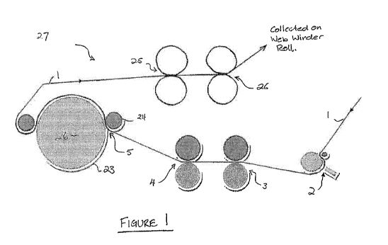
[0062] Referring to Figure 1, apparatus 27 for in line manufacture of the
security documents is schematically shown. A continuous web of translucent or
transparent material such as polypropylene, PET or the like is subject to an
adhesion promoting process at a first processing station 2 including a roller
assembly. Suitable adhesion promoting processes are flame treatment, corona
discharge treatment, plasma treatment or similar. The adhesion promoting
process raises the surface energy of the security document substrate 1 such
that
the energy of a first surface 11 (see Fig. 2) is more than 5 and preferably
more
than 10 dynes greater than that of an adhesion promoting layer that is next
applied to the first surface 11 of the document substrate 1.
[0063] An adhesion promoting layer 28 is applied at a second processing
station 3 including a roller assembly. A suitable adhesion promoting layer is
one
specifically adapted for the promotion of adhesion of UV curable coatings to
polymeric surfaces. The adhesion promoting layer may have a UV curing layer, a
solvent-based layer, a water-based layer or any combination of these.
Preferably, the adhesion promoting layer has a primer layer that typically
includes
a polyethylene ionine. The primer layer may also include a cross linker, for
CA 02948284 2016-11-07
WO 2015/172189
PCT/AU2015/050186
17
example a multifunctional isocyanate. Examples of suitable primers for use
with
the present invention include: hydroxyl terminated polymers; hydroxyl
terminated
polyester based co-polymers; cross-lined or uncross-linked hydroxylated
acrylates; polyurethanes; and UV curing anionic or cationic acrylates.
Examples
of suitable cross-linkers include: isocyanates; polyaziridines; zirconium
complexes; aluminium acetylacetone; melamines; and carbodi-imides.
[0064] The type of primer is selected to best suit the radiation sensitive
coating for forming the security element. The selected primer should not
substantially affect the optical properties of the security element 17; 37
(Figs.2
and 3) that is eventually formed.
[0065] At a third processing station 4, which also includes a roller
assembly,
the radiation sensitive coating, is applied to the dried surface of the
adhesion
promoting layer 28. The radiation sensitive coating can be applied via
flexographic printing, gravure printing or a silk screen printing process.
[0066] The radiation sensitive coating is only applied to the security
element
area 22 (see Figs. 2 and 3) on the first surface 11 where the OVD 16 is to be
positioned. The security element area 22 can take the form of a stripe, a
discrete
patch in the form of a simple geometric shape or in the form of a more complex
graphical design.
[0067] While the radiation sensitive coating is still liquid, it is
processed to
form the security element structures 17; 37 (shown in Figures 2 and 3) at a
fourth
processing station 5.
[0068] In one embodiment, processing station 5 includes an embossing roller
6. Embossing roller 6 has a cylindrical embossing surface 23 for embossing an
security element structure, such as a lens structure 17 (Fig. 2) into a
radiation
sensitive coating in the form of a UV curable ink. The cylindrical embossing
surface 23 has surface relief formations corresponding to the shape of the
CA 02948284 2016-11-07
WO 2015/172189 PCT/AU2015/050186
18
security element structure to be formed. In one embodiment, the surface relief
formations can orient microlenses 17 in the machine direction, transverse to
the
machine direction, or in multiple directions at any angle to the machine
direction.
The microlenses 17 may be cylindrical, part-cylindrical, spherical, part-
spherical,
aspherical or an alternative design, or indeed a combination of various types
of
microlens structures. Alternatively, the cylindrical embossing surface 23 of
the
embossing roller 6 may have surface relief formations for embossing a
diffractive
structure, or other embossed OVD structure, into the UV curable ink.
[0069] The cylindrical embossing surface 23 of the embossing roller 6 may
have a repeating pattern of surface relief formations or the relief structure
formations may be localised to individual shapes corresponding to the shape of
the security element area 22 on the document substrate 1. The embossing roller
6 may have the surface relief formations formed by a diamond stylus of
appropriate cross section, or the surface relief formations may be provided by
at
least one metal shim provided on the embossing roller 6. The at least one
metal
shim may be attached via adhesive tape, magnetic tape, clamps or other
appropriate mounting techniques.
[0070] The UV curable ink on the substrate is brought into intimate contact
with the cylindrical embossing surface 23 of the embossing roller 6 by a UV
roller
24 at processing station 5 such that the liquid UV curable ink flows into the
surface relief formations of the cylindrical embossing surface 23. At this
stage,
the UV curable ink is exposed to UV radiation transmitted though the substrate
layer 1. The UV radiation may be transmitted through the surface of the UV
roller
24. The UV roller 24 preferably has internal UV lamps and a roller surface
that is
UV transparent in at least some areas.
[0071] By careful selection of the UV curable materials and/or the
radiation
source it is possible to create the security element structure at a later
stage of the
in line manufacturing process. The radiation intensity must be sufficient to
penetrate all layers between the UV curable ink and the radiation source. For
CA 02948284 2016-11-07
WO 2015/172189
PCT/AU2015/050186
19
example, it is possible to use E-beam curing or metal doped microwave
discharge
lamps as the radiation source. Alternatively, the UV curable ink may include a
photo initiator that is tuned to absorb the emissions from an appropriate
light
source.
[0072] The UV cylinder 24 and the embossing cylinder 6 may use a
registration device to accurately register the radiation sensitive coating
with the
security element area 22 on the document substrate 1. A suitable method for
accurate registration of the embossing cylinder with the radiation sensitive
coating
in the designated security element area 22 on the substrate 1 is described in
greater detail in WO 2008/031170 to the present applicant.
[0073] With the security element structure 17 applied to the document
substrate 1, one or more additional layers are applied at a downstream
processing station including further roller assemblies 25 and 26. The
additional
layers may be clear or pigmented coatings and applied as a partial coating, as
a
contiguous coating or a combination of both. In one preferred method, the
additional layers are opacifying layers which are applied to one or both
surfaces
of the substrate 1 except in the region of the security element structure.
[0074] Figure 2 schematically shows a security document 10 formed with an
embossed security element structure 17 in the form of a lens structure having
an
array of microlenses manufactured in accordance with the method of the
invention. The security document comprises a transparent substrate of
polymeric
material, preferably biaxially oriented polypropylene (BOPP), having a first
surface 11 and a second surface 12. Opacifying layers 13, 14 and 15 are
applied
to the first surface having a combined total thickness T. The opacifying
layers are
omitted in a window area 16 where the security element structure 17 is applied
to
the first surface 11. The microlenses of the embossed security element
structure17 have a height H.
CA 02948284 2016-11-07
WO 2015/172189 PCT/AU2015/050186
[0075] In a preferred embodiment, the combined thickness T of the
opacifying
layers 13, 14 and 15 is preferably substantially equal to the height H of the
security element structure 17. Where there is any difference between the
height H
of the embossed security element structure 17 and the combined thickness T of
the opacifying layers 13, 14 and 15, the difference is less than 50%,
preferably
less than 20%, more preferably less than 15%, and even more preferably less
than 10% of the height of the security element structure. The difference is
preferably less than 10 gm. In a particularly preferred embodiment, the
difference
is less than 5 p,m..
[0076] As shown in Figure 2, opacifying layers 20, 21 applied to the second
surface 12 on the opposite side of the substrate 1 are omitted in a window
area
19. The window area 19 substantially coincides with the window area 16 on the
first surface. The window area 19 shown in Figure 2 is smaller than the window
area 16, though it will be appreciated that the relative sizes and locations
of the
window areas 16 and 19 may be changed. In one preferred embodiment, the
window areas are of the same size.
[0077] A printed layer 18 may be applied to the second surface 12 on the
opposite side of the substrate in the window area 19. The printed layer 19 may
form an image or images viewable through the security element structure 17.
When the embossed security element structure is an array of microlenses, the
printed area 19 may include a corresponding array of microimages.
[0078] In an alternative embodiment, the radiation sensitive coating may be
a
photosensitive polymer, with a radiation source provided at the processing
station
5 for irradiating the radiation sensitive coating with patterned radiation to
form an
security element structure 37 (see Fig. 3) in the radiation sensitive coating.
In this
case, the security element structure may comprise a volume hologram, a
polarising device or a liquid crystal device.
CA 02948284 2016-11-07
WO 2015/172189
PCT/AU2015/050186
21
[0079] Figure 3 shows a security document 30 comprising a transparent
polymeric substrate 1 with a security element structure 37, such as a volume
hologram, a polarising device or a liquid crystal device, formed in a
radiation
sensitive coating 31 applied to the first surface 11 of the substrate. An
optional
protective coating 35 is applied over the security element structure 37. The
security element structure 37, including the optional protective coating 31,
has a
height H, which may typically range from about 101.im to about 30 tim. At
least
one opacifying layer 32 is applied to the first surface '11 except in a window
area
36 where the radiation sensitive coating 31 forming the security element 37 is
applied to the first surface 11. Although only one opacifying layer 32 is
shown in
Figure 3, it will be appreciated that two or more opacifying layers may be
applied
to the first surface as described with reference to Figure 2. The at least one
opacifying layer 32 has a thickness T.
[0080] In a preferred embodiment, the thickness T of the opacifying
layer(s)
32 is preferably substantially equal to the height H of the security element
structure 37 including any protective coating 35. Where there is any
difference
between the height H of the security element structure 37 and the thickness T
of
the opacifying layer(s) 32, the difference is less than 50%, preferably less
than
20%, more preferably less than 15%, and even more preferably less than 10% of
the height of the security element structure. The difference is preferably
less than
urn. In a particularly preferred embodiment, the difference is less than
51.tm.
[0081] As shown in Figure 3, at least one opacifying layer 34 is applied to
the
second surface 12 on the opposite side of the substrate 1 to completely cover
the
second surface 12 so that the security element structure is provided in a half-
window.
[0082] Figure 4 shows a modified embodiment similar to that of Figure 3 and
corresponding reference numerals have been applied to corresponding parts. The
embodiment of Figure 4 differs from that of Figure 3 in that the at least one
opacifying layer 34 is omitted in a window area 39. The window area 39
CA 02948284 2016-11-07
WO 2015/172189
PCT/AU2015/050186
22
substantially coincides with the window area 36 on the first surface. The
window
area 39 shown in Figure 4 is the same size as the window area 16, though it
will
be appreciated that the relative sizes and locations of the window areas 16
and
19 may be changed.
[0083] Keeping any difference between the corn bined thickness T of the one
or more additional layers 13, 14, 15; 32 and the height H of the security
element
structure to less than 50%, preferably less than 20%, more preferably less
than
15%, and even more preferably less than 10%, of H, and less than 10 Rrn, more
preferably less than 5 lial, substantially reduces the localised thickness
increase
of the security element structure, and allows the continuous web of documents
10
to be wound onto a collection roller. Collecting the documents 10 in a
substantially cylindrical roll avoids the pressure blocking and other web
tension
problems normally associated with the in line manufacture of documents
authenticated with security element structures such as lens-based devices and
volume holgrams. Similarly, security documents according to the invention can
form a stack of separate sheets and maintain a substantially flat profile.
This
makes sheet feed systems less problematic and avoids the need to rotate equal
portions of the stack by 180 .
[0084] Workers in this field will appreciate that localised thickness
decreases,
or recesses, in the document do not present the same drawbacks as an area of
increased thickness or height. As shown in Figs.2 and 4, the corresponding
region 19; 39 opposite the security element structure 16 has a window area 39
formed by the opacifying layer(s) 20, 21; 34 being omitted in the region of
the
security element structure. This window area 39 is relatively small compared
to
the overall security document. Stacking documents with localised recesses will
not result in wedge-shaped stacks; merely small voids within the stack that
are
inconsequential in sheet feed systems or in line manufacturing processes. In
addition, security documents manufactured in accordance with the invention
also
allow for more efficient stacking of the finished security documents in cash
machines and cash processing machines with less need for manual intervention.
CA 02948284 2016-11-07
WO 2015/172189
PCT/AU2015/050186
23
[0085] A skilled addressee will readily recognise many variations and
modifications to the described embodiments, which do not depart from the
spirit
and scope of the broad inventive concept.