Note: Descriptions are shown in the official language in which they were submitted.
CA 02995538 2018-02-13
WO 2017/029327 PCT/EP2016/069517
1
VOLTAGE SOURCE CONVERTER AND CONTROL THEREOF
This application relates to a voltage source converter and to methods and
apparatus
for control of a voltage source converter, and especially to a voltage source
converter
for use in high voltage power distribution and in particular to a voltage
source converter
having elements for voltage wave-shaping that may be shared between arms of a
phase limb.
HVDC (high-voltage direct current) electrical power transmission uses direct
current for
the transmission of electrical power. This is an alternative to alternating
current
electrical power transmission which is more common. There are a number of
benefits
to using HVDC electrical power transmission.
In order to use HVDC electrical power transmission, it is typically necessary
to convert
alternating current (AC) to direct current (DC) and back again. Historically
this has
involved a six pulse bridge type topology based on elements such thyristors
which, can
be turned on at a desired point in the power cycle and remain conducting as
long as
they are forward biased. Such a converter is known as a line-commutated
converter
(LCC).
Recent developments in the power electronics field have led to an increased
use of
voltages-source converters (VSC) for AC-DC and DC-AC conversion. VSCs make use
of series connected switching elements, typically insulated gate bipolar
transistors
(IGBTs) connected with respective antiparallel diodes, that can be
controllably turned
on and off. Such converters are sometimes referred as self-commutated
converters.
VSCs typically comprise multiple converter arms, each of which connects one DC
terminal to one AC terminal as illustrated in figure 1. Figure 1 illustrates a
typical VSC
100 for conversion to/from three phase AC. There are three phase limbs 101a,
101b
and 101c, each of which connects a respective AC terminal 102a-c to the DC
terminals
DC+ and DC-. Each phase limb has two converter arms, an upper arm 103-U
connecting the respective AC terminal to the high-side DC terminal DC+ and a
lower
arm 103-L connecting the respective AC terminal to the low-side DC terminal DC-
.
CA 02995538 2018-02-13
WO 2017/029327
PCT/EP2016/069517
2
Each converter arm comprises an apparatus which is commonly termed a valve and
which typically comprises a plurality of series connected elements 104 which
may be
switched in a desired sequence.
In one form of known VSC, often referred to as a six pulse bridge, the valves
comprise
a plurality of series connected switching elements, typically an IGBT 105
connected
with respective antiparallel diode 106, as illustrated by example element
104a. The
IGBTs of each valve are switched together, i.e. substantially simultaneously,
to
electrically connect or disconnect the relevant AC and DC terminals. Thus
valve of a
converter arm effectively forms a single high voltage switch. The valves of a
given
phase limb are switched in anti-phase and by using a pulse width modulated
(PWM)
type switching scheme for each arm, conversion between AC and DC voltage can
be
achieved.
In high voltage applications where a large number of series connected IGBTs
are
required the approach does however require complex drive circuitry to ensure
that the
IGBTs switch at the same time as one another and may require additional large
passive snubber components to ensure that the high voltage across the series
connected IGBTs is shared correctly. In addition the IGBTs need to switch on
and off
several times over each cycle of the AC voltage frequency to control the
harmonic
currents. These factors can lead to relatively high losses in conversion, high
levels of
electromagnetic interference and a complex design.
In another known type of VSC, referred to a modular multilevel converter
(MMC), the
elements 104 of the converter arms are cells including an energy storage
element,
such as a capacitor 107, and a cell switch arrangement of IGBTs 105 that can
be
controlled so as to either connect the energy storage element in series
between the
terminals of the cell or bypass the energy storage element. Figure 1
illustrates an
example of such a cell 104b. Cell 104b illustrates IGBTs 105 in a half bridge
arrangement but cells based on a full bridge arrangement are also known and
may be
used.
CA 02995538 2018-02-13
WO 2017/029327 PCT/EP2016/069517
3
The cells of an MMC are often referred to as sub-modules with a plurality of
cells
forming a valve module. The series connection of such cells 104b is sometimes
referred to as a chain-link circuit or chain-link converter or simply a chain-
link.
The cells or sub-modules of a valve of an MMC type converter are controlled to
connect or bypass their respective energy storage element at different times
so as to
vary over the time the voltage difference across the valve. By using a
relatively large
number of sub-modules and timing the switching appropriately the valve can
synthesise a stepped waveform that approximates to a sine wave and which
contain
low level of harmonic distortion. As the various sub-modules are switched
individually
and the changes in voltage from switching an individual sub-module are
relatively small
a number of the problems associated with the six pulse bridge converter are
avoided.
In the MMC design a high side terminal of each valve will, at least for part
of the cycle,
be connected to a voltage which is substantially equal to that of the high-
side DC
terminal, DC+, whilst the low side terminal of that valve is, at the same
time, connected
to a voltage which is substantially equal to the low-side DC terminal voltage,
DC-. In
other words each valve must be designed to withstand a voltage of VDC, where
VDC is
the voltage difference between the high-side and low-side DC terminals. This
requires
a large number of sub-modules with capacitors having relatively high
capacitance
values. The MMC converter may therefore require a relatively large number of
components adding to the cost and size of the converter.
In some applications the size or footprint of a VSC may be a particular
concern. For
example HVDC is increasingly being considered for use with offshore wind
farms. The
electrical energy generated by the wind farms may be converted to HVDC by a
suitable
VSC station for transmission to shore. This requires a VSC to be located on an
offshore platform. The costs associated with providing a suitable offshore
platform can
be considerable and thus the size or footprint of VSC station can be
significant factor in
such applications.
Recently a variant converter has been proposed wherein a series of connected
cells is
provided in a converter arm for providing a stepped voltage waveform as
described,
e.g. a series connection of cells of the form 104b (or a full-bridge variant)
forming a
CA 02995538 2018-02-13
WO 2017/029327 PCT/EP2016/069517
4
chain-link converter, but each converter arm is turned off for at least part
of the AC
cycle. Thus the plurality of series connected cells 104b for voltage wave-
shaping are
connected in series with an arm switch, referred to as a director switch,
formed from a
plurality of switching elements, e.g. cells of the form 104a, which can be
turned off
when the relevant converter arm is in the off state and not conducting. Such a
converter has been referred to as an Alternate-Arm-Converter. An example of
such a
converter is described in W02010/149200.
In the AAC converter, when a particular converter arm is conducting the chain-
link cells
are switched in sequence to provide a desired waveform in a similar fashion as
described above with respect to the MMC type converter. However in the AAC
converter each of the converter arms of a phase limb is switched off for part
of the AC
cycle and during such a period the switching elements of the arm switch are
turned off.
When the converter arm is thus in an off state and not conducting the voltage
across
the arm is shared between the switching elements of the arm switch and the
chain-link
circuit. This can reduce the maximum voltage across the chain-link circuit, in
use and
reduce the voltage range required by the chain-link of each converter arm. For
example if the upper converter arm is turned off for the negative part of the
power cycle
for that phase and used for voltage wave-shaping only during the positive part
of the
cycle, then the voltage range required and maximum voltage stress may be
limited to
VDc/2. This means that the chain-link converter for each converter arm of an
AAC
converter may comprise fewer cells than for an equivalently rated MMC type
converter,
with relatively simple switching devices that are not as costly or sizeable
providing the
director switches of each converter arm.
In some applications however it may be wished to operate an AAC type converter
with
an overlap period where both converter arms are conducting which requires each
converter chain-link to have a voltage range greater than VDc/2. And even for
the AAC
type converter there are a significant number of power conversion cells that
contain cell
capacitors 107. These capacitors are relatively large, in order to handle the
voltages
required, and can represent about 70% of the volume and weight of the cell.
It would therefore be beneficial to provide a converter with good performance
and
operating characteristics but with a relatively small footprint.
CA 02995538 2018-02-13
WO 2017/029327 PCT/EP2016/069517
Embodiments of the invention are therefore directed at an improved converter
and
methods and apparatus for the control thereof that at least mitigate at least
some of the
above mentioned disadvantages.
5
Thus according to the present invention there is provided a voltage source
converter
comprising:
at least one phase limb having a high-side DC terminal, a low-side DC terminal
and an AC terminal, each phase limb comprising:
a voltage wave-shaper operable, in use, to provide a selectively variable
voltage
level; and
a phase limb switch arrangement operable to provide at least first and second
switch states, wherein in the first switch state the low-side DC terminal is
electrically
connected to the AC terminal via a first path that includes the voltage wave-
shaper and
in the second switch state the high-side DC terminal is electrically connected
to the AC
terminal via a second path that includes the voltage wave-shaper.
Embodiments thus relate to voltage source converters (VSCs) in which a voltage
wave-
shaper, i.e. a suitable chain-link circuit or the like, can be connected in
series between
the AC terminal of a phase limb and either of the high-side or low-side DC
terminals of
the phase limb. The voltage wave-shaper is thus effectively shared by the two
converter arms of the phase limb which can allow a reduction in the number of
components required, as will be described in more detail later.
The phase limb switch arrangement may be further operable to provide at least
third
and fourth switch states, wherein in the third switch state the high-side DC
terminal is
electrically connected to the AC terminal via a third path that bypasses the
voltage
wave-shaper and wherein in the fourth switch state the low-side DC terminal is
electrically connected to the AC terminal via a fourth path that bypasses the
first
voltage wave-shaper. The voltage wave-shaper may therefore only be used in a
transition period between one converter arm being conducting to the other arm
being
conducting.
CA 02995538 2018-02-13
WO 2017/029327 PCT/EP2016/069517
6
The voltage wave-shaper may comprise a chain-link circuit comprising a series
of cells,
each cell comprising an energy storage element and a cell switch arrangement
operable to selectively connect the energy storage element between the
terminals of
the cell or connect the terminals of the cell so as to bypass the energy
storage element.
A phase limb controller may be configured to control the phase limb in a
repeating
sequence comprising at least:
a positive ramp mode in which the phase limb switch arrangement is controlled
to
provide a period of the first switch state followed by a period of the second
switch state
and the wave-shaper is controlled to provide a voltage level that increases
over the
period of the first switch state and subsequently decreases over the period of
the
second switch state; and
a negative ramp mode in which the phase limb switch arrangement is controlled
to provide a period of the second switch state followed by a period of the
first switch
state and the wave-shaper is controlled to provide a voltage level that
increases over
the period of the second switch state and subsequently decreases over the
period of
the first switch state.
The phase limb controller may be configured to control the phase limb to
repeatedly
alternate between instances of the third and fourth switch states and to
transition from
the third switch state to the fourth switch state via the negative ramp mode
and to
transition from the fourth switch state to the third switch state via the
positive ramp
mode.
In some embodiments the voltage wave-shaper may be configured such that the
voltage level can be selectively varied between a positive voltage level and a
negative
voltage level. For example the voltage wave-shaper may comprise a chain-link
having
cells with a full-bridge cell switch arrangement. In such embodiments the
voltage
wave-shaper may be connected in series with a fixed capacitance, i.e. a wave-
shaper
path which is connected between the relevant DC terminal and the AC terminal
in the
first and second switch states may include the fixed capacitance. In some
embodiments the voltage wave-shaper may be operable, in use, to generate a
voltage
level of equal magnitude and opposite polarity to the voltage of the fixed
capacitance in
use.
CA 02995538 2018-02-13
WO 2017/029327 PCT/EP2016/069517
7
In some embodiments the phase limb switch arrangement may comprise first and
second upper arm switching blocks connected in series between the high-side DC
terminal and the AC terminal and first and second lower arm switching blocks
connected in series between the low-side DC terminal and the AC terminals. The
voltage wave-shaper may be connected in a wave-shaper path that runs between
an
upper node between the first and second upper arm switching blocks and a lower
node
between the first and second lower arm switching blocks. Note that as used
herein the
term "block" shall refer to a functional unit of the apparatus, which may
comprise one or
more components, which may or may not be physically co-located.
The arm switching blocks may comprise a series of switching elements, e.g.
IGBTs, so
as to effectively provide an arm switch. Thus there may be first and second
upper arm
switches and first and second lower arm switches.
In some embodiments however the first upper arm switching block and the first
lower
arm switching block may each comprise an in-arm voltage wave-shaper. An in-arm
wave-shaper controller may be configured to control the in arm wave-shapers of
the
first upper and first lower switching blocks to provide a variable voltage
during the third
and fourth switch states mentioned above respectively. The in-arm wave-shaper
controller may form part of the phase limb controller mentioned above or may
be
separate therefore.
In some embodiments the in-arm wave-shapers may each comprise a plurality of
series connected cells, each cell comprising an energy storage element and a
full-
bridge cell switch arrangement. In such a case in some embodiments the in-arm
wave-
shaper controller may be further configured to control the cells to block a
fault current in
the event of DC side fault.
In some embodiments the VSC may further comprise a high-side busbar voltage
wave-
shaper connected between a converter high-side DC terminal and the high-side
DC
terminals of each of phase limb and a low-side busbar voltage wave-shaper
connected
between a converter low-side DC terminal and the low-side DC terminals of each
of
CA 02995538 2018-02-13
WO 2017/029327 PCT/EP2016/069517
8
phase limb. The busbar wave-shapers can be operated to help improve harmonic
performance as will be described in more detail later.
A VSC as described above may be implemented on an off-shore platform.
Aspects also relate to a power distribution/transmission system comprising a
VSC as
described above.
In another aspect there is provided a method of operating a voltage source
converter
having at least one phase limb with a high-side DC terminal, a low-side DC
terminal
and an AC terminal, the method comprising:
switching each phase limb in a sequence of switch states including at least:
a first switch state in which the low-side DC terminal is electrically
connected to
the AC terminal via a first path that includes a voltage wave-shaper; and
a second switch state in which the high-side DC terminal is electrically
connected
to the AC terminal via a second path that includes said voltage wave-shaper.
The method may be implemented in any of the variants described above with
respect
to the first aspect.
In particular the sequence of switch states may comprise:
a positive ramp mode comprising a period of the first switch state followed by
a
period of the second switch state wherein the wave-shaper is controlled to
provide a
voltage level that increases over the period of the first switch state and
subsequently
decreases over the period of the second switch state; and
a negative ramp mode in which the phase limb switch arrangement is controlled
to provide a period of the second switch state followed by a period of the
first switch
state and the wave-shaper is controlled to provide a voltage level that
increases over
the period of the second switch state and subsequently decreases over the
period of
the first switch state.
The sequence may further comprise at least third and fourth switch states,
wherein in
the third switch state the high-side DC terminal is electrically connected to
the AC
terminal via a third path that bypasses the voltage wave-shaper and wherein in
the
CA 02995538 2018-02-13
WO 2017/029327 PCT/EP2016/069517
9
fourth switch state the low-side DC terminal is electrically connected to the
AC terminal
via a fourth path that bypasses the first voltage wave-shaper.
CA 02995538 2018-02-13
WO 2017/029327
PCT/EP2016/069517
The invention will now be described by way of example only with respect to the
accompanying drawings, of which:
Figure 1 illustrates the general form of known voltage source converters;
5
Figure 2 illustrates a voltage source converter having a shared voltage wave-
shaper
according to an embodiment of the invention;
Figure 3 illustrates various switch states of the voltage source converter
illustrated in
10 figure 2
Figure 4 illustrates one example of voltage waveforms for the voltage source
converter
illustrated in figure 2;
Figure 5 illustrates a further embodiment of a voltage source converter with a
fixed
capacitance in series with the voltage wave-shaper;
Figure 6 illustrates voltage waveforms for the voltage source converter
illustrated in
figure 5;
Figure 7 illustrates another embodiment of a voltage source converter with in-
arm
wave-shapers;
Figure 8 illustrates a further embodiment with busbar wave-shapers; and
Figure 9 illustrates one example of voltage waveforms for the voltage source
converter
illustrated in figure 7.
Embodiments of the present invention relate to voltage source converters with
an
active voltage wave-shaper, e.g. a chain-link circuit or the like for
selectively providing
one of a plurality of different possible voltage levels, where the wave-shaper
may be
shared by the upper and lower converter arms of a phase limb. Thus rather than
each
converter arm being provided with a separate chain-link, as would be the case
with a
CA 02995538 2018-02-13
WO 2017/029327 PCT/EP2016/069517
11
conventional MMC or AAC type converter, one chain-link may be provided for the
phase limb that can be switched between the AC terminal and either the high-
side or
low-side DC terminals as required.
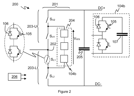
Figure 2 illustrates a voltage source converter (VSC) 200 according to an
embodiment
of the invention. Figure 2 illustrates a phase limb 201 which is connected
between a
high-side DC terminal DC+ and a low-side DC terminal DC- and with an AC
terminal
202. Figure 2 illustrates just one phase limb for clarity but in practice
there may be
multiple, e.g. three, phase limbs, each connected between the high-side and
low-side
DC terminals DC+ and DC- and each having a respective AC terminal.
The phase limb has a phase limb switch arrangement which, in this example,
comprises four switches. The phase limb switch arrangement has first and
second
upper arm switches Sui and SU2 connected in series between the AC terminal 202
and
the high side DC terminal DC+ to form an upper converter arm 203-U. The phase
limb
switch arrangement also has first and second lower arm switches SLi and SL2
connected in series between the AC terminal 202 and the low side DC terminal
DC- to
form a lower converter arm 203-L.
Each of the switches SU1, SU2, SL1, SL2 may be implemented by a suitable
series
connection of switching elements, such as IGBTs 105 and antiparallel diodes
106 as
described previously, e.g. a plurality of series connected switching elements
of the form
104a illustrated in figure 1.
The phase limb also has an associated wave-shaper 204 which is operable, in
use, to
provide a voltage level across its terminals and where the voltage level
provided can be
selectively varied. The voltage wave-shaper may, for instance, comprise a
chain-link
circuit of a plurality of series connected cells 104b such as described above
in relation
to figure 1. As described such cells 104b may comprise an energy storage
element
such as a capacitor 107 and a cell switch arrangement of switching elements,
such as
IGBTs 105 and antiparallel diodes 106 such that the capacitor can be connected
in
series between the cell terminals or bypassed. Figure 2 illustrates that the
cells 104b
of the wave-shaper 204 may have a half bridge cell switch arrangement but in
some
CA 02995538 2018-02-13
WO 2017/029327 PCT/EP2016/069517
12
embodiments a full bridge cell switch arrangement may be used for at least
some of
the cells of the wave-shaper.
The phase limb switch arrangement, e.g. switches SUi, SU2, SLi, SL2, is
operable in a
number of different switch states as may be controlled by a suitable
controller 206. In
particular the phase limb switch arrangement is operable to provide at least
first and
second switch states, where in the first switch state the low-side DC terminal
is
electrically connected to the AC terminal via a first path that includes the
voltage wave-
shaper and in the second switch state the high-side DC terminal is
electrically
connected to the AC terminal via a second path that includes the voltage wave-
shaper.
Figure 3 illustrates the first and second switch states as (1) and (2)
respectively.
In the first switch state (1), switches SL2 and Sui are closed, i.e.
conducting, and
switches SLi and SU2 are open, i.e. non-conducting. This connects the lower
end of the
wave-shaper 204 to the low-side DC terminal and the upper end of the wave-
shaper to
the AC terminal 202. It will be seen that in this switch state the wave-shaper
is
connected in a first path 301 in series between the low-side DC terminal and
the AC
terminal and that the first path includes switch Sui of the upper converter
arm. In this
state the voltage at the AC terminal will be equal to ¨VL + Vws where VL is
the
magnitude of the voltage at the low side terminal (i.e. typically VDc/2) and
Vws is the
present voltage level of the wave-shaper 204.
In the second switch state (2), switches SU2 and SLi are closed, i.e.
conducting, and
switches Sui and SL2 are open, i.e. non-conducting. This connects the upper
end of
the wave-shaper 204 to the high-side DC terminal and the lower end of the wave-
shaper to the AC terminal 202. It will be seen that in this switch state the
wave-shaper
is connected in a second path 302 in series between the high-side DC terminal
and the
AC terminal and that the second path includes switch SLi of the lower
converter arm.
In this state the voltage at the AC terminal will be equal to +VH - Vws where
VH is the
magnitude of the voltage at the high side terminal (i.e. typically VDc/2). It
will be
appreciated that is it the same wave-shaper that is connected in each of the
first and
the second paths.
CA 02995538 2018-02-13
WO 2017/029327 PCT/EP2016/069517
13
If the magnitude of the DC voltage between the terminals is VDC with
IVHI = IVLI = IVDc/21 and the wave-shaper 204 can generate a plurality of
voltage levels
that range from zero to at least +VDc/2, then in the first switch state the
contribution of
the low-side DC voltage at the AC terminal can be varied from ¨VL (i.e.
¨VDc/2) to zero
by varying the voltage of the wave-shaper. Likewise in the second switch state
the
contribution of the high-side DC voltage at the AC terminal can be varied from
+VH (i.e.
+VDc/2) to zero. By appropriately alternating between the first and second
switch
states and varying the voltage of the wave-shaper a desired voltage waveform,
for
instance a trapezoidal waveform may be generated.
Figure 4 illustrates one example of waveforms that may be generated in a phase
limb
such as illustrated in figure 2 using the switch states illustrated in figure
3. For
example, consider that the phase limb is in the first switch state and the
voltage level
Vws of the wave-shaper is zero, such that the voltage at the AC terminal VAC
substantially corresponds to the low-side DC voltage, -VDc/2. The voltage
level of the
wave-shaper 204 may be increased over time (e.g. ramped or stepped) to a level
equal
to VDc/2, at which point the voltage at the AC terminal is substantially zero.
At this
point the phase limb is switched to the second switch state to connect the
high-side
terminal to the AC terminal via the wave-shaper. As the voltage of the wave-
shaper is
equal to +VDc/2 the contribution of the high-side voltage to the voltage at
the AC
terminal at this point in time is zero. The voltage Vws of the wave-shaper can
then be
reduced over time to increase the voltage at the AC terminal, until the
voltage of the
wave-shaper reaches zero and the voltage at the AC terminal is substantially
equal to
the high side voltage +VDc. A period of operation in the first switch state
with an
increasing voltage level of the wave-shaper followed by a period of the second
switch
state with an decreasing voltage level of the wave-shaper thus provides a
continuous
full-scale positive ramp at the AC terminal and can thus be considered a
positive ramp
mode, as it corresponds to a positive ramp of voltage at the AC terminal.
For a trapezoidal waveform the phase limb may then be held in steady state at
this
high voltage level for a period of time. This could be achieved by maintaining
the
second switch state with the voltage level of the wave-shaper held to be zero.
CA 02995538 2018-02-13
WO 2017/029327 PCT/EP2016/069517
14
In some embodiments however the phase limb may instead to be switched at this
point
in time to a different switch state in which the AC terminal is connected to
the high-side
DC terminal via a path that bypasses, i.e. does not include, the wave-shaper.
As
illustrated in figure 3 the phase limb switch arrangement may therefore be
operable in a
third switch state (3) where both of the upper side switches Sui and SU2 are
closed and
both of the lower side switches SLi and SL2 are open and the AC terminal is
connected
to the high side terminal DC+ by a third path 303 that bypasses the wave-
shaper 204.
Likewise the phase limb switch arrangement may also be operable in a fourth
switch
state (4) where both of the upper side switches Sui and SU2 are open and both
of the
lower side switches SLi and SL2 are closed and the AC terminal is connected to
the
low-side terminal DC+ by a fourth path 304 that bypasses the wave-shaper 204.
Referring back to figure 4, after the positive ramp mode reaches the high-side
voltage,
the phase limb may thus be switched to the third state (3) and maintained in
this state
for a period of time. Subsequently a negative ramp mode may then be initiated
which
comprises switching the phase limb to the second switch state and increasing
the
voltage of the wave-shaper to reduce the voltage at the AC terminal to zero,
followed
by, once zero is reached, switching the phase limb to the first switch state
and
decreasing the voltage of the wave-shaper down to zero. At this point in the
time the
AC voltage is thus substantially equal to the low-side voltage and the phase
limb may
be switched to the fourth switch state.
Use of the third and fourth switch states means that the voltage wave-shaper
is only
used during a commutation period where one converter arm of a phase limb is
being
taken out of conduction and the opposite arm brought into conduction. This can
ensure
that the capacitors in each cell of the chain-link forming the wave-shaper see
equal
positive and negative current time areas and can thus help is maintaining
charge
balance of the capacitors.
During the third and fourth switch states the voltage of the wave-shaper may
be
maintained at a non zero voltage, which in this embodiment may be a voltage of
+VDc/2. This can help ensure that the voltage across the converter arm that is
not
conducting is shared between the switches of that converter arm. For example
consider the third state where the upper arm switches Sui and SU2 are closed
so the
CA 02995538 2018-02-13
WO 2017/029327 PCT/EP2016/069517
high-side DC terminal is connected to the AC terminal and the voltage wave-
shaper is
bypassed. In this state the AC terminal will be at a voltage which will be
substantially
the same as the voltage of the high side terminal. Thus the voltage across the
lower
converter arm will be substantially equal to VDC.
5
It will be appreciated however that the node between the switches SLi and SL2
of the
lower converter arm may, in this state, still be connected via the voltage
wave-shaper
to the node between the upper switches Sul and SU2. If there was no voltage
across
the voltage wave-shaper these nodes may thus be at substantially the same
voltage, in
10 other words the voltage at the node between the lower switches would
also be equal to
the high side voltage +VDc/2. This would result in substantially no voltage
across
switch SLi and substantially the whole voltage VDc being applied across switch
SL2.
In this state the voltage of the wave-shaper may thus be maintained at a
voltage equal
15 to +VDc/2. Thus the voltage at the node between the lower converter arm
switches SLi
and SL2 will be at a voltage VDc/2 lower than the high-side voltage, i.e. at
the midrange
voltage. This ensures that there will be a voltage drop of VDc/2 over switch
SLi and
similarly a voltage drop of VDc/2 over switch SL2 so that the voltage
withstand is shared
substantially equally between these switches.
A similar analysis applies for the fourth switch state. Thus in the third and
fourth switch
states the voltage of the wave-shaper may be maintained at a voltage so that
the
voltage of a wave-shaper path between the converter arms is substantially
equal to half
the voltage between the DC terminals.
It can therefore be seen that the same wave-shaper is used during both the
positive
and negative parts of the power cycle to generate (in this example) triangular
waveforms. By switching of the phase limb switch arrangement a trapezoidal
waveform is generated for the AC system. The controller 206 illustrated in
figure 2 may
be arranged to control the switch state of the arm switches and also the cells
of the
chain-link of the wave-shaper 204 to provide this trapezoidal waveform. It
will be
appreciated that the controller 206 is a functional unit and may be
implemented in
practice by a number of individual control elements that may be distributed at
different
levels of the converter in practice.
CA 02995538 2018-02-13
WO 2017/029327 PCT/EP2016/069517
16
If the timings and magnitudes of the trapezoid are correctly determined the
only
components at the AC terminal phase voltage are fundamental and its triplen
frequencies, i.e. the 3rd, 91h harmonic etc. These unwanted triplen harmonic
frequencies can be circulated in a DELTA connected converter transformer
auxiliary
winding (not shown) and thus will not appear in the AC system terminals. The
DC
voltage will be the summation of all phases and will be essentially DC plus
6th harmonic
and its multiples. Various techniques may be used modify the wave-shaper
voltage
output to filter out the 6th harmonic as will be understood from operation of
other types
of VSC.
In some embodiments the basic trapezoidal wave form could be modified to null
other
frequencies including harmonics and non-integer frequency harmonics that may
be
present in the AC and/or DC systems.
In some embodiments, referring back to figure 2, there may be an optional
output
capacitor 205 connected between the DC terminals, which may be used to reduce
the
distortion to the output waveforms.
It should be noted that with the illustrated switching profile of the wave-
shaper, each of
the switches SUi, SU2, SL1, SL2 of the phase limb switching arrangement has an
approximate voltage rating equivalent to half the DC voltage. The wave-shaper
voltage
profile can be changed to modify the DC and AC harmonics but may result in
increases
in the switch voltage ratings.
As mentioned above one voltage wave-shaper is thus effectively shared by both
converter arms of a phase limb. The wave-shaper in the embodiment of figure 2
has a
voltage range from zero to +VDc/2 and can be implemented by a suitable chain-
link of
half-bridge cells. This significantly reduces the number of components
compared to a
conventional MMC type converter, in which each converter arm has a chain-link
with a
voltage rang of VDc or an AAC type converter where each converter arm would
have a
chain-link rated for at least VDc/2. This significantly reduces the number of
cells
required with substantial capacitors and thus results in a converter with a
reduced
CA 02995538 2018-02-13
WO 2017/029327 PCT/EP2016/069517
17
footprint, i.e. size requirement, compared to equivalent converters of
conventional
design.
As shown the wave-shaper may be connected in a wave-shaper path that runs
between an upper node between the first and second upper arm switches and a
lower
node between the first and second lower arm switches.
This arrangement is somewhat similar to a switch arrangement of a known so-
called
flying capacitor converter. In the conventional flying capacitor converter
however a
fixed capacitance is used and arranged so that it can be connected in series
between
either of the DC terminals and the AC terminal or bypassed as required. A
conventional single stage flying capacitor converter thus typically provides
only a single
intermediate voltage between the high-side and low-side voltages. Additional
voltage
levels can be generated by using additional stages with different capacitance
values,
with a pair of switches in each converter arm for selectively including or
bypassing the
flying capacitor stage as required. Such an arrangement requires the use of
multiple
large capacitances of different values and a complex switch arrangement in
each
converter arm which is disadvantageous. Embodiments described herein use a
simple
phase limb switch arrangement and a wave-shaper with a variable voltage level.
In some embodiments however a fixed capacitance may be used in the wave-shaper
path to reduce the voltage range required by the voltage wave-shaper, as
illustrated in
figure 5, in which similar components to those mentioned previously are
identified by
the same reference numerals.
Figure 5 illustrates a wave-shaper 204 connected in series with a fixed
capacitance
501 in a wave-shaper path that extends from a node between the two switches
Sui and
SU2 of the upper arm 203U to a node between the two switches SLi and SU of the
lower
arm 203L. The fixed capacitance 501 is arranged to maintain a substantially
constant
voltage level of say +VDc/4. In this embodiment the wave-shaper is arranged to
provide a variable voltage level that varies between -VDc/4 and +VDc/4. Thus
the
voltage level can be selectively varied between a positive voltage level and a
negative
voltage level and in this example the voltage wave-shaper is operable, in use,
to
CA 02995538 2018-02-13
WO 2017/029327 PCT/EP2016/069517
18
generate a voltage level of equal magnitude and opposite polarity to the
voltage of the
fixed capacitance in use.
When the voltage level of the wave-shaper is equal to -VDc/4 the voltage from
the
wave-shaper and the fixed capacitance together result in a voltage of zero
across the
wave-shaper path. When the voltage level of the wave-shape is zero, only the
voltage
from the fixed capacitance contributes to the voltage across the wave-shaper
path,
which is thus VDc/4. When the voltage level of the wave-shape is equal to
+VDc/4, this
adds to the voltage from the fixed capacitance together to provide a total
voltage of
VDc/2 across the wave-shaper path. Thus voltage across the wave-shaper path
can be
varied between zero and VDc/2, as was the case for the embodiment shown in
figure 2.
The embodiment of figure 5 may be operated in the same way as the embodiment
described with reference to figure 2. Figure 6 illustrates example waveforms
for the
embodiment of figures. The phase limb may be switched to the first switch
state and
the voltage of the wave-shaper increased (i.e. made less negative or more
positive)
from -VDc/4 to +VDc/4 to increase the voltage at the AC terminal from -VDc/2
to zero.
The phase limb may then be switched to the second switch state and the voltage
of the
wave-shaper decreased (i.e. made less positive or more negative) back down to -
VDc/4
to increase the AC voltage from zero to =VDc/2.
As also shown the phase limb may also be connected in a third state where the
upper
switches are both closed and the lower switches are both open and a fourth
switch
state where the upper switches are both open and the lower switches are both
closed.
In the third and fourth states the voltage of the wave-shaper may be
maintained at
+VDc/4 to maintain the voltage of the wave-shaper path at +VDc/2.
The voltage wave-shaper in this example may comprise a chain-link circuit with
cells
502 having a capacitor connected in a full bridge arrangement to allow the
positive and
negative voltages to be derived. This could reduce the number of cells
required for the
chain-link circuit, and hence the number of capacitors required, as the
capacitors of the
chain-link need only provide a voltage range of magnitude VDc/4, albeit
requiring full
bridge cells and the fixed capacitance 501. This still may however use fewer
components that the embodiment of figure 2 and thus represent a further
reduction in
CA 02995538 2018-02-13
WO 2017/029327 PCT/EP2016/069517
19
size compared to a conventional converter design. Alternatively rather than
use a
chain-link converter of full-bridge cells the chain-link itself (which could
be a chain-link
of half-bridge cells) could be connected to the wave-shaper path via a switch
arrangement that allows the chain-link to be selectively connected in series
or anti-
series with the fixed capacitance, i.e. such that the voltage of the wave-
shaper adds to
or acts against that of the fixed capacitance.
The converters described above thus offer operation similar to that of an AAC
type
converter but allow the use of fewer components with a consequent reduction in
cost
and size of the converter and also thus the cost and size of the required
converter
station.
In some embodiments the harmonic content of the AC and/or DC currents may be
improved, e.g. reduced, by providing at least some additional wave-shaping
functionality in a converter arm. Thus in addition to the wave-shaper 204
which is
shared between the converter arm there may be at least one additional wave-
shaper in
each converter arm.
Figure 7 illustrates generally a phase limb of a VSC according to such an
embodiment.
In general the phase limb has a switch arrangement comprising first and second
upper
arm switching blocks 701U and 702U in an upper converter arm and first and
second
upper arm switching blocks 701L and 702L in an upper converter arm. A wave-
shaper
204 is connected in a wave-shaper path that extends between a node of the
upper
converter arm between the first and second upper arm switching blocks 701U and
702U and a node of the lower converter arm between the first and second lower
arm
switching blocks 701L and 702L. The wave-shaper may have any of the forms
described above and/or there may be a fixed capacitance in the wave-shaper
path as
described previously. Note as used herein the term block shall refer to a
functional unit
comprising suitable circuitry.
The arm switching blocks are operable to provide the switch states referred to
above,
e.g. in a first switch state blocks 701U and 702L may be conducting with
blocks 701L
and 702U substantially non-conducting, and in a second switch state blocks
701L and
702U may be conducting with blocks 701U and 702L substantially non-conducting.
CA 02995538 2018-02-13
WO 2017/029327 PCT/EP2016/069517
In some embodiments however both the first upper arm switching block 701U and
the
first lower arm switching block 701L may comprise an in-arm voltage wave-
shaper. For
example such switching blocks may be implemented, at least partly, as a chain-
link
5 circuit with wave-shaping capability. Alternatively both the second upper
arm switching
block 702U and the second lower arm switching block 702L may be implemented,
at
least partly, as a chain-link circuit with wave-shaping capability.
In use the voltage wave-shaper 204 may be controlled as described previously
by a
10 phase limb controller 206 to implement a positive ramp mode or a
negative ramp mode
as required to transition from one converter arm conducting to the other
converter arm
conducting. However in this embodiment in the third or fourth switch states
when the
wave-shaper 204 is bypassed the in-arm wave-shapers, i.e. the chain-links in
each
converter arm, may be controlled to provide voltage waveforms that improves
the
15 harmonic performance of the converter, e.g. by providing a better
approximation of a
sine wave. As such the in-arm wave-shapers may have a relatively limited
voltage
range and thus may comprise only a relatively few cells to provide such a
voltage
range. The in-arm wave-shapers may be controlled by an in-arm wave-shaper
which
may form part of the phase limb controller 206.
The in-arm wave-shapers may also be used to provide a voltage in the first
and/or
second switch states to provide part of the overall voltage differential
between the AC
terminal and the relevant DC terminal. This can help reduce the voltage range
required
for the main wave-shaper 204 and additionally to reduce voltage stress on the
off state
converter arm switches.
The in-arm wave-shapers may comprise a chain-link of full-bridge or half-
bridge cells,
although half bridge cells will give lower conduction losses due to fewer
semiconductor
switches in their implementation. Note if required both of the arm switching
blocks of a
converter arm could be implemented, at least partly, as a chain-link circuit
with wave-
shaping capability.
If at least some of the arm switching blocks do comprise a chain-link with
full-bridge
cells the phase arm may also be able to block DC side faults as will be
understood by
CA 02995538 2018-02-13
WO 2017/029327 PCT/EP2016/069517
21
one skilled in the art, provided that a sufficient rating of full-bridge cells
is provided. It
will be understood that the embodiment illustrated in figures 2 or 5 may lack
the ability
to block at least some DC side fault due to the anti-parallel diodes of the
arm switching
elements providing a conduction path. In such embodiments a separate fault
blocking
element, such as a DC breaker, which may be common to the three phases, may be
provided on the DC side.
In some embodiments a series of wave-shaping cells, which may for example be
full-
bridge cells, may be connected in series with the DC terminals, as illustrated
in figure
8. Figure 8 shows a VSC with three phase limbs 201a, 201b and 201c each
connected
between DC busbars that provide the DC terminals DC+ and DC- and each with a
respective AC terminal 202a-c. Connected in series with the DC terminals, and
thus in
series with each of the phases 201a-c, are busbar wave-shapers comprising a
plurality
of full-bridge cells 801, i.e. a series connection of cells having the general
form 502
illustrated in figures. As illustrated in figure 801 the full-bridge cells 801
may be
connected in series with both high-side and low-side DC terminals.
These full-bridge cells 801 of the busbar wave-shapers can be controlled to
effectively
isolate the DC terminals from the converter at the 61h harmonic frequency. The
wave-
shapers 204 of each phase limb is then controlled then use the resulting DC
plus 3rd
harmonic wave form to construct (near) perfect fundamental frequency sine wave
voltage profiles at the AC terminals of the converter.
Figure 9 illustrates example waveforms for such an embodiment. The full-bridge
cells
in the high-side DC busbar are controlled to create a varying high-side
voltage VH for
the three phases. The variation of the high-side voltage VH is arranged to
correspond
to the voltage variation expected over at least part of the positive half of
each phase
cycle, in this example the peak positive 120 of each phase cycle. The high
side
voltage thus varies by an amount equal to half positive AC voltage, i.e.
+0.5VAc. The
low-side voltage likewise corresponds to a suitable voltage variation for the
peak
negative 120 of each phase cycle, e.g. with a variation equal in magnitude to
half the
peak negative AC voltage, and thus may be out of phase with the variation of
the low-
side voltage by 180 .
CA 02995538 2018-02-13
WO 2017/029327 PCT/EP2016/069517
22
Each phase limb be operated as described previously, e.g. in a repeating
sequence of
switch states (1), (2), (3), (2), (1), (4). In the third switch state however,
when the
wave-shaper for that phase is bypassed and the AC terminal is connected to the
high-
side DC busbar, the variation in the high-side voltage provides the required
voltage
variation. Likewise for the fourth switch state when the AC terminal is
connected to the
low-side DC busbar in a path that bypasses the wave-shaper 204 of that phase
limb.
To transition from the fourth switch state to the third switch state the phase
limb may be
switched to the first switch state and the voltage of the wave-shaper may be
varied
accordingly as described previously.
In this embodiment the wave-shaper may be used in the first and second states
to
provide voltage shaping during the transitions between the third and fourth
states in the
same manner as described previously to generate the desired AC waveform at the
AC
terminal. In this embodiment however the wave-shaper voltage during state 1
needs to
also take into account the modulation of the low-side voltage and likewise in
state 2 the
variation in high-side voltage should be taken into account. During switch
state (1),
where the AC terminal is connected to the low-side DC busbar via the voltage
wave-
shaper the voltage at the AC terminal will be VL + Vws. In this embodiment
however VL
is itself varying and thus the waveform for the wave-shaper will take this
into account.
Figure 9 shows an example of how the voltage Vws may be controlled together
with the
variation in the high-side voltage VH and the low side voltage VL and also the
resulting
AC waveform at the AC terminal. Consider the sequence starting at switch state
(3)
where the AC terminal is connected directly to the high-side DC terminal. The
voltage
of the high-side DC terminal is modulated by the busbar wave-shaper 801 to
provide
the desired voltage variation for this part of the AC cycle for this phase.
The voltage
thus varies from half the positive AC peak voltage to the peak AC voltage and
then
back to half the positive AC peak voltage. At this point the voltage of the
high-side
busbar starts to increase again to provide the required modulation for one of
the other
phases. This phase limb thus switches to switch state (2) where the AC
terminal is
connected to the high-side busbar via the wave-shaper 204 and the voltage of
the
wave-shaper ramps up in a similar fashion as described previously to ramp down
the
voltage at the AC terminal. In this embodiment however the voltage ramp of the
wave-
shaper takes into account the variation of the high-side voltage to provide a
desired AC
CA 02995538 2018-02-13
WO 2017/029327 PCT/EP2016/069517
23
waveform. The voltage of the wave-shaper ramps until the voltage of the AC
voltage is
zero - which occurs at a max ramp voltage, Vm. In this example zero voltage at
the AC
terminal is reached when the high-side voltage VH corresponds to \13/2 of the
peak AC
voltage and this is thus the maximum ramp voltage of the wvae-shaper 204. The
phase limb then switches to state (1) and the wave-shaper voltage ramps down
in a
similar fashion to provide the start of the negative phase until the voltage
at the AC
terminal reach half the peak negative voltage, at which point state (4) is
adopted and
the modulation of the low-side busbar voltage VL provides the necessary
voltage
variation.
In this embodiment during the third and fourth switch states the voltage of
the wave-
shaper may be held at a relatively high voltage to aid in voltage sharing for
the off state
switches of the non-conducting converter arm as described previously. This
could be a
fixed voltage level that is held for the duration of the third or fourth
switch state as
illustrated in figure 9, for instance at a voltage at or around the maximum
ramp voltage.
In some embodiments however the voltage of the wave-shaper could be varied in
accordance with the varying high-side and low-side voltages to maintain equal
sharing
between the off state switches.
It will of course be appreciated that other modulations of the high-side and
low-side
voltages may be implemented and/or different waveforms for the voltage of the
wave-
shaper 204 may be used to provide desired waveforms at the AC terminal.
In the event of a DC pole to pole fault the full-bridge cells 801 can be
switched to block
the flow of the fault current.
Embodiments of the present invention this provide VSCs and method of control
therefore that provide good converter performance by the use of wave-shapers
but
share at least some wave-shaper components between the converter arms of a
phase
limb as required to reduce the number of components required and hence the
cost and
size of the converter.
VSCs of the present invention may be used in HVDC power
distribution/transmission
systems. A first VSC according to an embodiment may be arranged for the
transfer or
CA 02995538 2018-02-13
WO 2017/029327 PCT/EP2016/069517
24
power to/from a second VSC, which may or may not be a VSC according to an
embodiment of the invention. The VSCs could be arranged in a back-to-back
arrangement in the same converter station or the first VSC could be remote
from the
second VSC and connected by a suitable Dc link, for instance via overhead
lines
and/or insulated cables. In some embodiments the first VSC could be part of a
multi-
point network with multiple other VSCs connected to the same DC grid.
It should be noted that the above-mentioned embodiments illustrate rather than
limit
the invention, and that those skilled in the art will be able to design many
alternative
embodiments without departing from the scope of the appended claims. The word
"comprising" does not exclude the presence of elements or steps other than
those
listed in a claim, "a" or "an" does not exclude a plurality, and a single
feature or other
unit may fulfil the functions of several units recited in the claims. Any
reference signs in
the claims shall not be construed so as to limit their scope.