Note: Descriptions are shown in the official language in which they were submitted.
84359347
1
WIRELESS ENERGY TRANSFER SYSTEMS
CROSS-REFERENCE TO RELATED APPLICATIONS
[0001] This application is a divisional of Canadian Patent Application No.
2,738,654 filed on
September 25, 2009. This application claims priority to the following U.S.
patent applications:
[0002] U.S. App. No. 61/100.721 filed September 27, 2008; U.S. App. No.
61/108,743
filed October 27, 2008; U.S. App. No. 61/147,386 filed January 26, 2009; U.S.
App. No.
61/152,086 filed February 12, 2009; U.S. App. No. 61/178,508 filed May 15,
2009; U.S.
App. No. 61/182,768 filed June 1,2009; U.S. App. No. 61/121,159 filed December
9, 2008;
U.S. App. No. 61/142.977 filed January 7, 2009; U.S. App. No. 61/142,885 filed
January 6,
2009; U.S. App. No. 61/142,796 filed January 6, 2009; U.S. App. No. 61/142,889
filed
January 6, 2009; U.S. App. No. 61/142,880 filed January 6, 2009; U.S. App. No.
61/142,818
filed January 6, 2009; U.S. App. No. 61/142.887 tiled January 6, 2009; U.S.
App. No.
61/156,764 filed March 2,2009; U.S. App. No. 61/143,058 filed January 7,2009;
U.S. App.
No. 61/152,390 filed February 13, 2009: U.S. App. No. 61/163,695 filed March
26, 2009;
U.S. App. No. 61/172,633 filed April 24, 2009; U.S. App. No. 61/169.240 filed
April 14,
2009, and U.S. App. No. 61/173,747 filed April 29, 2009.
BACKGROUND
[0003] Field:
[0004] This disclosure relates to wireless energy transfer, also referred
to as wireless
power transmission.
[0005] Description of the Related Art:
[0006] Energy or power may be transferred wirelessly using a variety of
known
radiative, or far-field, and non-radiative, or near-field. techniques. For
example, radiative
wireless information transfer using low-directionality antennas, such as those
used in radio
and cellular communications systems and home computer networks, may be
considered
wireless energy transfer. However, this type of radiative transfer is very
inefficient because
only a tiny portion of the supplied or radiated power, namely, that portion in
the direction of,
and
CA 3011548 2018-07-17
=
10. WO 2010/036980
PCMS2009/058499 =
2
overlapping with, the receiver is picked up. The vast majority of the power is
radiated away in all
the other directions and lost in free space. Such inefficient power transfer
may be acceptable for
data transmission, but is not practical for transferring useful amounts of
electrical energy for the
purpose of doing work, such as for powering or charging electrical devices.
One way to improve
the transfer efficiency of some radiative energy transfer schemes is to use
directional antennas to
confine and preferentially direct the radiated energy towards a receiver.
However, these directed
radiation schemes may require an uninterruptible line-of-sight and potentially
complicated
tracking and steering mechanisms in the case of mobile transmitters and/or
receivers. In addition,
such schemes may pose hazards to objects or people that cross or intersect the
beam when
modest to high amounts of power are being transmitted. A known non-radiative,
or near-field,
wireless energy transfer scheme, often referred to as either induction or
traditional induction,
does not (intentionally) radiate power, but uses an oscillating current
passing through a primary
coil, to generate an oscillating magnetic near-field that induces currents in
a near-by receiving or
secondary coil. Traditional induction schemes have demonstrated the
transmission of modest to
large amounts of power, however only over very short distances, and with very
small offset
tolerances between the primary power supply unit and the secondary receiver
unit. Electric
transformers and proximity chargers are examples of devices that utilize this
known short range,
near-field energy transfer scheme.
[00071 Therefore a need exists for a wireless power transfer scheme
that is capable of
transferring useful amounts of electrical power over mid-range distances or
alignment offsets.
Such a wireless power transfer scheme should enable useful energy transfer
over greater
distances and alignment offsets than those realized with traditional induction
schemes, but
without the limitations and risks inherent in radiative transmission schemes.
SUMMARY
[00081 There is disclosed herein a non-radiative or near-field
wireless energy transfer
scheme that is capable of transmitting useful amounts of power over mid-range
distances and
alignment offsets. This inventive technique uses coupled electromagnetic
resonators with long-
lived oscillatory resonant modes to transfer power from a power supply to a
power drain. The
technique is general and may be applied to a wide range of resonators, even
where the specific
examples disclosed herein relate to electromagnetic resonators. If the
resonators are designed
CA 3011548 2018-07-17
41111 WO 2010/036980 PCT/US2009/058499
3
such that the energy stored by the electric field is primarily confined within
the structure and that
the energy stored by the magnetic field is primarily in the region surrounding
the resonator.
Then, the energy exchange is mediated primarily by the resonant magnetic near-
field. These
types of resonators may be referred to as magnetic resonators. If the
resonators are designed such
that the energy stored by the magnetic field is primarily confined within the
structure and that the
energy stored by the electric field is primarily in the region surrounding the
resonator. Then, the
energy exchange is mediated primarily by the resonant electric near-field.
These types of
resonators may be referred to as electric resonators. Either type of resonator
may also be referred
to as an electromagnetic resonator. Both types of resonators are disclosed
herein.
[00091 The omni-directional but stationary (non-lossy) nature of the
near-fields of the
resonators we disclose enables efficient wireless energy transfer over mid-
range distances, over a
wide range of directions and resonator orientations, suitable for charging,
powering, or
simultaneously powering and charging a variety of electronic devices. As a
result, a system may
have a wide variety of possible applications where a first resonator,
connected to a power source,
is in one location, and a second resonator, potentially connected to
electrical/electronic devices,
batteries, powering or charging circuits, and the like, is at a second
location, and where the
distance from the first resonator to the second resonator is on the order of
centimeters to meters.
For example, a first resonator connected to the wired electricity grid could
be placed on the
ceiling of a room, while other resonators connected to devices, such as
robots, vehicles,
computers, communication devices, medical devices, and the like, move about
within the room,
and where these devices are constantly or intermittently receiving power
wirelessly from the
source resonator. From this one example, one can imagine many applications
where the systems
and methods disclosed herein could provide wireless power across mid-range
distances,
including consumer electronics, industrial applications, infrastructure power
and lighting,
transportation vehicles, electronic games, military applications, and the
like.
[0010] Energy exchange between two electromagnetic resonators can be
optimized
when the resonators are tuned to substantially the same frequency and when the
losses in the
system are minimal. Wireless energy transfer systems may be designed so that
the "coupling-
time" between resonators is much shorter than the resonators' "loss-times".
Therefore, the
systems and methods described herein may utilize high quality factor (high-Q)
resonators with
low intrinsic-loss rates. In addition, the systems and methods described
herein may use sub-
CA 3011548 2018-07-17
= WO 2010/036980 PCT/US2009/058499 =
4
wavelength resonators with near-fields that extend significantly longer than
the characteristic
sizes of the resonators, so that the near-fields of the resonators that
exchange energy overlap at
mid-range distances. This is a regime of operation that has not been practiced
before and that
differs significantly from traditional induction designs.
100111 It is important to appreciate the difference between the high-Q
magnetic
resonator scheme disclosed here and the known close-range or proximity
inductive schemes,
namely, that those known schemes do not conventionally utilize high-Q
resonators. Using
coupled-mode theory (CMT), (see, for example, Waves and Fields in
Optoelectronics, H.A.
Haus, Prentice Hall, 1984), one may show that a high-Q resonator-coupling
mechanism can
enable orders of magnitude more efficient power delivery between resonators
spaced by mid-
range distances than is enabled by traditional inductive schemes. Coupled high-
Q resonators
have demonstrated efficient energy transfer over mid-range distances and
improved efficiencies
and offset tolerances in short range energy transfer applications.
[0012] The systems and methods described herein may provide for near-
field wireless
energy transfer via strongly coupled high-Q resonators, a technique with the
potential to transfer
power levels from picowatts to kilowatts, safely, and over distances much
larger than have been
achieved using traditional induction techniques. Efficient energy transfer may
be realized for a
variety of general systems of strongly coupled resonators, such as systems of
strongly coupled
acoustic resonators, nuclear resonators, mechanical resonators, and the like,
as originally
described by researchers at M.I.T. in their publications, "Efficient wireless
non-radiative mid-
range energy transfer", Annals of Physics, vol. 323, Issue 1, p. 34 (2008) and
"Wireless Power
Transfer via Strongly Coupled Magnetic Resonances", Science, vol. 317, no.
5834, p. 83, (2007).
Disclosed herein are electromagnetic resonators and systems of coupled
electromagnetic
resonators, also referred to more specifically as coupled magnetic resonators
and coupled electric
resonators, with operating frequencies below 10 GHz.
[0013] This disclosure describes wireless energy transfer technologies,
also referred
to as wireless power transmission technologies. Throughout this disclosure, we
may use the
terms wireless energy transfer, wireless power transfer, wireless power
transmission, and the
like, interchangeably. We may refer to supplying energy or power from a
source, an AC or DC
source, a battery, a source resonator, a power supply, a generator, a solar
panel, and thermal
collector, and the like, to a device, a remote device, to multiple remote
devices, to a device
CA 3011548 2018-07-17
= WO 2010/036980 PCT/IIS2009/058499 0
resonator or resonators, and the like. We may describe intermediate resonators
that extend the
range of the wireless energy transfer system by allowing energy to hop,
transfer through, be
temporarily stored, be partially dissipated, or for the transfer to be
mediated in any way, from a
source resonator to any combination of other device and intermediate
resonators, so that energy
transfer networks, or strings, or extended paths may be realized. Device
resonators may receive
energy from a source resonator, convert a portion of that energy to electric
power for powering
or charging a device, and simultaneously pass a portion of the received energy
onto other device
or mobile device resonators. Energy may be transferred from a source resonator
to multiple
device resonators, significantly extending the distance over which energy may
be wirelessly
transferred_ The wireless power transmission systems may be implemented using
a variety of
system architectures and resonator designs. The systems may include a single
source or multiple
sources transmitting power to a single device or multiple devices. The
resonators may be
designed to be source or device resonators, or they may be designed to be
repeaters. In some
cases, a resonator may be a device and source resonator simultaneously, or it
may be switched
from operating as a source to operating as a device or a repeater. One skilled
in the art will
understand that a variety of system architectures may be supported by the wide
range of
resonator designs and functionalities described in this application.
[0014] In the wireless energy transfer systems we describe, remote
devices may be
powered directly, using the wirelessly supplied power or energy, or the
devices may be coupled
to an. energy storage unit such as a battery, a super-capacitor, an ultra-
capacitor, or the like (or
other kind of power drain), where the energy storage unit may be charged or re-
charged
wirelessly, anclior where the wireless power transfer mechanism is simply
supplementary to the
main power source of the device_ The devices may be powered by hybrid
battery/energy storage
devices such as batteries with integrated storage capacitors and the like.
Furthermore, novel
battery and energy storage devices may be designed to take advantage of the
operational
improvements enabled by wireless power transmission systems_
[00151 Other power management scenarios include using wirelessly
supplied power
to recharge batteries or charge energy storage units while the devices they
power are turned off',
in an idle state, in a sleep mode, and the like. Batteries or energy storage
units may be charged or
recharged at high (fast) or low (slow) rates. Batteries or energy storage
units may be trickle
charged or float charged. Multiple devices may be charged or powered
simultaneously in parallel
CA 3011548 2018-07-17
WO 2010/036980
PCMS2009/058499 =
6
or power delivery to multiple devices may be serialized such that one or more
devices receive
power for a period of time after which other power delivery is switched to
other devices_
Multiple devices may share power from one or more sources with one or more
other devices
either simultaneously, or in a time multiplexed manner, or in a frequency
multiplexed manner, or
in a spatially multiplexed manner, or in an orientation multiplexed manner, or
in any
combination of time and frequency and spatial and orientation multiplexing.
Multiple devices
may share power with each other, with at least one device being reconfigured
continuously,
intermittently, periodically, occasionally, or temporarily, to operate as
wireless power sources. It
would be understood by one of ordinary skill in the art that there are a
variety of ways to power
and/or charge devices, and the variety of ways could be applied to the
technologies and
applications described herein.
[0016] Wireless energy transfer has a variety of possible applications
including for
example, placing a source (e.g. one connected to the wired electricity grid)
on the ceiling, under
the floor, or in the walls of a room, while devices such as robots, vehicles,
computers, PDAs or
similar are placed or move freely within the room. Other applications may
include powering or
recharging electric-engine vehicles, such as buses and/or hybrid cars and
medical devices, such
as wearable or implantable devices. Additional example applications include
the ability to power
or recharge autonomous electronics (e.g. laptops, cell-phones, portable music
players, house-
hold robots, UPS navigation systems, displays, etc), sensors, industrial and
manufacturing
equipment, medical devices and monitors, home appliances and tools (e.g.
lights, fans, drills,
saws, heaters, displays, televisions, counter-top appliances, etc.), military
devices, heated or
illuminated clothing, communications and navigation equipment, including
equipment built into
vehicles, clothing and protective-wear such as helmets, body armor and vests,
and the like, and
the ability to transmit power to physically isolated devices such as to
implanted medical devices,
to hidden, buried, implanted or embedded sensors or tags, to and/or from roof-
top solar panels to
indoor distribution panels, and the like.
[0017] In one aspect, a system disclosed herein includes a source
resonator having a
Q-factor Qi and a characteristic size xi, coupled to a power generator, and a
second resonator
having a Q-factor Q2 and a characteristic size x2, coupled to a load located a
distance D from the
source resonator, wherein the source resonator and the second resonator arc
coupled to exchange
CA 3011548 2018-07-17
= WO 2010/036980 PCT/US2009/058499 =
7
energy wirelessly among the source resonator and the second resonator, and
wherein V2Q2 >
100.
[00181 Q/ may be less than 100. Q2 may be less than 100. The system may
include a
third resonator having a Q-factor Q3 configured to transfer energy non-
raditively with the source
QQ
and second resonators ,wherein 1Q1Q3> 100 V2, >100 and .. . Q3 may be less
than 100.
[00191 The source resonator may be coupled to the power generator with
direct
electrical connections. The system may include an impedance matching network
wherein the
source resonator is coupled and impedance matched to the power generator with
direct electrical
connections. The system may include a tunable circuit wherein the source
resonator is coupled to
the power generator through the tunable circuit with direct electrical
connections. The tunable
circuit may include variable capacitors. The tunable circuit may include
variable inductors. At
least one of the direct electrical connections may be configured to
substantially preserve a
resonant mode of the source resonator. The source resonator may have a first
terminal, a second
terminal, and a center terminal, and an impedance between the first terminal
and the center
terminal and between the second terminal and the center terminal may be
substantially equal.
The source resonator may include a capacitive loaded loop having a first
terminal, a second
terminal, and a center terminal, wherein an impedance between the first
terminal and the center
terminal and between the second terminal and the center terminal are
substantially equal. The
source resonator may be coupled to an impedance matching network and the
impedance
matching network further comprises a first terminal, a second terminal, and a
center terminal,
wherein an impedance between the first terminal and the center terminal and
between the second
terminal and the center terminal are substantially equal.
[0020] The first terminal and the second terminal may be directly
coupled to the
power generator and driven with oscillating signals that are near 180 degrees
out of phase_ The
source resonator may have a resonant frequency ro, and the first terminal and
the second
terminal may be directly coupled to the power generator and driven with
oscillating signals that
are substantially equal to the resonant frequency ai . The center terminal may
be connected to an
electrical ground. The source resonator may have a resonant frequency co, and
the first terminal
and the second terminal may be directly coupled to the power generator and
driven with a
CA 3011548 2018-07-17
ILA
150412-4717
8
frequency substantially equal to the resonant frequency a), . The system may
include a plurality
of capacitors coupled to the power generator and the load. The source
resonator and the second
resonator may each be enclosed in a low loss tangent material. The system may
include a power
conversion circuit wherein the second resonator is coupled to the power
conversion circuit to
deliver DC power to the load. The system may include a power conversion
circuit wherein the
second resonator is coupled to the power conversion circuit to deliver AC
power to the load. The
system may include a power conversion circuit, wherein the second resonator is
coupled to the
power conversion circuit to deliver both AC and DC power to the load. The
system may include
a power conversion circuit and a plurality of loads, wherein the second
resonator is coupled to
= the power conversion circuit, and the power conversion circuit is coupled
to the plurality of
loads. The impedance matching network may include capacitors. The impedance
matching
network may include inductors.
100211 Throughout this disclosure we may refer to the certain
circuit components
such as capacitors, inductors, resistors, diodes, switches and the like as
circuit components or
= elements. We may also refer to series and parallel combinations of these
components as
elements, networks, topologies, circuits, and the like. We may describe
combinations of
capacitors, diodes, varactors, transistors, and/or switches as adjustable
impedance networks,
tuning networks, matching networks, adjusting elements, and the like. We may
also refer to
"self-resonant÷ objects that have both capacitance, and inductance distributed
(or partially
distributed, as opposed to solely lumped) throughout the entire object. It
would be understood by
one of ordinary skill in the art that adjusting and controlling variable
components within a circuit
or network may adjust the performance of that circuit or network and that
those adjustments may
be described generally as tuning, adjusting, matching, correcting, and the
like. Other methods to
tune or adjust the operating point of the wireless power transfer system may
be used alone, or in
addition to adjusting tunable components such as inductors and capacitors, or
banks of inductors
and capacitors.
[00221 Unless otherwise defined, all technical and scientific
terms used herein have
the same meaning as commonly understood by one of ordinary skill in the art to
which this
disclosure belongs. In case of conflict with publications, patent
applications, patents, and other
references mentioned, the present specification, including definitions, will
control.
CA 3011548 2018-07-17
84359347
8a
[0022a] According to one aspect of the present invention, there is
provided a
method, comprising: adjusting an impedance matching network coupled to a power
source in
a wireless power transfer system to compensate for a change in an electrical
load coupled to a
power receiving device of the wireless power transfer system, the impedance
matching
network comprising: a first inductive element formed by at least one loop of
electrically
conductive material; a first adjustable capacitor connected in series with the
first inductive
element to form a first circuit pathway; a second adjustable capacitor
connected in parallel to
the first circuit pathway and forming a second circuit pathway; and a second
adjustable
inductive element connected in series with the first and second circuit
pathways, wherein the
first inductive element forms a portion of a high-Q resonator having an
intrinsic Q value
greater than 100 for at least one resonant frequency between 10 kHz and 100
MHz; and
wherein adjusting the impedance matching network comprises adjusting at least
one of a
capacitance value of the first adjustable capacitor, a capacitance value of
the second
adjustable capacitor, and an inductance value of the second adjustable
inductive element.
[0022b] According to another aspect of the present invention, there
is provided
a wireless power system for powering a device, the system comprising: at least
one device
resonator comprising at least one loop of conductive material; a matching
network coupled
with the at least one loop of conductive material, wherein the device
resonator and the
matching network comprise at least two capacitive elements: and power and
control circuitry
coupled with the matching network at two terminals and configured to connect
with a load of
the device, wherein the matching network is configured to provide voltages of
equal
magnitude and opposite sign at the terminals when coupling power from the at
least one
device resonator to the power and control circuitry; and wherein the at least
one device
resonator is configured to wirelessly receive power from a source resonator
via an oscillating
magnetic field generated by the source resonator.
[0022c] According to still another aspect of the present
invention,
there is provided an apparatus comprising: a device having a load; at least
one device
resonator comprising at least one loop of conductive material; a matching
network coupled
with the at least one loop of conductive material and wherein the resonator
and the
CA 3011548 2018-07-17
84359347
8b
matching network comprise at least two capacitive elements; and power and
control
circuitry coupled with the matching network at two terminals and configured to
connect
with the load of the device, wherein the matching network is configured to
provide
voltages of equal magnitude and opposite sign at the terminals when coupling
power from
the at least one device resonator to the power and control circuitry; and
wherein the at least
one device resonator is configured to wirelessly receive power from a source
resonator via
an oscillating magnetic field generated by the source resonator.
CA 3011548 2018-07-17
SIOW WO 2010/036980 PCT/US2009/058499
9
[0023] .. Any of the features described above may be used, alone or in
combination,
without departing from the scope of this disclosure. Other features, objects,
and advantages of
the systems and methods disclosed herein will be apparent from the following
detailed
description and figures.
BRIEF DESCRIPTION OF FIGURES
[0024] .. Fig. 1 (a) and (b) depict exemplary wireless power systems
containing a
source resonator 1 and device resonator 2 separated by a distance D.
[0025] Fig. 2 shows an exemplary resonator labeled according to the
labeling
convention described in this disclosure. Note that there are no extraneous
objects or additional
resonators shown in the vicinity of resonator 1.
[0026] Fig_ 3 shows an exemplary resonator in the presence of a "loading"
object,
labeled according to the labeling convention described in this disclosure.
[00271 Fig. 4 shows an exemplary resonator in the presence of a
"perturbing" object,
labeled according to the labeling convention described in this disclosure.
[0028] .. Fig. 5 shows a plot of efficiency, i, vs. strong coupling factor,
U= =
[0029] Fig. 6 (a) shows a circuit diagram of one example of a resonator (b)
shows a
diagram of one example of a capacitively-loaded inductor loop magnetic
resonator, (c) shows a
drawing of a self-resonant coil with distributed capacitance and inductance,
(d) shows a
simplified drawing of the electric and magnetic field lines associated with an
exemplary
magnetic resonator of the current disclosure, and (e) shows a diagram of one
example of an
electric resonator.
[0030] .. Fig. 7 shows a plot of the "quality factor", Q (solid line), as a
function of
frequency, of an exemplary resonator that may be used for wireless power
transmission at MHz
frequencies. The absorptive Q (dashed line) increases with frequency, while
the radiative Q
(dotted line) decreases with frequency, thus leading the overall Q to peak at
a particular
frequency.
[0031] Fig. 8 shows a drawing of a resonator structure with its
characteristic size,
thickness and width indicated.
[0032] Fig. 9 (a) and (b) show drawings of exemplary inductive loop
elements.
CA 3011548 2018-07-17
84359347
[00331 Fig. 10 (a) and (b) show two examples of trace structures
formed on printed
circuit boards and used to realize the inductive element in magnetic resonator
structures.
[00341 Fig. 1 I (a) shows a perspective view diagram of a planar
magnetic resonator,
(b) shows a perspective view diagram of a two planar magnetic resonator with
various
geometries, and c) shows a perspective view diagram of a two planar magnetic
resonators
separated by a distance D.
[0035] Fig. 12 is a perspective view of an example of a planar
magnetic resonator.
[00361 Fig. 13 is a perspective view of a planar magnetic resonator
arrangement with
a circular resonator coil.
[0037] Fig. 14 is a perspective view of an active area of a planar
magnetic resonator.
[0038] Fig. 15 is a perspective view of an application of the wireless
power transfer
system with a source at the center of a table powering several devices placed
around the source.
[0039] Fig. 16(a) shows a 3D finite element model of a copper and
magnetic material
structure driven by a square loop of current around the choke point at its
center. In this example,
a structure may be composed of two boxes made of a conducting material such as
copper,
covered by a layer of magnetic material, and connected by a block of magnetic
material. The
inside of the two conducting boxes in this example would be shielded from AC
electromagnetic
fields generated outside the boxes and may house lossy objects that might
lower the Q of the
resonator or sensitive components that might be adversely affected by the AC
electromagnetic
fields. Also shown are the calculated magnetic field streamlines generated by
this structure,
indicating that the magnetic field lines tend to follow the lower reluctance
path in the magnetic
material. Fig. 16(b) shows interaction, as indicated by the calculated
magnetic field streamlines,
between two identical structures as shown in (a). Because of symmetry, and to
reduce
computational complexity, only one half of the system is modeled (but the
computation assumes
the symmetrical arrangement of the other half).
[00401 Fig. 17 shows an equivalent circuit representation of a
magnetic resonator
including a conducting wire wrapped /Vtimes around a structure, possibly
containing
magnetically permeable material. The inductance is realized using conducting
loops wrapped
around a structure comprising a magnetic material and the resistors represent
loss mechanisms in
the system (Rwirc for resistive losses in the loop, RI, denoting the
equivalent series resistance of
the structure surrounded by the loop). Losses may be minimized-to realize high-
Q resonators.
CA 3011548 2019-11-28
WO 2010/036980 PCT/US2009/058499 1111
11
[0041] Fig. 18 shows a Finite Element Method (FEM) simulation of two
high
conductivity surfaces above and below a disk composed of lossy dielectric
material, in an
external magnetic field of frequency 6.78 MHz. Note that the magnetic field
was uniform before
the disk and conducting materials were introduced to the simulated
environment. This simulation
is performed in cylindrical coordinates. The image is azimuthally symmetric
around the r=
axis. The lossy dielectric disk has e.f. = 1 and 0-= 10 S/m.
[0042] Fig. 19 shows a drawing of a magnetic resonator with a lossy
object in its
vicinity completely covered by a high-conductivity surface.
[0043] Fig. 20 shows a drawing of a magnetic resonator with a lossy
object in its
vicinity partially covered by a high-conductivity surface.
[0044] Fig. 21 shows a drawing of a magnetic resonator with a lossy
object in its
vicinity placed on top of a high-conductivity surface.
[0045] Fig. 22 shows a diagram of a completely wireless projector.
[0046] Fig. 23 shows the magnitude of the electric and magnetic fields
along a line
that contains the diameter of the circular loop inductor and along the axis of
the loop inductor.
[0047] Fig. 24 shows a drawing of a magnetic resonator and its
enclosure along with
a necessary but lossy object placed either (a) in the corner of the enclosure,
as far away from the
resonator structure as possible or (b) in the center of the surface enclosed
by the inductive
element in the magnetic resonator.
[0048] Fig. 25 shows a drawing of a magnetic resonator with a high-
conductivity
surface above it and a lossy object, which may be brought into the vicinity of
the resonator, but
above the high-conductivity sheet.
[0049] Fig. 26(a) shows an axially symmetric FEM simulation of a thin
conducting
(copper) cylinder or disk (20 cm in diameter, 2 cm in height) exposed to an
initially uniform,
externally applied magnetic field (gray flux lines) along the z-axis. The axis
of symmetry is at
r=0. The magnetic streamlines shown originate at z = ¨w, where they are spaced
from r=3 cm to
r=10 cm in intervals of 1 cm. The axes scales are in meters. Fig. 26 (b) shows
the same structure
and externally applied field as in (a), except that the conducting cylinder
has been modified to
include a 0.25 mm layer of magnetic material (not visible) with u.=40, on its
outside surface.
Note that the magnetic streamlines are deflected away from the cylinder
significantly less than in
(a).
CA 3011548 2018-07-17
=
WO 2010/036980 PC11082009/058499
12
[00501 Fig. 27 shows an axi-symmetric view of a variation based on the
system
shown in Fig. 26. Only one surface of the lossy material is covered by a
layered structure of
copper and magnetic materials. The inductor loop is placed on the side of the
copper and
magnetic material structure opposite to the lossy material as shown.
[0051] Fig. 28 (a) depicts a general topology of a matching circuit
including an
indirect coupling to a high-Q inductive element.
[0052] Fig. 28 (b) shows a block diagram of a magnetic resonator that
includes a
conductor loop inductor and a tunable impedance network. Physical electrical
connections to this
resonator may be made to the terminal connections.
[0053] Fig. 28 (c) depicts a general topology of a matching circuit
directly coupled to
a high-Q inductive element.
[0054] Fig. 28 (d) depicts a general topology of a symmetric matching
circuit directly
coupled to a high-Q inductive element and driven anti-symmetrically (balanced
drive).
[0055] Fig. 28 (e) depicts a general topology of a matching circuit
directly coupled to
a high-Q inductive element and connected to ground at a point of symmetry of
the main
resonator (unbalanced drive).
[0056) Figs. 29(a) and 29(b) depict two topologies of matching circuits
transformer-
coupled (Le. indirectly or inductively) to a high-Q inductive element. The
highlighted portion of
the Smith chart in (c) depicts the complex impedances (arising from L and R of
the inductive
element) that may be matched to an arbitrary real impedance Zo by the topology
of Fig. 31(b) in
the case w1,2=1/0)C2.
[0057] Figs. 30(a),(b),(c),(d),(e),(f) depict six topologies of
matching circuits directly
coupled to a high-Q inductive element and including capacitors in series with
Zo. The topologies
shown in Figs. 30(a),(b),(c) are driven with a common-mode signal at the input
terminals, while
the topologies shown in Figs 30(d),(e),(f) are symmetric and receive a
balanced drive. The
highlighted portion of the Smith chart in 30(g) depicts the complex impedances
that may be
matched by these topologies. Figs. 30(h),(i),(j),(k),(1),(m) depict six
topologies of matching
circuits directly coupled to a high-Q inductive element and including
inductors in series with Zo.
[0058] Figs. 31(a),(b),(c) depict three topologies of matching circuits
directly coupled
to a high-Q inductive element and including capacitors in series with Zo. They
are connected to
ground at the center point of a capacitor and receive an unbalanced drive. The
highlighted
CA 3011548 2018-07-17
WO 20101036980
PCT/US2009/058499 -11/
13
portion of the Smith chart in Fig. 31.(d) depicts the complex impedances that
may be matched by
these topologies. Figs. 31(e),(0,(g) depict three topologies of matching
circuits directly coupled
to a high-Q inductive element and including inductors in series with Zo.
[00591 Figs. 32(a),(b),(c) depict three topologies of matching circuits
directly coupled
to a high-Q inductive element and including capacitors in series with Zo. They
are connected to
ground by tapping at the center point of the inductor loop and receive an
unbalanced drive. The
highlighted portion of the Smith chart in (d) depicts the complex impedances
that may be
matched by these topologies, (e),(f),(g) depict three topologies of matching
circuits directly
coupled to a high-Q inductive element and including inductors in series with
Zo.
[00601 Figs. 33(a),(b),(c),(d),(e),(f) depict six topologies of
matching circuits directly
coupled to a high-Q inductive element and including capacitors in parallel
with Ze. The
topologies shown in Figs. 33(a),(b),(c) arc driven with a common-mode signal
at the input
terminals, while the topologies shown in Figs 33(d),(e),(f) are symmetric and
receive a balanced
drive. The highlighted portion of the Smith chart in Fig. 33(g) depicts the
complex impedances
that may be matched by these topologies. Figs. 33(h),(i),(j),(k),(1),(m)
depict six topologies of
matching circuits directly coupled to a bigh-Q inductive element and including
inductors in
parallel with 4.
[00611 Figs. 34(a),(b),(c) depict three topologies of matching circuits
directly coupled
to a high-Q inductive element and including capacitors in parallel with Zo.
They are connected to
ground at the center point of a capacitor and receive an unbalanced drive. The
highlighted
portion of the Smith chart in (d) depicts the complex impedances that may be
matched by these
topologies. Figs. 34(e),(f),(g) depict three topologies of matching circuits
directly coupled to a
high-Q inductive element and including inductors in parallel with Zo.
[0062] Figs. 35(a),(b),(c) depict three topologies of matching circuits
directly coupled
to a high-Q inductive element and including capacitors in parallel with Zo.
They are connected to
ground by tapping at the center point of the inductor loop and receive an
unbalanced drive. The
highlighted portion of the Smith chart in Figs. 35(d),(e), and (f) depict the
complex impedances
that may be matched by these topologies.
[0063] Figs. 36(a),(b),(c),(d) depict four topologies of networks of
fixed and variable
capacitors designed to produce an overall variable capacitance with finer
tuning resolution and
some with reduced voltage on the variable capacitor.
CA 3011548 2018-07-17
= WO 2010/036980 PCT/IIS2009/058499 =
14
[0064) Figs_ 37(a) and 37(b) depict two topologies of networks of fixed
capacitors
and a variable inductor designed to produce an overall variable capacitance.
[0065) Fig. 38 depicts a high level block diagram of a wireless power
transmission
system.
[0066] Fig. 39 depicts a block diagram of an exemplary wirelessly
powered device.
100671 Fig. 40 depicts a block diagram of the source of an exemplary
wireless power
transfer system.
[00681 Fig. 41 shows an equivalent circuit diagram of a magnetic
resonator. The slash
through the capacitor symbol indicates that the represented capacitor may be
fixed or variable.
The port parameter measurement circuitry may be configured to measure certain
electrical
signals and may measure the magnitude and phase of signals.
[0069] Fig. 42 shows a circuit diagram of a magnetic resonator where
the tunable
impedance network is realized with voltage controlled capacitors. Such an
implementation may
be adjusted, tuned or controlled by electrical circuits including programmable
or controllable
voltage sources and]or computer pmcessors. The voltage controlled capacitors
may be adjusted
in response to data measured by the port parameter measurement circuitry and
processed by
measurement analysis and control algorithms and hardware. The voltage
controlled capacitors
may be a switched bank of capacitors.
[0070] Fig. 43 shows an. end-to-end wireless power transmission system.
In this
example, both the source and the device contain port measurement circuitry and
a processor. The
box labeled "coupler/switch" indicates that the port measurement circuitry may
be connected to
the resonator by a directional coupler or a switch, enabling the measurement,
adjustment and
control of the source and device resonators to take place in conjunction with,
or separate from,
the power transfer functionality.
[00711 Fig. 44 shows an end-to-end wireless power transmission system.
In this
example, only the source contains port measurement circuitry and a processor.
In this case, the
device resonator operating characteristics may be fixed or may be adjusted by
analog control
circuitry and without the need for control signals generated by a processor.
[0072] Fig. 45 shows an end-to-end wireless power transmission system.
In this
example, both the source and the device contain port measurement circuitry but
only the source
contains a processor. Data from the device is transmitted through a wireless
communication
CA 3011548 2018-07-17
41, WO 2010/036980
PCT/US2009/058499 =
channel, which could be implemented either with a separate antenna, or through
some
modulation of the source drive signal.
[00731 Fig. 46 shows an end-to-end wireless power transmission system.
In this
example, only the source contains port measurement circuitry and a processor.
Data from the
device is transmitted through a wireless communication channel, which could be
implemented
either with a separate antenna, or through some modulation of the source drive
signal.
[0074] Fig. 47 shows coupled magnetic resonators whose frequency and
impedance
may be automatically adjusted using algorithms implemented using a processor
or a computer.
[0075] Fig. 48 shows a varactor array.
[00761 Fig. 49 shows a device (laptop computer) being wirelessly powered
or
charged by a source, where both the source and device resonator are physically
separated from,
but electrically connected to, the source and device.
[0077] Fig. 50 (a) is an illustration of a wirelessly powered or charged
laptop
application where the device resonator is inside the laptop case and is not
visible.
10078I Fig. 50 (b) is an illustration of a wirelessly powered or charged
laptop
application where the resonator is underneath the laptop base and is
electrically connected to the
laptop power input by an electrical cable.
[00791 Fig. 50 (c) is an illustration of a wirelessly powered or charged
laptop
application where the resonator is attached to the laptop base.
[0080] Fig. 50 (d) is an illustration of a wirelessly powered or charged
laptop
application where the resonator is attached to the laptop display.
[0081] Fig. 51 is a diagram of rooftop PV panels with wireless power
transfer.
DETAILED DESCRIPTION
[0082] As described above, this disclosure relates to coupled
electromagnetic
resonators with long-lived oscillatory resonant modes that may wirelessly
transfer power from a
power supply to a power drain. However, the technique is not restricted to
electromagnetic
resonators, but is general and may be applied to a wide variety of resonators
and resonant
objects. Therefore, we first describe the general technique, and then disclose
electromagnetic
examples for wireless energy transfer.
[0083] Resonators
CA 3011548 2018-07-17
= WO 20101036980
PCT/US2009/058499 =
16
[0084] A resonator may be defined as a system that can store energy in
at least two
different forms, and where the stored energy is oscillating between the two
forms. The resonance
has a specific oscillation mode with a resonant (modal) frequency,f; and a
resonant (modal)
field. The angular resonant frequency, co, may be defined as co= 22rf the
resonant wavelength,
X, may be defmed as A =c1 f , where C is the speed of light, and the resonant
period, T, may be
defined as T.1.1f =24a). In the absence of loss mechanisms, coupling
mechanisms or external
energy supplying or draining mechanisms, the total resonator stored energy, W,
would stay fixed
and the two forms of energy would oscillate, wherein one would be maximum when
the other is
minimum and vice versa.
[0085] In the absence of extraneous materials or objects, the energy in
the resonator
102 shown in Fig. 1 may decay or be lost by intrinsic losses. The resonator
fields then obey the
following linear equation:
da(t)
¨ irla(t)
dt
where the variable a(t) is the resonant field amplitude, defined so that the
energy contained
within the resonator is given by la N12 Tis the intrinsic energy decay or loss
rate (e.g. due to
absorption and radiation losses).
(00861 The Quality Factor, or Q-factor, or Q, of the resonator, which
characterizes
the energy decay, is inversely proportional to these energy losses. It may be
defined as
Q=0)*W/P, where P is the time-averaged power lost at steady state. That is, a
resonator 102 with
a high-Q has relatively low intrinsic losses and can store energy for a
relatively long time. Since
the resonator loses energy at its intrinsic decay rate, 2F, its Q, also
referred to as its intrinsic Q,
is given 1JyQ=421- The quality factor also represents the number of
oscillation periods, T, it
takes for the energy in the resonator to decay by a factor of e.
[0087] As described above, we define the quality factor or Q of the
resonator as that
due only to intrinsic loss Mechanisms. A subscript index such as Q, indicates
the resonator
(resonator 1 in this case) to which the Q refers. Fig. 2 shows an
electromagnetic resonator 102
labeled according to this convention. Note that in this figure, there are no
extraneous objects or
additional resonators in the vicinity of resonator 1.
CA 3011548 2018-07-17
= WO
2010/036980 PCT/US2009/058499 =
17
[00881 Extraneous objects and/or additional resonators in the vicinity
of a first
resonator may perturb or load the first resonator, thereby perturbing or
loading the Q of the first
resonator, depending on a variety of factors such as the distance between the
resonator and object
or other resonator, the material composition of the object or other resonator,
the structure of the
first resonator, the power in the first resonator, and the like. Unintended
external energy losses or
coupling mechanisms to extraneous materials and objects in the vicinity of the
resonators may be
referred to as "perturbing" the Q of a resonator, and may be indicated by a
subscript within
rounded parentheses, 0. Intended external energy losses, associated with
energy transfer via
coupling to other resonators and to generators and loads in the wireless
energy transfer system
may be referred to as "loading" the Q of the resonator, and may be indicated
by a subscript
within square brackets, [].
[00891 The Q of a resonator 102 connected or coupled to a power
generator, g, or
load 302 , 1, may be called the "loaded quality factor" or the "loaded Q" and
may be denoted by
Q[g] or Qiu, as illustrated in Fig. 3. In general, there may be more than one
generator or load 302
connected to a resonator 102. However, we do not list those generators or
loads separately but
rather use "g" and "I" to refer to the equivalent circuit loading imposed by
the combinations of
generators and loads. In general descriptions, we may use the subscript "r to
refer to either
generators or loads connected to the resonators.
[00901 In some of the discumion herein, we define the "loading quality
factor" or the
"loading Q" due to a power generator or load connected to the resonator, as
5Q111, where,
Min ¨1/Q . Note that the larger the loading Q, SQ of a generator or
load, the less the
loaded Q, Quj, deviates from the unloaded Q of the resonator.
[00911 The Q of a resonator in the presence of an extraneous object
402,p, that is not
intended to be part of the energy transfer system may be called the "perturbed
quality factor" or
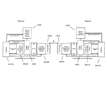
the "perturbed Q" and may be denoted by Qom as illustrated in Fig 4. In
general, there may be
many extraneous objects, denoted asp], p2, etc., or a set of extraneous
objects {pi, that perturb
the Q of the resonator 102. In this case, the perturbed Q may be denoted QW 4-
p2+..) or Qffp)). For
example, 00,aq-wood) may denote the perturbed quality factor 6f a first
resonator in a system for
wireless power exchange in the presence of a brick and a piece of wood, and
.Q2aõfficep may
CA 3011548 2018-07-17
= WO 2010/036980
PCT/US2009/058499 =
18
denote the perturbed quality factor of a second resonator in a system for
wireless power
exchange in an office environment.
100921 In some of the discussion herein, we define the "perturbing
quality factor" or
the "perturbing Q" due to an extraneous object, p, as 5Q 0,) , where 1/8Q0,)
W) . As
stated before, the perturbing quality factor may be due to multiple extraneous
objects, pl , p2, etc.
or a set of extraneous objects, (pl. The larger the perturbing Q, (5Q6,h of an
object, the less the
perturbed Q, Q6,), deviates from the unperturbed Q of the resonator.
[00931 In some of the discussion herein, we also define Ow Q()/ Q and.
call it the
"quality factor insensitivity" or the "Q-insensitivity" of the resonator in
the presence of an
extraneous object. A subscript index, such as 01(p) , indicates the resonator
to which the
perturbed and unperturbed quality factors are referring, namely, 0,(p) Q /Q1.
[00941 Note that the quality factor, Q, may also be characterized as
"unperturbed",
when necessary to distinguish it from the perturbed quality factor, Q6,), and
"unloaded", when
necessary to distinguish it from the loaded quality factor, Qty. Similarly,
the perturbed quality
factor, Q6,), may also be characterized as "unloaded", when necessary to
distinguish them from
the loaded perturbed quality factor, Qoxii.
[00951 Coupled Resonators
[0096] Resonators having substantially the same resonant frequency,
coupled through
any portion of their near-fields may interact and exchange energy. There are a
variety of physical
pictures and models that may be employed to understand, design, optimize and
characterize this
energy exchange. One way to describe and model the energy exchange between two
coupled
resonators is using coupled mode theory (CMT).
[00971 In coupled mode theory, the resonator fields obey the following
set of linear
equations:
da,(1) = i(com ¨ ir ) am(t)
dt ntin
where the indices denote different resonators and and rõ,õ are the coupling
coefficients between
the resonators. For a reciprocal system, the coupling coefficients may obey
the relation K.. = Kõ,,
Note that, for the purposes of the present specification, far-field radiation
interference effects
CA 3011548 2018-07-17
1111 WO 2010/036980
19
PCT/US2009/058499 411/
will be ignored and thus the coupling coefficients will be considered real.
Furthermore, since in
all subsequent calculations of system performance in this specification the
coupling coefficients
appear only with their square, K2 , we use Kõ,õ to denote the absolute value
of the real coupling
coefficients.
[0098] Note that the coupling coefficient, cõ, from the CMT described
above is
related to the so-called coupling factor, kõ,õ, between resonators in and n by
k,õ1---2r I c.11-7õcon .
We define a "strong-coupling factor", U , as the ratio of the coupling and
loss rates between
resonators m and n, by U,õõ = K,Jjrõyõ .
[00991 The quality factor of a resonator in, in the presence of a
similar frequency
resonator n or additional resonators, may be loaded by that resonator n or
additional resonators,
in a fashion similar to the resonator being loaded by a connected power
generating or consuming
device. The fact that resonator M may be loaded by resonator n and vice versa
is simply a
different way to see that the resonators are coupled.
[00100] The loaded Q's of the resonators in these cases may be denoted as QõN
and
For multiple resonators or loading supplies or devices, the total loading of a
resonator may
be determined by modeling each load as a resistive loss, and adding the
multiple loads in the
appropriate parallel and/or series combination to determine the equivalent
load of the ensemble.
[00101] In some of the discussion herein, we define the "loading quality
factor" or the
"loading Qõ," of resonator in due to resonator n as gQõ,(õJ , where 1/8Q,õ[)
Note
that resonator n is also loaded by resonator in and its "loading Qn" is given
by
1/d5Qõ[m] Va[mi -
[00102] When one or more of the resonators are connected to power generators
or
loads, the set of linear equations is modified to:
darn(t)
_____ = -i(com -Vrn ),õ,(0+i z xmnan(t) ¨tcmam(1)+ (t)
dt
s_m(0 = ,Px-mam(r)¨ s+m(1)
where s4 ,,(t) and s,(t) are respectively the amplitudes of the fields coming
from a generator into
the resonator in and going out of the resonator In either back towards the
generator or into a load,
õ1 õ1
defined so that the power they carry is given by s+, (t)12 and V)12 . The
loading coefficients
CA 3011548 2018-07-17
WO 2010/036980 20 PCT/1352009/058499
K. relate to the rate at which energy is exchanged between the resonator in
and the generator or
load connected to it.
[00103] Note that the loading coefficient, ./Cm , from the CMT described above
is
related to the loading quality factor, SQõiril , defined earlier, by 5Qõ41] =
c4,j2K,õ .
[00104] We define a "strong-loading factor", U.(,/, as the ratio of the
loading and loss
rates of resonator m, Umpl = Km /Fm =
[00105] Fig. 1(a) shows an example of two coupled resonators 1000, a first
resonator
102S, configured as a source resonator and a second resonator 102D, configured
as a device
resonator. Energy may be transferred over a distance D between the resonators.
The source
resonator 102S may be driven by a power supply or generator (not shown). Work
may be
extracted from the device resonator 102D by a power consuming drain or load
(e.g. a load
resistor, not shown). Let us use the subscripts "s" for the source, "d" for
the device, "g" for the
generator, and "1" for the load, and, since in this example there are only two
resonators and
== Ka=lcdõ let us drop the indices on led, Itsd, and Usd, and denote them
as K, k, and U, respectively.
[00106] The power generator may be constantly driving the source resonator at
a
constant driving frequency, f, corresponding to an angular driving frequency,
a), where co= 27rf.
[00107] In this case, the efficiency, =is-a12/1s2 of the power transmission
from
the generator to the load (via the source and device resonators) is maximized
under the following
conditions: The source resonant frequency, the device resonant frequency and
the generator
driving frequency have to be matched, namely
= = co -
Furthermore, the loading Q of the source resonator due to the generator,
SQ,Egi, has to be
matched (equal) to the loaded Q of the source resonator due to the device
resonator and the load,
Q3E43, and inversely the loading Q of the device resonator due to the load,
5Q4,1, has to be
matched (equal) to the loaded Q of the device resonator due to the source
resonator and the
generator, Qisgjnamely
(5Ufg] = Qs[dij and 8Qapi = Qd[sg] '
CA 3011548 2018-07-17
=
= WO
2010/036980 PCT/1JS2.009/058499 10
21
These equations determine the optimal loading rates of the source resonator by
the generator and
of the device resonator by the load as
Uatii = Ka ra .41+ U2 41+ (KAV¨rd )2 = iga[gi = Ks irs
Note that the above frequency matching and Q matching conditions are together
known as
"impedance matching" in electrical engineering.
[001081 Under the above conditions, the maximized efficiency is a
monotonically
increasing function of only the strong-coupling factor, U= = k4Q,Q,,
, between the source
and device resonators and is given by; 77 =-U21(1+ 1-1i7i112 , as shown in
Fig. 5. Note that the
coupling efficiency, 71, is greater than 1% when U is greater than 0.2, is
greater than 10% when
U is greater than 0.7, is greater than 17% when U is greater than 1, is
greater than 52% when U is
greater than 3, is greater than 80% when U is greater than 9, is greater than
90% when U is
greater than 19, and is greater than 95% when U is greater than 45. In some
applications, the
regime of operation where U>/ may be referred to as the "strong-coupling"
regime.
[001091 Since a large u= = (2K/ et.FaTT).XE is desired in certain
circumstances, resonators may be used that are high-Q. The Q of each resonator
may be high.
The geometric mean of the resonator Q's, 16E, may also or instead be high.
[00110] The coupling factor, k, is a number between 0:c1c5_1, and it may be
independent (or nearly independent) of the resonant frequencies of the source
and device
resonators, rather it may determined mostly by their relative geometry and the
physical decay-
law of the field mediating their coupling. In contrast, the coupling
coefficient, K-----kAwd
may be a strong function of the resonant frequencies. The resonant frequencies
of the resonators
may be chosen preferably to achieve a high Q rather than to achieve a low .r,
as these two goals
may be achievable at two separate resonant frequency regimes.
[00111] A high-Q resonator may be defined as one with Q>100. Two coupled
resonators may be referred to as a system of high-Q resonators when each
resonator has a Q
greater than 100, Qs>100 and Qd>100. In other implementationss, two coupled
resonators may be
referred to as a system of high-Q resonators when the geometric mean of the
resonator Q 's is
greater than 100, 4-0-:6; >100.
CA 3011548 2018-07-17
= e WO 2010/036980
PCT/11S2009/058499
22
[001121 The resonators may be named or numbered. They may be referred to as
source
resonators, device resonators, first resonators, second resonators, repeater
resonators, and the
like. It is to be understood that while two resonators are shown in Fig. 1,
and in many of the
examples below, other implementations may include three (3) or more
resonators. For example, a
single source resonator 102S may transfer energy to multiple device resonators
102D or multiple
devices. Energy may be transferred from a first device to a second, and then
from the second
device to the third, and so forth. Multiple sources may transfer energy to a
single device or to
multiple devices connected to a single device resonator or to multiple devices
connected to
multiple device resonators. Resonators 102 may serve alternately or
simultaneously as sources,
devices, or they may be used to relay power from a source in one location to a
device in another
location. Intermediate electromagnetic resonators 102 may be used to extend
the distance range
of wireless energy transfer systems. Multiple resonators 102 may be daisy
chained together,
exchanging energy over extended distances and with a wide range of sources and
devices. High
power levels may be split between multiple sources 102S, transferred to
multiple devices and
recombined at a distant location.
[00113] The analysis of a single source and a single device resonator may be
extended
to multiple source resonators and/or multiple device resonators and/or
multiple intermediate
resonators. In such an analysis, the conclusion may be that large strong-
coupling factors,
between at least some or all of the multiple resonators is preferred for a
high system efficiency in
the wireless energy transfer. Again, implementations may use source, device
and intermediate
resonators that have a high Q. The Q of each resonator may be high. The
geometric mean
of the Q's for pairs of resonators in and n, for which a large U is desired,
may also or instead
be high.
[00114] Note that since the strong-coupling factor of two resonators may be
determined by the relative magnitudes of the loss mechanisms of each resonator
and the coupling
mechanism between the two resonators, the strength of any or all of these
mechanisms may be
perturbed in the presence of extraneous objects in the vicinity of the
resonators as described
above.
[00115) Continuing the conventions for labeling from the previous sections, we
describe k as the coupling factor in the absence of extraneous objects or
materials. We denote the
CA 3011548 2018-07-17
= WO 2010/036980 PCT/IIS2009/058499 IP
23
coupling factor in the presence of an extraneous object, p, as kw, and call it
the "perturbed
coupling factor" or the "perturbed k". Note that the coupling factor, k, may
also be characterized
as "unperturbed", when necessary to distinguish from the perturbed coupling
factor Ic-64.
[00116] We define 61((,,y-T--kw-k and we call it the "perturbatiowon the
coupling factor"
or the "perturbation on k" due to an extraneous object, p.
[00117] We also define fia,)---1/(p)/k and we call it the "coupling factor
insensitivity" or
the "k-insensitivity". Lower indices, such as fii20), indicate the resonators
to which the perturbed
and unperturbed coupling factor is referred to, namelyfii49.E.-1/260c/2-
[00118] Similarly, we describe U as the strong-coupling factor in the absence
of
extraneous objects. We denote the strong-coupling factor in the presence of an
extraneous object,
p, as U60, 1.10,y= k(,)4Q,(p)Q2(,) , and call it the "perturbed strong-
coupling factor" or the
"perturbed U". Note that the strong-coupling factor Umay also be characterized
as
"unperturbed", when necessary to distinguish from the perturbed strong-
coupling factor U0,.).
Note that the strong-coupling factor Umay also be characterized as
"unperturbed", when
necessary to distinguish from the perturbed strong-coupling factor 144.
[00119] We define oU67)---U0,)-LT and call it the "perturbation on the strong-
coupling.
factor" or the "perturbation on U" due to an extraneous object, p.
[00120] We also define ,E(p)U6,./t/ and call it the "strong-coupling factor
insensitivity"
or the "U-insensitivity ". Lower indices, such as Ei2(,), indicate the
resonators to which the
perturbed and unperturbed coupling factor refers, namely E120,)---U1.20,1U12.
[00121] The efficiency of the energy exchange in a perturbed system may be
given by
the same formula giving the efficiency of the unperturbed system, where all
parameters such as
strong-coupling factors, coupling factors, and quality factors arc replaced by
their perturbed
equivalents. For example, in a system of wireless energy transfer including
one source and one
_________________________________________________________ -2 .
device resonator, the optimal efficiency may calculated as ri(p) =[U0,1(.1+
j1+U(,)2)
Therefore, in ,a system of wireless energy exchange which is perturbed by
extraneous objects,
large perturbed strong-coupling factors, between at least some or all of
the multiple
resonators may be desired for a high system efficiency in the wireless energy
transfer. Source,
device and/or intermediate resonators may have a high Q.
.
CA 3 0115 4 8 2 018 -0 7 -17
= WO 2010/036980
PCMS2009/058499 1111
24
[00122] Some extraneous perturbations may sometimes be detrimental for the
perturbed strong-coupling factors (via large perturbations on the coupling
factors or the quality
factors). Therefore, techniques may be used to reduce the effect of extraneous
perturbations on
the system and preserve large strong-coupling factor insensitivites.
[00123] Efficiency of Energy Exchange
[001241 The so-called "useful" energy in a useful energy exchange is the
energy or
power that must be delivered to a device (or devices) in order to power or
charge the device. The
transfer efficiency that corresponds to a useful energy exchange may be system
or application
dependent. For example, high power vehicle charging applications that transfer
kilowatts of
power may need to be at least 80% efficient in order to supply useful amounts
of power resulting
in a useful energy exchange sufficient to recharge a vehicle battery, without
significantly heating
up various components of the transfer system. In some consumer electronics
applications, a
useful energy exchange may include any energy transfer efficiencies greater
than 10%, or any
other amount acceptable to keep rechargeable batteries "topped off" and
running for long periods
of time. For some wireless sensor applications, transfer efficiencies that are
much less than 1%
may be adequate for powering multiple low power sensors from a single source
located a
significant distance from the sensors. For still other applications, where
wired power transfer is
either impossible or impractical, a wide range of transfer efficiencies may be
acceptable for a
useful energy exchange and may be said to supply useful power to devices in
those applications.
In general, an operating distance is any distance over which a useful energy
exchange is or can
be maintained according to the principles disclosed herein.
[00125] A useful energy exchange for a wireless energy transfer in a powering
or
recharging application may be efficient, highly efficient, or efficient
enough, as long as the
wasted energy levels, heat dissipation, and associated field strengths are
within tolerable limits.
The tolerable limits may depend on the application, the environment and the
system location.
Wireless energy transfer for powering or recharging applications may be
efficient, highly
efficient, or efficient enough, as long as the desired system performance may
be attained for the
reasonable cost restrictions, weight restrictions, size restrictions, and the
like. Efficient energy
transfer may be determined relative to that which could be achieved using
traditional inductive
techniques that are not high-Q systems. Then, the energy transfer may be
defined as being
efficient, highly efficient, or efficient enough, if more energy is delivered
than could be delivered
CA 3011548 2018-07-17
= WO 2010/036980 PCT/US2009/058499 illt
by similarly sized coil structures in traditional inductive schemes over
similar distances or
alignment offsets.
[00126] Note that, even though certain frequency and Q matching conditions may
optimize the system efficiency of energy transfer, these conditions may not
need to be exactly
met in order to have efficient enough energy transfer for a useful energy
exchange. Efficient
energy exchange may be realized so long as the relative offset of the resonant
frequencies
(I w ¨ is less than approximately the maximum among I/Q,õ(r), 1/Qõ(,)
and kõ,õ6,).
The Q matching condition may be less critical than the frequency matching
condition for
efficient energy exchange. The degree by which the strong-loading factors,
U41, of the
resonators due to generators and/or loads may be away from their optimal
values and still have
efficient enough energy exchange depends on the particular system, whether all
or some of the
generators and/or loads are Q-mismatched and so on.
[00127] Therefore, the resonant frequencies of the resonators may not be
exactly
matched, but may be matched within the above tolerances. The strong-loading
factors of at least
some of the resonators due to generators and/or loads may not be exactly
matched to their
optimal value. The voltage levels, current levels, impedance values, material
parameters, and the
like may not be at the exact values described in the disclosure but will be
within some acceptable
tolerance of those values. The system optimization may include cost, size,
weight, complexity,
and the like, considerations, in addition to efficiency, Q, frequency, strong
coupling factor, and
the like, considerations. Some system performance parameters, specifications,
and designs may
be far from optimal in order to optimize other system performance parameters,
specifications and
designs.
[00128] In some applications, at least some of the system parameters may be
varying
in time, for example because components, such as sources or devices, may be
mobile or aging or
because the loads may be variable or because the perturbations or the
environmental conditions
are changing etc. In these cases, in order to achieve acceptable matching
conditions, at least
some of the system parameters may need to be dynamically adjustable or
tunable. All the system
parameters may be dynamically adjustable or tunable to achieve approximately
the optimal
operating conditions. However, based on the discussion above, efficient enough
energy exchange
may be realized even if some system parameters are not variable. In some
examples, at least
=
CA 3011548 2018-07-17
= WO 2010/036980 26
PCT/US2009/058499 =
some of the devices may not be dynamically adjusted. In some examples, at
least some of the
sources may not be dynamically adjusted. In some examples, at least some of
the intermediate
resonators may not be dynamically adjusted. In some examples, none of the
system parameters
may be dynamically adjusted.
[00129] Electromagnetic Resonators
[00130] The resonators used to exchange energy may be electromagnetic
resonators.
In such resonators, the intrinsic energy decay rates, rm, are given by the
absorption (or resistive)
losses and the radiation losses of the resonator.
[00131] The resonator may be constructed such that the energy stored by the
electric
field is primarily confined within the structure and that the energy stored by
the magnetic field is
primarily in the region surrounding the resonator. Then, the energy exchange
is mediated
primarily by the resonant magnetic near-field. These types of resonators may
be referred to as
magnetic resonators.
[00132] The resonator may be constructed such that the energy stored by the
magnetic
field is primarily confined within the structure and that the energy stored by
the electric field is
primarily in the region surrounding the resonator. Then, the energy exchange
is mediated
primarily by the resonant electric near-field. These types of resonators may
be referred to as
electric resonators.
[00133] Note that the total electric and magnetic energies stored by the
resonator have
to be equal, but their localizations may be quite different. In some cases,
the ratio of the average
electric field energy to the average magnetic field energy specified at a
distance from a resonator
may be used to characterize or describe the resonator.
[00134] Electromagnetic resonators may include an inductive clement, a
distributed
inductance, or a combination of inductances with inductance, L, and a
capacitive element, a
distributed capacitance, or a combination of capacitances, with capacitance,
C. A minimal circuit
model of an electromagnetic resonator 102 is shown in Fig. 6a. The resonator
may include an
inductive element 108 and a capacitive element 104. Provided with initial
energy, such as
electric field energy stored in the capacitor 104, the system will oscillate
as thp capacitor
discharges transferring energy into magnetic field energy stored in the
inductor 108 which in turn
transfers energy back into electric field energy stored in the capacitor 104.
=
CA 3011548 2018-07-17
SI WO 2010/036980 PCT/US2009/058499
27
[00135] The resonators 102 shown in Figs. 6(b)(c)(d) may be referred to
as magnetic
resonators. Magnetic resonators may be preferred for wireless energy transfer
applications in
populated environments because most everyday materials including animals,
plants, and humans
are non-magnetic (i.e., p.,;-=--1), so their interaction with magnetic fields
is minimal and due
primarily to eddy currents induced by the time-variation of the magnetic
fields, which is a
second-order effect. This characteristic is important both for safety reasons
and because it
reduces the potential for interactions with extraneous environmental objects
and materials that
could alter system performance.
[00136] Fig. 6d shows a simplified drawing of some of the electric and
magnetic field
lines associated with an exemplary magnetic resonator 102B. The magnetic
resonator 102B may
include a loop of conductor acting as an inductive element 108 and a
capacitive element 104 at
the ends of the conductor loop. Note that this drawing depicts most of the
energy in the region
surrounding the resonator being stored in the magnetic field, and most of the
energy in the
resonator (between the capacitor plates) stored in the electric field. Some
electric field, owing to
fringing fields, free charges, and the time varying magnetic field, may be
stored in the region
around the resonator, but the magnetic resonator may be designed to confine
the electric fields to
be close to or within the resonator itself, as much as possible.
[00137] The inductor 108 and capacitor 104 of an electromagnetic resonator 102
may
be bulk circuit elements, or the inductance and capacitance may be distributed
and may result
from the way the conductors are formed, shaped, or positioned, in the
structure. For example, the
inductor 108 may be realized by shaping a conductor to enclose a surface area,
as shown in Figs.
6(b)(c)(d). This type of resonator 102 may be referred to as a capacitively-
loaded loop inductor.
Note that we may use the terms "loop" or "coil" to indicate generally a
conducting structure
(wire, tube, strip, etc.), enclosing a surface of any shape and dimension,
with any number of
turns. In Fig. 6b, the enclosed surface area is circular, but the surface may
be any of a wide
variety of other shapes and sizes and may be designed to achieve certain
system performance
specifications. As an example to indicate how inductance scales with physical
dimensions, the
inductance for a length of circular conductor arranged to form a circular
single-turn loop is
approximately,
8x
L pox(ln--- 2),
a
CA 3011548 2018-07-17
wo 2010/036980
PCT/1JS2009/058499 = =
28
where po is the magnetic permeability of free space, x, is the radius of the
enclosed circular
surface area and, a, is the radius of the conductor used to form the inductor
loop. A more precise
value of the inductance of the loop may be calculated analytically or
numerically.
[00138] The inductance for other cross-section conductors, arranged to form
other
enclosed surface shapes, areas, sizes, and the like, and of any number of wire
turns, may be
calculated analytically, numerically or it may be determined by measurement.
The inductance
may be realized using inductor elements, distributed inductance, networks,
arrays, series and
parallel combinations of inductors and inductances, and the like. The
inductance may be fixed or
variable and may be used to vary impedance matching as well as resonant
frequency operating
conditions.
[00139] There are a variety of ways to realize the capacitance required to
achieve the
desired resonant frequency for a resonator structure. Capacitor plates 110 may
be formed and
utilized as shown in Fig. 6b, or the capacitance may be distributed and be
realized between
adjacent windings of a multi-loop conductor 114, as shown in Fig. 6c. The
capacitance may be
realized using capacitor elements, distributed capacitance, networks, arrays,
series and parallel
combinations of capacitances, and the like. The capacitance may be fixed or
variable and may be
used to vary impedance matching as well as resonant frequency operating
conditions.
[001401 It is to be understood that the inductance and capacitance in an
electromagnetic resonator 102 may be lumped, distributed, or a combination of
lumped and
distributed inductance and capacitance and that electromagnetic resonators may
be realized by
combinations of the various elements, techniques and effects described herein.
[00141] Electromagnetic resonators 102 may be include inductors, inductances,
capacitors, capacitances, as well as additional circuit elements such as
resistors, diodes, switches,
amplifiers, diodes, transistors, transformers, conductors, connectors and the
like.
[00142] Resonant Frequency of an Electromagnetic Resonator
[00143] An electromagnetic resonator 102 may have a characteristic, natural,
or
resonant frequency determined by its physical properties. This resonant
frequency is the
frequency at which the energy stored by the resonator oscillates between that
stored by the
electric field, WE, (WE=q2/2C, where q is the charge on the capacitor, C) and
that stored by the
magnetic field, WB, (Wa.---Li2/2, where i is the current through the inductor,
L) of the resonator.
In the absence of any losses in the system, energy would continually be
exchanged between the
CA 3011548 2018-07-17
diW.2010/036980 29
PCT/US2009/058499 1111
electric field in the capacitor 104 and the magnetic field in the inductor
108. The frequency at
which this energy is exchanged may be called the characteristic frequency, the
natural frequency,
or the resonant frequency of the resonator, and is given by co,
=
co= 2.7r f = .
LC
[001441 The resonant frequency of the resonator may be changed by tuning the
inductance, L, and/or the capacitance, C, of the resonator. The resonator
frequency may be
design to operate at the so-called ISM (Industrial, Scientific and Medical)
frequencies as
specified by the FCC. The resonator frequency may be chosen to meet certain
field limit
specifications, specific absorption rate (SAR) limit specifications,
electromagnetic compatibility
(EMC) specifications, electromagnetic interference (EMI) specifications,
component size, cost or
performance specifications, and the like.
[001451 Quality Factor of an Electromagnetic Resonator
[001461 The energy in the resonators 102 shown in Fig. 6 may decay or be lost
by
intrinsic losses including absorptive losses (also called ohmic or resistive
losses) and/or radiative
losses. The Quality Factor, or Q, of the resonator, which characterizes the
energy decay, is
inversely proportional to these losses. Absorptive losses may be caused by the
finite conductivity
of the conductor used to form the inductor as well as by losses in other
elements, components,
connectors, and the like, in the resonator. An inductor formed from low loss
materials may be
referred to as a "high-Q inductive element" and elements, components,
connectors and the like
with low losses may be referred to as having "high resistive Q's". In general,
the total absorptive
loss for a resonator may be calculated as the appropriate series and/or
parallel combination of
resistive losses for the various elements and components that make up the
resonator. That is, in
the absence of any significant radiative or component/connection losses, the Q
of the resonator
may be given by, Qabs,
coL
Qabs = f
where co, is the resonant frequency, L, is the total inductance of the
resonator and the resistance
for the conductor used to form the inductor, for example, may be given by Raõ
the
length of the wire, p is the resistivity of the conductor material, and A is
the cross-sectional area
over which current flows in the wire). For alternating currents, the cross-
sectional area over
CA 3011548 2018-07-17
= WO 2010/036980
PCTMS2009/058499
which current flows may be less than the physical cross-sectional area of the
conductor owing to
the skin effect. Therefore, high-Q magnetic resonators may be composed of
conductors with high
conductivity, relatively large surface areas and/or with specially designed
profiles (e.g. Litz wire)
to minimize proximity effects and reduce the AC resistance.
[00147] The magnetic resonator structures may include high-Q inductive
elements
composed of high conductivity wire, coated wire, Litz wire, ribbon, strapping
or plates, tubing,
paint, gets, traces, and the like. The magnetic resonators may be self-
resonant or they may
include external coupled elements such as capacitors, inductors, switches,
diodes, transistors,
transformers, and the like. The magnetic resonators may include distributed
and lumped
capacitance and inductance. In general, the Q of the resonators will be
determined by the Q's of
all the individual components of the resonator.
[00148] Because Q is proportional to inductance, L, resonators may be designed
to
increase L, within certain other constraints. One way to increase L, for
example, is to use more
than one turn of the conductor to form the inductor in the resonator. Design
techniques and trade-
offs may depend on the application, and a wide variety of structures,
conductors, components,
and resonant frequencies may be chosen in the design of high-Q magnetic
resonators.
[00149] In the absence of significant absorption losses, the Q of the
resonator may be
determined primarily by the radiation losses, and given by, Q, = wL/R, ,where
Rrad is the
radiative loss of the resonator and may depend on the size of the resonator
relative to the
frequency, co, or wavelength, 2, of operation. For the magnetic resonators
discussed above,
radiative losses may scale as 1?, ,,d (x/ A)4 (characteristic of magnetic
dipole radiation), where x
is a characteristic dimension of the resonator, such as the radius of the
inductive element shown
in Fig. 6b, and whereyi = c I f , where c is the speed of light and f is as
defined above. The size
of the magnetic resonator may be much less than the wavelength of operation so
radiation losses
may be very small. Such structures may be referred to as sub-wavelength
resonators. Radiation
may be a loss mechanism for non-radiative wireless energy transfer systems and
designs may be
chosen to reduce or minimize Rrad. Note that a high-Qrad may be desirable for
non-radiative
wireless energy transfer schemes.
[00150] Note too that the design of resonators for non-radiative wireless
energy
transfer differs from antennas designed for communication or far-field energy
transmission
CA 3011548 2018-07-17
= WO 2010/036980
PCT/US2009/058499
31
purposes. Specifically, capacitively-loaded conductive loops may be used as
resonant antennas
(for example in cell phones), but those operate in the far-field regime where
the radiation Q's are
intentionally designed to be small to make the antenna efficient at radiating
energy. Such designs
are not appropriate for the efficient near-field wireless energy transfer
technique disclosed in this
application.
[00151] The quality factor of a resonator including both radiative and
absorption
losses is Q. coLARth, +1?). Note that there may be a maximum Q value for a
particular
resonator and that resonators may be designed with special consideration given
to the size of the
resonator, the materials and elements used to construct the resonator, the
operating frequency,
the connection mechanisms, and the like, in order to achieve a high-Q
resonator. Fig. 7 shows a
plot of Q of an exemplary magnetic resonator (in this case a coil with a
diameter of 60 cm made
of copper pipe with an outside diameter (OD) of 4 cm) that may be used for
wireless power
transmission at MHz frequencies. The absorptive Q (dashed line) 702 increases
with frequency,
while the radiative Q (dotted line) 704 decreases with frequency, thus leading
the overall Q to
peak 708 at a particular frequency. Note that the Q of this exemplary
resonator is greater than
100 over a wide frequency range. Magnetic resonators may be designed to have
high-Q over a
range of frequencies and system operating frequency may set to any frequency
in that range.
[00152] When the resonator is being described in terms of loss rates, the Q
may be
defined using the intrinsic decay rate, 2T, as described previously. The
intrinsic decay rate is the
rate at which an uncoupled and undriven resonator loses energy. For the
magnetic resonators
described above, the intrinsic loss rate may be given by F =(R, +R,)/2L, and
the quality
factor, Q, of the resonator is given by Q= 42F.
[00153] Note that a quality factor related only to a specific loss mechanism
may be
denoted as Qõ,,hani.,õõ if the resonator is not specified, or as 0
1, mechanism) if the resonator is
specified (e.g. resonator 1). For example, 0
,r.,I,rad is the quality factor for resonator 1 related to its
radiation losses.
[00154] Electromagnetic Resonator Near-Fields
[00155) The high-Q electromagnetic resonators used in the near-field wireless
energy
transfer system disclosed here may be sub-wavelength objects. That is, the
physical dimensions
of the resonator may be much smaller than the wavelength corresponding to the
resonant
CA 3011548 2018-07-17
410 WO 2010/036980 32
PCT/US2009/058499 =
frequency. Sub-wavelength magnetic resonators may have most of the energy in
the region
surrounding the resonator stored in their magnetic near-fields, and these
fields may also be
described as stationary or non-propagating because they do not radiate away
from the resonator.
The extent of the near-field in the area surrounding the resonator is
typically set by the
wavelength, so it may extend well beyond the resonator itself for a sub-
wavelength resonator.
The limiting surface, where the field behavior changes from near-field
behavior to far-field
behavior may be called the "radiation caustic".
[00156] The strength of the near-field is reduced the farther one gets away
from the
resonator. While the field strength of the resonator near-fields decays away
from the resonator,
the fields may still interact with objects brought into the general vicinity
of the resonator. The
degree to which the fields interact depends on a variety of factors, some of
which may be
controlled and designed, and some of which may not. The wireless energy
transfer schemes
described herein may be realized when the distance between coupled resonators
is such that one
resonator lies within the radiation caustic of the other.
[00157] The near-field profiles of the electromagnetic resonators may be
similar to
those commonly associated with dipole resonators or oscillators. Such field
profiles may be
described as ornni-directional, meaning the magnitudes of the fields are non-
zero in all directions
away from the object.
[00158] Characteristic Size of An Electromagnetic Resonator
[00159] Spatially separated and/or offset magnetic resonators of sufficient Q
may
achieve efficient wireless energy transfer over distances that are much larger
than have been seen
in the prior art, even if the sizes and shapes of the resonator structures are
different. Such
resonators may also be operated to achieve more efficient energy transfer than
was achievable
with previous techniques over shorter range distances. We describe such
resonators as being
capable of mid-range energy transfer.
1001601 Mid-range distances may be defined as distances that are larger than
the
characteristic dimension of the smallest of the resonators involved in the
transfer, where the
distance is measured from the center of one resonator structure to the center
of a spatially
separated second resonator structure. In this definition, two-dimensional
resonators are spatially
separated when the areas circumscribed by their inductive elements do not
intersect and three-
dimensional resonators are spatially separated when their volumes do not
intersect. A two-
CA 3011548 2018-07-17
41 WO 2010/036980 PCT/US2009/058499
33
dimensional resonator is spatially separated from a three-dimensional
resonator when the area
circumscribed by the former is outside the volume of the latter.
[00161] Fig. 8 shows some example resonators with their characteristic
dimensions
labeled. It is to be understood that the characteristic sizes 802 of
resonators 102 may be defined
in terms of the size of the conductor and the area circumscribed or enclosed
by the inductive
element in a magnetic resonator and the length of the conductor forming the
capacitive element
of an electric resonator. Then, the characteristic size 802 of a resonator
102, xchar, may be equal
to the radius of the smallest sphere that can fit around the inductive or
capacitive element of the
magnetic or electric resonator respectively, and the center of the resonator
structure is the center
of the sphere. The characteristic thickness 804, tchar, of a resonator 102 may
be the smallest
possible height of the highest point of the inductive or capacitive element in
the magnetic or
capacitive resonator respectively, measured from a flat surface on which it is
placed. The
characteristic width 808 of a resonator 102, wdiar, may be the radius of the
smallest possible
circle through which the inductive or capacitive element of the magnetic or
electric resonator
respectively, may pass while traveling in a straight line. For example, the
characteristic width
808 of a cylindrical resonator may be the radius of the cylinder.
[00162] In this inventive wireless energy transfer technique, energy may be
exchanged
efficiently over a wide range of distances, but the technique is distinguished
by the ability to
exchange useful energy for powering or recharging devices over mid-range
distances and
between resonators'with different physical dimensions, components and
orientations. Note that
while k may be small in these circumstances, strong coupling and efficient
energy transfer may
be realized by using high-Q resonators to achieve a high U, U = k.µ1Q,Q, .
That is, increases in Q
may be used to at least partially overcome decreases in k, to maintain useful
energy transfer
efficiencies.
[001631 Note too that while the near-field of a single resonator may be
described as
omni-directional, the efficiency of the energy exchange between two resonators
may depend on
the relative position and orientation of the resonators. That is, the
efficiency of the energy
exchange may be maximized for particular relative orientations of the
resonators. The sensitivity
of the transfer efficiency to the relative position and orientation of two
uncompensated
resonators may be captured in the calculation of either k or K. While coupling
may be achieved
between resonators that are offset and/or rotated relative to each other, the
efficiency of the
CA 3011548 2018-07-17
= WO 2010/036980
PCT/US2009/058499 1111
34
exchange may depend on the details of the positioning and on any feedback,
tuning, and
compensation techniques implemented during operation.
[00164] High-0 Magnetic Resonators
[00165] In the near-field regime of a sub-wavelength capacitively-loaded loop
magnetic resonator (x 1), the resistances associated with a circular
conducting loop inductor
composed of N turns of wire whose radius is larger than the skin depth, are
approximately
= /v6)12 = Nx I a and /6. in1r2
(cox/ c)4, where p is the resistivity of the conductor
material and in 1207r n is the impedance of free space. . The inductance, L,
for such a N-turn
loop is approximately N2 times the inductance of a single-turn loop given
previously. The quality
factor of such a resonator, Q= coL I (R, , is
highest for a particular frequency determined
by the system parameters (Fig. 4). As described previously, at lower
frequencies the Q is
determined primarily by absorption losses and at higher frequencies the Q is
determined
primarily by radiation losses.
[00166] Note that the formulas given above are approximate and intended to
illustrate
the functional dependence of Robs) Rrad and L on the physical parameters of
the structure. More
accurate numerical calculations of these parameters that take into account
deviations from the
strict quasi-static limit, for example a non-uniform current/charge
distribution along the
conductor, may be useful for the precise design of a resonator structure.
[00167] Note that the absorptive losses may be minimized by using low loss
conductors to form the inductive elements. The loss of the conductors may be
minimized by
using large surface area conductors such as conductive tubing, strapping,
strips, machined
objects, plates, and the like, by using specially designed conductors such as
Litz wire, braided
wires, wires of any cross-section, and other conductors with low proximity
losses, in which case
the frequency scaled behavior described above may be different, and by using
tow resistivity
materials such as high-purity copper and silver, for example. One advantage of
using conductive
tubing as the conductor at higher operating frequencies is that it may be
cheaper and lighter than
a similar diameter solid conductor, and may have similar resistance because
most of the current
is traveling along the outer surface of the conductor owing to the skin
effect.
[00168] To get a rough estimate of achievable resonator designs made from
copper
wire or copper tubing and appropriate for operation in the microwave regime,
one may calculate
CA 3011548 2018-07-17
= WO 2010/036980
PCT/US2009/058499 =
the optimum Q and resonant frequency for a resonator composed of one circular
inductive
element (N=1) of copper wire (p=1.69-1(14 Qm) with various cross sections.
Then for an
inductive element with characteristic size x=1 cm and conductor diameter a=1
mm, appropriate
for a cell phone for example, the quality factor peaks at Q=1225 wherif=380
MHz. For x=30 cm
and a=2 mm, an inductive element size that might be appropriate for a laptop
or a household
robot, Q=1103 at f=17 MHz. For a larger source inductive element that might be
located in the
ceiling for example, x=1 m and a=4 mm, Q may be as high as Q=1315 at f=5 MHz.
Note that a
number of practical examples yield expected quality factors of Q----1000-1500
at )trz50-80.
Measurements of a wider variety of coil shapes, sizes, materials and operating
frequencies than
described above show that Q's >100 may be realized for a variety of magnetic
resonator
structures using commonly available materials.
[00169] As described above, the rate for energy transfer between two
resonators of
characteristic size xJ and x2, and separated by a distance D between their
centers, may be given
by ic . To give an example of how the defined parameters scale, consider the
cell phone, laptop,
and ceiling resonator examples from above, at three (3) distances; D/x=10, 8,
6. In the examples
considered here, the source and device resonators are the same size, xl=12,
and shape, and are
oriented as shown in Fig. 1(b). In the cell phone example, 0/ 2K =3033, 1553,
655 respectively.
In the laptop example, o.)/ 21c =7131, 3651, 1540 respectively and for the
ceiling resonator
example, col 2x- =6481, 3318, 1400. The corresponding coupling-to-loss ratios
peak at the
frequency where the inductive element Q pealcs and are I 1- =0.4, 0.79, 1.97
and 0.15, 0.3, 0.72
and 0.2, 0.4, 0.94 for the three inductive element sizes and distances
described above. An
example using different sized inductive elements is that of an xi=1 m inductor
(e.g. source in the
ceiling) and an x2=30 cm inductor (e.g. household robot on the floor) at a
distance D=3 m apart
(e.g. room height). In this example, the strong-coupling figure of merit, U
=tc-/ vr,r, =0.88, for
an efficiency of approximately 14%, at the optimal operating frequency off=6.4
MHz. Here, the
optimal system operating frequency lies between the peaks of the individual
resonator Q's.
[00170] Inductive elements may be formed for use in high-Q magnetic
resonators. We
have demonstrated a variety of high-Q magnetic resonators based on copper
conductors that are
formed into inductive elements that enclose a surface. Inductive elements may
be formed using a
variety of conductors arranged in a variety of shapes, enclosing any size or
shaped area, and they
may be single turn or multiple turn elements. Drawings of exemplary inductive
elements 900A-B
CA 3011548 2018-07-17
= WO 2010/036980
PCMIS2009/058499
36
are shown in Fig. 9. The inductive elements may be formed to enclose a circle,
a rectangle, a
square, a triangle, a shape with rounded corners, a shape that follows the
contour of a particular
structure or device, a shape that follows, fills, or utilizes, a dedicated
space within a structure or
device, and the like. The designs may be optimized for size, cost, weight,
appearance,
performance, and the like.
[00171] These conductors may be bent or formed into the desired size, shape,
and
number of turns. However, it may be difficult to accurately reproduce
conductor shapes and sizes
using manual techniques. In addition, it may be difficult to maintain uniform
or desired center-
to-center spacings between the conductor segments in adjacent turns of the
inductive elements.
Accurate or uniform spacing may be important in determining the self
capacitance of the
structure as well as any proximity effect induced increases in AC resistance,
for example.
[001721 Molds may be used to replicate inductor elements for high-Q resonator
designs. In addition, molds may be used to accurately shape conductors into
any kind of shape
without creating kinks, buckles or other potentially deleterious effects in
the conductor. Molds
may be used to form the inductor elements and then the inductor elements may
be removed from
the forms. Once removed, these inductive elements may be built into enclosures
or devices that
may house the high-Q magnetic resonator. The formed elements may also or
instead remain in
the mold used to form them.
[001731 The molds may be formed using standard CNC (computer numerical
control)
routing or milling tools or any other known techniques for cutting or forming
grooves in blocks.
The molds may also or instead be formed using machining techniques, injection
molding
techniques, casting techniques, pouring techniques, vacuum techniques,
thermoforming
techniques, cut-in-place techniques, compression forming techniques and the
like.
[00174] The formed element may be removed from the mold or it may remain in
the
mold. The mold may be altered with the inductive element inside. The mold may
be covered,
machined, attached, painted and the like. The mold and conductor combination
may be
integrated into another housing, structure or device. The grooves cut into the
molds may be any
dimension and may be designed to form conducting tubing, wire, strapping,
strips, blocks, and
the like into the desired inductor shapes and sizes.
[00175] The inductive elements used in magnetic resonators may contain more
than
one loop and may spiral inward or outward or up or down or in some combination
of directions.
CA 3011548 2018-07-17
=
WO 2010/036980 PCT/US2009/058499 =
37
In general, the magnetic resonators may have a variety of shapes, sizes and
number of turns and
they may be composed of a variety of conducing materials.
1001761 The magnetic resonators may be free standing or they may be enclosed
in an
enclosure, container, sleeve or housing. The magnetic resonators may include
the form used to
make the inductive element. These various forms and enclosures may be composed
of almost
any kind of material. Low loss materials such as Teflon, REXOLITE, styrene,
and the like may
be preferable for some applications. These enclosures may contain fixtures
that hold the
inductive elements.
[001771 Magnetic resonators may be composed of self-resonant coils of copper
wire or
copper tubing. Magnetic resonators composed of self resonant conductive wire
coils may include
a wire of length 1, and cross section radius a, wound into a helical coil of
radius x, height h, and
number of turns N, which may for example be characterized as N = NI12 -71-72 1
22rx
[001781 A magnetic resonator structure may be configured so that x is about 30
cm, h
is about 20 cm, a is about 3 mm and N is about 5.25, and, during operation, a
power source
coupled to the magnetic resonator may drive the resonator at a resonant
frequency, f, where f is
about 10.6 MHz. Where x is about 30 cm, h is about 20 cm, a is about 1 cm and
Nis about 4, the
resonator may be driven at a frequency, f, where f is about 13.4 MHz. Where x
is about 10 cm, h
is about 3 cm, a is about 2 mm and N is about 6, the resonator may be driven
at a frequency, f,
where f is about 21.4 MHz.
[00179] High-Q inductive elements may be designed using printed circuit board
traces.
Printed circuit board traces may have a variety of advantages compared to
mechanically formed
inductive elements including that they may be accurately reproduced and easily
integrated using
established printed circuit board fabrication techniques, that their AC
resistance may be lowered
using custom designed conductor traces, and that the cost of mass-producing
them may be
significantly reduced.
[00180] High-Q inductive elements may be fabricated using standard PCB
techniques
on any PCB material such as FR-4 (epoxy E-glass), multi-functional epoxy, high
performance
epoxy, bismalaimide triazine/epoxy, polyimide, Cyanatc Ester,
polytetraflouroethylene (Teflon),
FR-2, FR-3, CEM-1, CEM-2, Rogers, Resolute, and the like. The conductor traces
may be
formed on printed circuit board materials with lower loss tangents.
CA 3011548 2018-07-17
111 w0 2010/036980
PCT/US2009/058499 =
38
[00181] The conducting traces may be composed of copper, silver, gold,
aluminum,
nickel and the like, and they may be composed of paints, inks, or other cured
materials. The
circuit board may be flexible and it may be a flex-circuit. The conducting
traces may be formed
by chemical deposition, etching, lithography, spray deposition, cutting, and
the like. The
conducting traces may be applied to form the desired patterns and they may be
formed using
crystal and structure growth techniques.
[00182] The dimensions of the conducting traces, as well as the number of
layers
containing conducting traces, the position, size and shape of those traces and
the architecture for
interconnecting them may be designed to achieve or optimize certain system
specifications such
as resonator Q, gp), resonator size, resonator material and fabrication costs,
U, Uo, and the like.
[00183] As an example, a three-turn high-Q inductive element 1001A was
fabricated
on a four-layer printed circuit board using the rectangular copper trace
pattern as shown in Fig.
10(a). The copper trace is shown in black and the PCB in white. The width and
thickness of the
copper traces in this example was approximately 1 cm (400 mils) and 43 # m
(1.7 mils)
respectively. The edge-to-edge spacing between turns of the conducting trace
on a single layer
was approximately 0.75 cm (300 mils) and each board layer thickness was
approximately 100 g
m (4 mils). The pattern shown in Fig. 10(a) was repeated on each layer of the
board and the
conductors were connected in parallel. The outer dimensions of the 3-loop
structure were -
approximately 30 cm by 20 cm. The measured inductance of this PCB loop was 5.3
p 11. A
magnetic resonator using this inductor element and tunable capacitors had a
quality factor, Q, of
550 at its designed resonance frequency of 6.78 MHz. The resonant frequency
could be tuned by
changing the inductance and capacitance values in the magnetic resonator.
[001841 As another example, a two-turn inductor 1001B was fabricated on a four-
layer
printed circuit board using the rectangular copper trace pattern shown in Fig.
10(b). The copper
trace is shown in black and the PCB in white. The width and height of the
copper traces in this
example were approximately 0.75 cm (300 mils) and 43 g m (1.7 mils)
respectively. The edge-
to-edge spacing between turns of the conducting trace on a single layer was
approximately 0.635
cm (250 mils) and each board layer thickness was approximately 100 m (4 mils).
The pattern
shown in Fig. 10(b) was repeated on each layer of the board and the conductors
were connected
in parallel. The outer dimensions of the two-loop structure were approximately
7.62 cm by 26.7
CA 3011548 2018-07-17
111, WO 2010/036980
PCIMS2009/058499 =
39
cm. The measured inductance of this PCB loop was 1.3 p H. Stacking two boards
together with
a vertical separation of approximately 0.635 cm (250 mils) and connecting the
two boards in
series produced a PCB inductor with an inductance of approximately 3.4 p H. A
magnetic
resonator using this stacked inductor loop and tunable capacitors had a
quality factor, Q, of 390
at its designed resonance frequency of 6.78 MHz. The resonant frequency could
be tuned by
changing the inductance and capacitance values in.the magnetic resonator.
[00185] The inductive elements may be formed using magnetic materials of any
size,
shape thickness, and the like, and of materials with a wide range of
permeability and loss values.
These magnetic materials may be solid blocks, they may enclose hollow volumes,
they may be
formed from many smaller pieces of magnetic material tiled and or stacked
together, and they
may be integrated with conducting sheets or enclosures made from highly
conducting materials.
Wires may be wrapped around the magnetic materials to generate the magnetic
near-field. These
wires may be wrapped around one or more than one axis of the structure.
Multiple wires may be
wrapped around the magnetic materials and combined in parallel, or in series,
or via a switch to
form customized near-field patterns.
[00186] The magnetic resonator may include 15 turns of Litz wire wound around
a
19.2 cm x 10 cm x 5 mm tiled block of 3F3 ferrite material. The Litz wire may
be wound around
the ferrite material in any direction or combination of directions to achieve
the desire resonator
performance. The number of turns of wire, the spacing between the turns, the
type of wire, the
size and shape of the magnetic materials and the type of magnetic material are
all design
parameters that may be varied or optimized for different application
scenarios.
[00187] 1-ligh-Q Magnetic resonators using magnetic material structures
[00188] It may be possible to use magnetic materials assembled to form an open
magnetic circuit, albeit one with an air gap on the order of the size of the
whole structure, to
realize a magnetic resonator structure. In these structures, high conductivity
materials are wound
around a structure made from magnetic material to form the inductive element
of the magnetic
resonator. Capacitive elements may be connected to the high conductivity
materials, with the
resonant frequency then determined as described above. These magnetic
resonators have their
dipole moment in the plane of the two dimensional resonator structures, rather
than
perpendicular to it, as is the case for the capacitively-loaded inductor loop
resonators.
CA 3011548 2018-07-17
= WO
20101036980 PC1/US2009/058499 IP
[00189) A diagram of a single planar resonator structure is shown in Fig.
11(a). The
planar resonator structure is constructed of a core of magnetic material 1121,
such as ferrite with
a loop or loops of conducting material 1122 wrapped around the core 1121. The
structure may be
used as the source resonator that transfers power and the device resonator
that captures energy.
When used as a source, the ends of the conductor may be coupled to a power
source. Alternating
electrical current flowing through the conductor loops excites alternating
magnetic fields. When
the structure is being used to receive power, the ends of the conductor may be
coupled to a
power drain or load. Changing magnetic fields induce an electromotive force in
the loop or loops
of the conductor wound around the core magnetic material. The dipole moment of
these types of
structures is in the plane of the structures and is, for example, directed
along the Y axis for the
structure in Figure 11(a). Two such structures have strong coupling when
placed substantially in
the same plane (i.e. the X,Y plane of Figure 11). The structures of Figure
11(a) have the most
favorable orientation when the resonators are aligned in the same plane along
their Y axis.
[00190] The geometry and the coupling orientations of the described planar
resonators
may be preferable for some applications. The planar or flat resonator shape
may be easier to
integrate into many electronic devices that are relatively flat and planar.
The planar resonators
may be integrated into the whole back or side of a device without requiring a
change in geometry
of the device. Due to the flat shape of many devices, the natural position of
the devices when
placed on a surface is to lay with their largest dimension being parallel to
the surface they are
placed on. A planar resonator integrated into a flat device is naturally
parallel to the plane of the
surface and is in a favorable coupling orientation relative to the resonators
of other devices or
planar resonator sources placed on a flat surface.
[00191] As mentioned, the geometry of the planar resonators may allow easier
integration into devices. Their low profile may allow a resonator to be
integrated into or as part
of a complete side of a device. When a whole side of a device is covered by
the resonator,
magnetic flux can flow through the resonator core without being obstructed by
lossy material
that may be part of the device or device circuitry.
[00192] The core of the planar resonator structure may be of a variety of
shapes and
thicknesses and may be flat or planar such that the minimum dimension does not
exceed 30% of
the largest dimension of the structure. The core may have complex geometries
and may have
indentations, notches, ridges, and the like. Geometric enhancements may be
used to reduce the
CA 3011548 2018-07-17
= WO 2010/036980
PCT/US2009/058499 IP.
41
coupling dependence on orientation and they may be used to facilitate
integration into devices,
packaging, packages, enclosures, covers, skins, and the like. Two exemplary
variations of core
geometries are shown in Figure 11(b). For example, the planar core 1131 may be
shaped such
that the ends are substantially wider than the middle of the structure to
create an indentation for
the conductor winding. The core material may be of varying thickness with ends
that are thicker
and wider than the middle. The core material 1132 may have any number of
notches or cutouts
1133 of various depths, width, and shapes to accommodate conductor loops,
housing, packaging,
and the like.
[00193] The shape and dimensions of the core may be further dictated by the
dimensions and characteristics of the device that they are integrated into.
The core material may
curve to follow the contours of the device, or may require non-symmetric
notches or cutouts to
allow clearance for parts of the device. The core structure may be a single
monolithic piece of
magnetic material or may be composed of a plurality of tiles, blocks, or
pieces that are arranged
together to form the larger structure. The different layers, tiles, blocks, or
pieces of the structure
may be of similar or may be of different materials. It may be desirable to use
materials with
different magnetic permeability in different locations of the structure. Core
structures with
different magnetic permeability may be useful for guiding the magnetic flux,
improving
coupling, and affecting the shape or extent of the active area of a system.
1001941 The conductor of the planar resonator structure may be wound at least
once
around the core. In certain circumstances, it may be preferred to wind at
least three loops. The
conductor can be any good conductor including conducting wire, Litz wire,
conducting tubing,
sheets, ships, gels, inks, traces and the like.
[00195] The size, shape, or dimensions of the active area of source may be
further
enhanced, altered, or modified with the use of materials that block, shield,
or guide magnetic
fields. To create non-symmetric active area around a source once side of the
source may be
covered with a magnetic shield to reduce the strength of the magnetic fields
in a specific
direction. The shield may be a conductor or a layered combination of conductor
and magnetic
material which can be used to guide magnetic fields away from a specific
direction. Structures
composed of layers of conductors and magnetic materials may be used to reduce
energy losses
that may occur due to shielding of the source.
CA 3011548 2018-07-17
111WO 2010/036980 PCT/US2009/058499
42
[00196] The plurality of planar resonators may be integrated or combined into
one
planar resonator structure. A conductor or conductors may be wound around a
core structure
such that the loops formed by the two conductors are not coaxial. An example
of such a structure
is shown in Figure 12 where two conductors 1201,1202 are wrapped around a
planar rectangular
core 1203 at orthogonal angles. The core may be rectangular or it may have
various geometries
with several extensions or protrusions. The protrusions may be useful for
wrapping of a
conductor, reducing the weight, size, or mass of the core, or may be used to
enhance the
directionality or omni-directionality of the resonator. A multi wrapped planar
resonator with four
protrusions is shown by the inner structure 1310 in Figure 13, where four
conductors 1301, 1302,
1303, 1304 are wrapped around the core. The core may have extensions
1305,1306,1307,1308
with one or more conductor loops. A single conductor may be wrapped around a
core to form
loops that are not coaxial. The four conductor loops of Figure 13, for
example, may be formed
with one continuous piece of conductor, or using two conductors where a single
conductor is
used to make all coaxial loops.
[001971 Non-uniform or asymmetric field profiles around the resonator
comprising a
plurality of conductor loops may be generated by driving some conductor loops
with non-
identical parameters. Some conductor loops of a source resonator with a
plurality of conductor
loops may be driven by a power source with a different frequency, voltage,
power level, duty
cycle, and the like all of which may be used to affect the strength of the
magnetic field generated
by each conductor.
[00198] The planar resonator structures may be combined with a
capacitively-loaded
inductor resonator coil to provide an. omni-directional active area all
around, including above and
below the source while maintaining a flat resonator structure. As shown in
Figure 13, an
additional resonator loop coil 1309 comprising of a loop or loops of a
conductor, may be placed
in a common plane as the planar resonator structure 1310. The outer resonator
coil provides an
active area that is substantially above and below the source. The resonator
coil can be arranged
with any number of planar resonator structures and arrangements described
herein.
[001991 The planar resonator structures may be enclosed in magnetically
permeable
packaging or integrated into other devices. The planar profile of the
resonators within a single,
common plane allows packaging and integration into flat devices. A diagram
illustrating the
application of the resonators is shown in Figure 14. A flat source 1411
comprising one or more
CA 3011548 2018-07-17
S/ WO 20101036980
PCMS2009/058499 =
43
planar resonators 1414 each with one or more conductor loops may transfer
power to devices
1412,1413 that are integrated with other planar resonators 1415,1416 and
placed within an active
area 1417 of the source. The devices may comprise a plurality of planar
resonators such that
regardless of the orientation of the device with respect to the source the
active area of the source
does not change. In addition to invariance to rotational misalignment, a flat
device comprising of
planar resonators may be turned upside down without substantially affecting
the active area since
the planar resonator is still in the plane of the source.
[00200] Another diagram illustrating a possible use of a power transfer system
using
the planar resonator structures is shown in Figure 15. A planar source 1521
placed on top of a
surface 1525 may create an active area that covers a substantial surface area
creating an
"energized surface" area. Devices such as computers 1524, mobile handsets
1522, games, and
other electronics 1523 that are coupled to their respective planar device
resonators may receive
energy from the source when placed within the active area of the source, which
may be
anywhere on top of the surface. Several devices with different dimensions may
be placed in the
active area and used normally while charging or being powered from the source
without having
strict placement or alignment constraints. The source may be placed under the
surface of a table,
countertop, desk, cabinet, and the like, allowing it to be completely hidden
while energizing the
top surface of the table, countertop, desk, cabinet and the like, creating an
active area on the
surface that is much larger than the source.
[00201] The source may include a display or other visual, auditory, or
vibration
indicators to show the direction of charging devices or what devices arc being
charged, error or
problems with charging, power levels, charging time, and the like.
[00202] The source resonators and circuitry may be integrated into any number
of
other devices. The source may be integrated into devices such as clocks,
keyboards, monitors,
picture frames, and the like. For example, a keyboard integrated with the
planar resonators and
appropriate power and control circuitry may be used as a source for devices
placed around the
keyboard such as computer mice, webcams, mobile handsets, and the like without
occupying any
additional desk space.
[00203] While the planar resonator structures have been described in the
context of
mobile devices it should be clear to those skilled in the art that a flat
planar source for wireless
power transfer with an active area that extends beyond its physical dimensions
has many other
CA 3011548 2018-07-17
6,-4717 =
=
44
consumer and industrial applications. The structures and configuration may be
useful for a large
number of applications where electronic or electric devices sada power source
are typically
located, positioned, or manipulated in substantially the came plane and
alignment. Some of the
possible application scenarios include devices on walls, floor, ceilings or
any other substantially
planar surfaces.
= [00204] Flat source resonators may be integrated into a picture frame or
hung on a
wall thereby providing an active area within the plane of the wall where other
electronic devices
such as digital picture frames, televisions, lights, and the like can be
mounted and powered .
without wires. Planar resonators may be integrated into a floor resulting in
an energized floor or
active area on the floor on which devices can be placed to receive power.
Audio speakers, lamps,
heaters, and the like can be placed within the active are and receive power
wirelessly.
[00205] The planar resonator may have additional components coupled to the
conductor. Components such as capacitors, inductors, resistors, diodes, and
the like may be
coupled to the conductor and may be used to adjust or tune the resonant
frequency and the
impedance matching for the resonators.
[00206] A planar resonator structure of the type described above and shown in
Fig
11(a), may be created, for example, with a quality factor, Q, of 100 or higher
and even Q of
1,000 or higher. Energy may be wirelessly transferred from one planar
resonator structure 1141
to another 1142 over a distance larger than the characteristic size of the
resonators, as shown in
Fig. 11(c).
[00207] In addition to utilizing magnetic materials to realize a structure
with properties
similar to the inductive element in the magnetic resonators, it may be
possible to use a
combination of good conductor materials and magnetic material to realize such
inductive
structures. Fig. 16(a) shows a magnetic resonator structure 1602 that may
include one or more
enclosures made of high-conductivity materials (the inside of which would be
shielded from AC
electromagnetic fields generated outside) surrounded by at least one layer of
magnetic material
and linked by blocks of magnetic material 1604.
A structure may include a high-conductivity sheet of material covered on one
side by a
layer of magnetic material. The layered structure may instead be applied
conforrnally to an
electronic device, so that parts of the device may be covered by the high-
conductivity and
magnetic material layers, while other parts that need to be easily accessed
(such as buttons or
CA 3011548 2018-07-17
= WO 2010/036980
PCT/US2069/058499
screens) may be left uncovered. The structure may also or instead include only
layers or bulk
pieces of magnetic material. Thus, a magnetic resonator may be incorporated
into an existing
device without significantly interfering with its existing functions and with
little or no need for
extensive redesign. Moreover, the layers of good conductor and/or magnetic
material may be
made thin enough (of the order of a millimeter or less) that they would add
little extra weight and
volume to the completed device. An oscillating current applied to a length of
conductor wound
around the structure, as shown by the square loop in the center of the
structure in Figure 16 may
be used to excite the electromagnetic fields associated with this structure.
[00208] Quality factor of the structure
[00209] A structure of the type described above may be created with a quality
factor,
Q, of the order of 1,000 or higher. This high-Q is possible even if the losses
in the magnetic
material are high, if the fraction of magnetic energy within the magnetic
material is small
compared to the total magnetic energy associated with the object. For
structures composed of
layers conducting materials and magnetic materials, the losses in the
conducting materials may
be reduced by the presence of the magnetic materials as described previously.
In structures
where the magnetic material layer's thickness is of the order of 1/100 of the
largest dimension of
the system (e.g., the magnetic material may be of the order of I rum thick,
while the area of the
structure is of the order of 10 cm x 10 cm), and the relative permeability is
of the order of 1,000,
it is possible to make the fraction of magnetic energy contained within the
magnetic material
only a few hundredths of the total magnetic energy associated with the object
or resonator. To
see how that comes about, note that the expression for the magnetic energy
contained in a
volume is U,õ =J drB(r)2 / (2,urp,), so as long as B (rather than B) is the
main field conserved
across the magnetic material-air interface (which is typically the case in
open magnetic circuits),
the fraction of magnetic energy contained in the high-j,.. region may be
significantly reduced
compared to what it is in air.
[00210] If the fraction of magnetic energy in the magnetic material is denoted
by frac,
and the loss tangent of the material is rand, then the Q of the resonator,
assuming the magnetic
material is the only source of losses, is Q.-----1/(frac x rand). Thus, even
for loss tangents as high as
0.1, it is possible to achieve Q 's of the order of 1,000 for these types of
resonator structures.
CA 3011548 2018-07-17
WO 2010/036980 PCT/US2009/058499 111
46
=
[00211] If the structure is driven with Ntums of wire wound around it, the
losses in
the excitation inductor loop can be ignored if Nis sufficiently high. Fig. 17
shows an equivalent
circuit 1700 schematic for these structures and the scaling of the loss
mechanisms and inductance
with the number of turns, N, wound around a structure made of conducting and
magnetic
material. If proximity effects can be neglected (by using an appropriate
winding, or a wire
designed to minimize proximity effects, such as Litz wire and the like), the
resistance 1702 due
to the wire in the looped conductor scales linearly with the length of the
loop, which is in turn
proportional to the number of turns. On the other hand, both the equivalent
resistance 1708 and
equivalent inductance 1704 of these special structures are proportional to the
square of the
magnetic field inside the structure. Since this magnetic field is proportional
to N, the equivalent
resistance 1708 and equivalent inductance 1704 are both proportional to N2.
Thus, for large
enough N, the resistance 1702 of the wire is much smaller than the equivalent
resistance 1708 of
the magnetic structure, and the Q of the resonator asymptotes to Qõ,,,õ = roLõ
I R .
[00212] Fig. 16 (a) shows a drawing of a copper and magnetic material
structure 1602
driven by a square loop of current around the narrowed segment at the center
of the structure
1604 and the magnetic field streamlines generated by this structure 1608. This
exemplary
structure includes two 20 cm x 8 cm x 2 cm hollow regions enclosed with copper
and then
completely covered with a 2 nun layer of magnetic material having the
properties /4=1,400,
5, and a 0.5 S/m. These two parallelepipeds are spaced 4 cm apart and are
connected by a
2 cm x 4 cm x 2 cm block of the same magnetic material. The excitation loop is
wound around
the center of this block. At a frequency of 300 kHz, this structure has a
calculated Q of 890. The
conductor and magnetic material structure may be shaped to optimize certain
system parameters.
For example, the size of the structure enclosed by the excitation loop may be
small to reduce the
resistance of the excitation loop, or it may be large to mitigate losses in
the magnetic material
associated with large magnetic fields. Note that the magnetic streamlines and
Q's associated with
the same structure composed of magnetic material only would be similar to the
layer conductor
and magnetic material design shown here.
[00213] Electromagnetic Resonators Interacting with Other Objects
[00214] For electromagnetic resonators, extrinsic loss mechanisms that perturb
the
intrinsic Q may include absorption losses inside the materials of nearby
extraneous objects and
CA 3011548 2018-07-17
IDWO 2010/036980
PCT/US2009/058499 =
47
radiation losses related to scattering of the resonant fields from nearby
extraneous objects.
Absorption losses may be associated with materials that, over the frequency
range of interest,
have non-zero, but finite, conductivity, a , (or equivalently a non-zero and
finite imaginary part
of the dielectric permittivity), such that electromagnetic fields can
penetrate it and induce
currents in it, which then dissipate energy through resistive losses. An
object may be described
as lossy if it at least partly includes lossy materials.
[00215] Consider an object including a homogeneous isotropic material of
conductivity, cr and magnetic permeability, u. The penetration depth of
electromagnetic fields
inside this object is given by the skin depth, 5= jiTaTwr . The power
dissipated inside the object,
can be determined from Pd =Ldrcr I Ef= fr dr IJi2 la where we made use of
Ohm's law,
J = cE , and where E is the electric field and J is the current density.
[00216] If over the frequency range of interest, the conductivity, a ,of the
material
that composes the object is low enough that the material's skin depth, 5, may
be considered
long, (i.e. S is longer than the objects' characteristic size, or 5 is longer
than the characteristic
size of the portion of the object that is lossy) then the electromagnetic
fields, E and H, where
H is the magnetic field, may penetrate significantly into the object. Then,
these finite-valued
. fields may give rise to a dissipated power that scales as P, 'TV a (1E12
where Vo, is the volume
of the object that is lossy and (I E j2) is the spatial average of the
electric-field squared, in the
volume under consideration. Therefore, in the low-conductivity limit, the
dissipated power scales
proportionally to the conductivity and goes to zero in the limit of a non-
conducting (purely
dielectric) material.
[00217] If over the frequency range of interest, the conductivity, o- , of the
material
that composes the object is high enough that the material's skin depth may be
considered short,
then the electromagnetic fields, E and H, may penetrate only a short distance
into the object
(namely they stay close to the 'skin' of the material, where S is smaller than
the characteristic
thickness of the portion of the object that is lossy). In this case, the
currents induced inside the
material may be concentrated very close to the material surface, approximately
within a skin
depth, and their magnitude may be approximated by the product of a surface
current density
(mostly determined by the shape of the incident electromagnetic fields and, as
long as the
CA 3011548 2018-07-17
=
WO 2010/036980 PCTJUS2009/058499 =
48
=
thickness of the conductor is much larger than the skin-depth, independent of
frequency and
conductivity to first order) K(x, y) (where x and y are coordinates
parameterizing the surface)
and a function decaying exponentially into the surface: exp(¨z /8)/S (where z
denotes the
coordinate locally normal to the surface): J(x, y,z)= K(x, y)exp(¨z / 8) I 8.
Then, the
dissipated power, P,. may be estimated by,
P, = dr I 4012 /cr = (s dxdy I K(x,y)12)(rdz exp(22 / / (o-(54)) = Nix / 8cr
(sdxdy I K(x,y)12)
[00218] Therefore, in the high-conductivity limit, the dissipated power scales
inverse
proportionally to the square-root of the conductivity and goes to zero in the
limit of a perfectly-
conducting material.
[00219] If over the frequency range of interest, the conductivity, a , of the
material
that composes the object is finite, then the material's skin depth, 5, may
penetrate some distance
into the object and some amount of power may be dissipated inside the object,
depending also on
the size of the object and the strength of the electromagnetic fields. This
description can be
generalized to also describe the general case of an object including multiple
different materials
with different properties and conductivities, such as an object with an
arbitrary inhomogeneous
and anisotropic distribution of the conductivity inside the object.
[002201 Note that the magnitude of the loss mechanisms described above may
depend
on the location and orientation of the extraneous objects relative to the
resonator fields as well as
the material composition of the extraneous objects. For example, high-
conductivity materials
may shift the resonant frequency of a resonator and detune it flout other
resonant objects. This
frequency shift may be fixed by applying a feedback mechanism to a resonator
that corrects its
frequency, such as through changes in the inductance and/or capacitance of the
resonator. These
changes may be realized using variable capacitors and inductors, in some cases
achieved by
changes in the geometry of components in the resonators. Other novel tuning
mechanisms,
described below, may also be used to change the resonator frequency.
[00221] Where external losses are high, the perturbed Q may be low and steps
may be
taken to limit the absorption of resonator energy inside such extraneous
objects and materials.
Because of the functional dependence of the dissipated power on the strength
of the electric and
CA 3011548 2018-07-17
W.2010/036980
PCT/US2009/058499 =
49
magnetic fields, one might optimize system performance by designing a system
so that the
desired coupling is achieved with shorter evanescent resonant field tails at
the source resonator
and longer at the device resonator, so that the perturbed Q of the source in
the presence of other
objects is optimized (or vice versa if the perturbed Q of the device needs to
be optimized).
[00222] Note that many common extraneous materials and objects such as people,
animals, plants, building materials, and the like, may have low conductivities
and therefore may
have little impact on the wireless energy transfer scheme disclosed here. An
important fact
related to the magnetic resonator designs we describe is that their electric
fields may be confined
primarily within the resonator structure itself, so it should be possible to
operate within the
commonly accepted guidelines for human safety while providing wireless power
exchange over
mid range distances.
[00223] Electromagnetic Resonators with Reduced Interactions
[00224] One frequency range of interest for near-field wireless power
transmission is
between 10 kHz and 100 MHz. In this frequency range, a large variety of
ordinary non-metallic
materials, such as for example several types of wood and plastic may have
relatively low
conductivity, such that only small amounts of power may be dissipated inside
them. In addition,
materials with low loss tangents, tan A, where tan A = E' , and s" and c'
are the imaginary
and real parts of the permittivity respectively, may also have only small
amounts of power
dissipated inside them. Metallic materials, such as copper, silver, gold, and
the like, with
relatively high conductivity, may also have little power dissipated in them,
because
electromagnetic fields are not able to significantly penetrate these
materials, as discussed earlier.
These very high and very low conductivity materials, and low loss tangent
materials and objects
may have a negligible impact on the losses of a magnetic resonator.
[00225] However, in the frequency range of interest, there are materials and
objects
such as some electronic circuits and some lower-conductivity metals, which may
have moderate
(in general inhomogeneous and anisotropic) conductivity, and/or moderate to
high loss tangents,
and which may have relatively high dissipative losses. Relatively larger
amounts of power may
be dissipated inside them. These materials and objects may dissipate enough
energy to reduce
Q6,) by non-trivial amounts, and may be referred to as "lossy objects".
[00226] One way to reduce the impact of lossy materials on the Q6,) of a
resonator is to
use high-conductivity materials to shape the resonator fields such that they
avoid the lossy
CA 3011548 2018-07-17
11111 W. 2010/036980
PCT/US2009/058499 =
objects. The process of using high-conductivity materials to tailor
electromagnetic fields so that
they avoid lossy objects in their vicinity may be understood by visualizing
high-conductivity
materials as materials that deflect or reshape the fields. This picture is
qualitatively correct as
long as the thickness of the conductor is larger than the skin-depth because
the boundary
conditions for electromagnetic fields at the surface of a good conductor force
the electric field to
be nearly completely perpendicular to, and the magnetic field to be nearly
completely tangential
to, the conductor surface. Therefore, a perpendicular magnetic field or a
tangential electric field
will be "deflected away" from the conducting surface. Furthermore, even a
tangential magnetic
field or a perpendicular electric field may be forced to decrease in magnitude
on one side and/or
in particular locations of the conducting surface, depending on the relative
position of the
sources of the fields and the conductive surface.
[002271 As an example, Fig. 18 shows a finite element method (FEM) simulation
of
two high conductivity surfaces 1802 above and below a lossy dielectric
material 1804 in an
external, initially uniform, magnetic field of frequencyfr 6.78 MHz. The
system is azimuthally
symmetric around the r=0 axis. In this simulation, the lossy dielectric
material 1804 is
sandwiched between two conductors 1802, shown as the white lines at
approximately z =
-0.01m. In the absence of the conducting surfaces above and below the
dielectric disk, the
magnetic field (represented by the drawn magnetic field lines) would have
remained essentially
uniform (field lines straight and parallel with the z-axis), indicating that
the magnetic field would
have passed straight through the lossy dielectric material. In this case,
power would have been
dissipated in the lossy dielectric disk. In the presence of conducting
surfaces, however, this
simulation shows the magnetic field is reshaped. The magnetic field is forced
to be tangential to
surface of the conductor and so is deflected around those conducting surfaces
1802, minimizing
the amount of power that may be dissipated in the lossy dielectric material
1804 behind or
between the conducting surfaces. As used herein, an axis of electrical
symmetry refers to any
axis about which a fixed or time-varying electrical or magnetic field is
substantially symmetric
during an exchange of energy as disclosed herein.
[00228J A similar effect is observed even if only one conducting surface,
above or
below, the dielectric disk, is used. If the dielectric disk is thin, the fact
that the electric field is
essentially zero at the surface, and continuous and smooth close to it, means
that the electric field
is very low everywhere close to the surface (i.e. within the dielectric disk).
A single surface
CA 3011548 2018-07-17
= WO 2010/036980 PCT/US2009/058499 41)
51
implementation for deflecting resonator fields away from lossy objects may be
preferred for
applications where one is not allowed to cover both sides of the lossy
material or object (e.g. an
LCD screen). Note that even a very thin surface of conducting material, on the
order of a few
skin- depths, may be sufficient (the skin depth in pure copper at 6.78 MHz is
¨20 ,u mõ and at 250
kHz is ¨100p m) to significantly improve the Q62) of a resonator in the
presence of lossy
materials.
[00229j Lossy extraneous materials and objects may be parts of an apparatus,
in which
a high-Q resonator is to be integrated. The dissipation of energy in these
lossy materials and
objects may be reduced by a number of techniques including:
= by positioning the lossy materials and objects away from the resonator,
or, in
special positions and orientations relative to the resonator.
= by using a high conductivity material or structure to partly or entirely
cover lossy
materials and objects in the vicinity of a resonator
= by placing a closed surface (such as a sheet or a mesh) of high-
conductivity
material around a lossy object to completely cover the lossy object and shape
the
resonator fields such that they avoid the lossy object.
= by placing a surface (such as a sheet or a mesh) of a high-conductivity
material
around only a portion of a lossy object, such as along the top, the bottom,
along
the side, and the like, of an object or material.
= by placing even a single surface (such as a sheet or a mesh) of high-
conductivity
material above or below or on one side of a lossy object to reduce the
strength of
the fields at the location of the lossy object.
1002301 Fig. 19 shows a capacitively-loaded loop inductor, forming a magnetic
resonator 102 and a disk-shaped surface of high-conductivity material 1802
that completely
surrounds a lossy object 1804 placed inside the loop inductor. Note that some
lossy objects may
be components, such as electronic circuits, that may need to interact with,
communicate with, or
be connected to the outside environment and thus cannot be completely
electromagnetically
isolated. Partially covering a lossy material with high conductivity materials
may still reduce
extraneous losses while enabling the lossy material or object to function
properly.
CA 3011548 2018-07-17
= wo
2010/036980 PC=82009/058499 =
52
[00231] Fig. 20 shows a capacitively-loaded loop inductor that is used as the
resonator
102 and a surface of high-conductivity material 1802, surrounding only a
portion of a lossy
object 1804, that is placed inside the inductor loop.
[00232] Extraneous losses may be reduced, but may not be completely
eliminated, by
placing a single surface of high-conductivity material above, below, on the
side, and the like, of a
lossy object or material. An example is shown in Fig. 21, where a capacitively-
loaded loop
inductor is used as the resonator 102 and a surface of high-conductivity
material 1802 is placed
inside the inductor loop under a lossy object 1804 to reduce the strength of
the fields at the
location of the lossy object. It may be preferable to cover only one side of a
material or object
because of considerations of cost, weight, assembly complications, air flow,
visual access,
physical access, and the like_
[00233] A single surface of high-conductivity material may be used to avoid
objects
that cannot or should not be covered from both sides (e.g. LCD or plasma
screens). Such lossy
objects may be avoided using optically transparent conductors. High-
conductivity optically
opaque materials may instead be placed on only a portion of the lossy object,
instead of, or in
addition to, optically transparent conductors. The adequacy of single-sided
vs. multi-sided
covering implementations, and the design trade-offs inherent therein may
depend on the details
of the wireless energy transfer scenario and the properties of the lossy
materials and objects.
[00234] Below we describe an example using high-conductivity surfaces to
improve
the Q-insensitivity, e6,), of an integrated magnetic resonator used in a
wireless energy-transfer
system. Fig. 22 shows a wireless projector 2200. The wireless projector may
include a device
resonator 102C, a projector 2202, a wireless network/video adapter 2204, and
power conversion
circuits 2208, arranged as shown. The device resonator 102C may include a
three-turn conductor
loop, arranged to enclose a surface, and a capacitor network 2210. The
conductor loop may be
designed so that the device resonator 102C has a high Q (e.g., >I00) at its
operating resonant
frequency. Prior to integration in the completely wireless projector 2200,
this device resonator
102C has a Q of approximately 477 at the designed dperating resonant frequency
of 6.78 MHz.
Upon integration, and placing the wireless network/video adapter card 2204 in
the center of the
resonator loop inductor, the resonator Onlegrated) was decreased to
approximately 347. At least
some of the reduction from Q to 0
.,(integrated) was attributed to losses in the perturbing wireless
network/video adapter card. As described above, electromagnetic fields
associated with the
CA 3011548 2018-07-17
11111 wo 2010/036980 PCIMS2009/058499 110
53
=
magnetic resonator 102C may induce currents in and on the wireless
network/video adapter card
2204, which may be dissipated in resistive losses in the lossy materials that
compose the card.
We observed that (mfee,,,ted) of the resonator may be impacted differently
depending on the
composition, position, and orientation, of objects and materials placed in its
vicinity.
[00235] In a completely wireless projector example, covering the network/video
adapter card with a thin copper pocket (a folded sheet of copper that covered
the top and the
bottom of the wireless network/video adapter card, but not the communication
antenna)
improved the Qaõtegra,,,,i) of the magnetic resonator to a A O
,,ntegrated 4 copper pocket) of approximately
444. In other words, most of the reduction in Ohltegrated) due to the
perturbation caused by the
extraneous network/video adapter card could be eliminated using a copper
pocket to deflect the
resonator fields away from the lossy materials.
[00236] In another completely wireless projector example, covering the
network/video
adapter card with a single copper sheet placed beneath the card provided a 0
=,(integrated + copper sheet)
approximately equal to
(integrated + capper pocket). In that example, the high perturbed Q of the
system could be maintained with a single high-conductivity sheet used to
deflect the resonator
fields away from the lossy adapter card.
[00237] It may be advantageous to position or orient lossy materials or
objects, which
are part of an apparatus including a high-Q electromagnetic resonator, in
places where the fields
produced by the resonator arc relatively weak, so that little or no power may
be dissipated in
these objects and so that the Q-insensitivity, eco, may be large. As was shown
earlier, materials
of different conductivity may respond differently to electric versus magnetic
fields. Therefore,
according to the conductivity of the extraneous object, the positioning
technique may be
specialized to one or the other field.
[00238] Fig. 23 shows the magnitude of the electric 2312 and magnetic fields
2314
along a line that contains the diameter of the circular loop inductor and the
electric 2318 and
magnetic fields 2320 along the axis of the loop inductor for a capacitively-
loaded circular loop
inductor of wire of radius 30 cm, resonant at 10 MHz. It can be seen that the
amplitude of the
resonant near-fields reach their maxima close to the wire and decay away from
the loop, 2312,
2314 . In the plane of the loop inductor 2318, 2320, the fields reach a local
minimum at the
center of the loop. Therefore, given the finite size of the apparatus, it may
be that the fields are
weakest at the extrema of the apparatus or it may be that the field magnitudes
have local minima
CA 3011548 2018-07-17
411 wo 2010/036980 PC=52009/058499 =
54
somewhere within the apparatus. This argument holds for any other type of
electromagnetic
resonator 102 and any type of apparatus. Examples are shown in Figs. 24a and
24b, where a
capacitively-loaded inductor loop forms a magnetic resonator 102 and an
extraneous lossy object
1804 is positioned where the electromagnetic fields have minimum magnitude.
[00239] In a demonstration example, a magnetic resonator was formed using a
three-
turn conductor loop, arranged to enclose a square surface (with rounded
corners), and a capacitor
network. The Q of the resonator was approximately 619 at the designed
operating resonant
frequency of 6.781V1Hz. The perturbed Q of this resonator depended on the
placement of the
perturbing object, in this case a pocket projector, relative to the resonator.
When the perturbing
projector was located inside the inductor loop and at its center or on top of
the inductor wire
turns, Oprojecio,) was approximately 96, lower than when the perturbing
projector was placed
outside of the resonator, in which case 0
,d2rojector) was approximately 513. These measurements
support the analysis that shows the fields inside the inductor loop may be
larger than those
outside it, so lossy objects placed inside such a loop inductor may yield
lower perturbed Q's for
the system than when the lossy object is placed outside the loop inductor.
Depending on the
resonator designs and the material composition and orientation of the lossy
object, the
arrangement shown in Fig. 24b may yield a higher Q-insensitivity, P-4
a2rojectorb than the
arrangement shown in Fig. 24a.
[00240] High-Q resonators may be integrated inside an apparatus. Extraneous
materials and objects of high dielectric permittivity, magnetic permeability,
or electric
conductivity may be part of the apparatus into which a high-Q resonator is to
be integrated. For
these extraneous materials and objects in the vicinity of a high-Q
electromagnetic resonator,
depending on their size, position and orientation relative to the resonator,
the resonator field-
profile may be distorted and deviate significantly from the original
unperturbed field-profile of
the resonator. Such a distortion of the unperturbed fields of the resonator
may significantly
decrease the Q to a lower Q6,), even if the extraneous objects and materials
are lossless.
[00241] It may be advantageous to position high-conductivity objects, which
are part
of an apparatus including a high-Q electromagnetic resonator, at orientations
such that the
surfaces of these objects are, as much as possible, perpendicular to the
electric field lines
produced by the unperturbed resonator and parallel to the magnetic field lines
produced by the
unperturbed resonator, thus distorting the resonant field profiles by the
smallest amount possible.
CA 3011548 2018-07-17
oW.2010/036980
PCT1US2009/058499 =
Other common objects that may be positioned perpendicular to the plane of a
magnetic resonator
loop include screens (LCD, plasma, etc), batteries, cases, connectors,
radiative antennas, and the
like. The Q-insensitivity, ea,), of the resonator may be much larger than if
the objects were
positioned at a different orientation with respect to the resonator fields.
[00242] Lossy extraneous materials and objects, which are not part of the
integrated
apparatus including a high-Q resonator, may be located or brought in the
vicinity of the
resonator, for example, during the use of the apparatus. It may be
advantageous in certain
circumstances to use high conductivity materials to tailor the resonator
fields so that they avoid
the regions where lossy extraneous objects may be located or introduced to
reduce power
dissipation in these materials and objects and to increase Q-insensitivity,
064. An example is
shown in Fig. 25, where a capacitively-loaded loop inductor and capacitor are
used as the
resonator 102 and a surface of high-conductivity material 1802 is placed above
the inductor loop
to reduce the magnitude of the fields in the region above the resonator, where
lossy extraneous
objects 1804 may be located or introduced.
[00243] Note that a high-conductivity surface brought in the vicinity of a
resonator to
reshape the fields may also lead to Q(cond..swfaco<Q. The reduction in the
perturbed Q may be due
to the dissipation of energy inside the lossy conductor or to the distortion
of the unperturbed
resonator field profiles associated with matching the field boundary
conditions at the surface of
the conductor. Therefore, while a high-conductivity surface may be used to
reduce the
extraneous losses due to dissipation inside an extraneous lossy object, in
some cases, especially
in some of those where this is achieved by significantly reshaping the
electromagnetic fields,
using such a high-conductivity surface so that the fields avoid the lossy
object may result
effectively in Quõ 4_ õõez sõ.i.õ)<Q6,) rather than the desired result
6v + cond staince)> Q.
[00244] As described above, in the presence of loss inducing objects, the
perturbed
quality factor of a magnetic resonator may be improved if the electromagnetic
fields associated
with the magnetic resonator are reshaped to avoid the loss inducing objects.
Another way to
reshape the unperturbed resonator fields is to use high permeability materials
to completely or
partially enclose or cover the loss inducing objects, thereby reducing the
interaction of the
magnetic field with the loss inducing objects.
[00245] Magnetic field shielding has been described previously, for example in
Electrodynamics .3n1 Ed., Jackson, pp. 201-203. There, a spherical shell of
magnetically
CA 3011548 2018-07-17
WO 2010/036980 PCT1US2009/058499 =
56
permeable material was shown to shield its interior from external magnetic
fields. For example,
if a shell of inner radius a, outer radius b, and relative permeability pr, is
placed in an initially
uniform magnetic field Ho, then the field inside the shell will have a
constant magnitude,
9A.Hor(21u, +1)(p, +2)- 2 (alb)3 (12, -1)1, which tends to 9J412p,(1-(alb)) if
Lti>>1. This result
shows that an incident magnetic field (but not necessarily an incident
electric field) may be
greatly attenuated inside the shell, even if the shell is quite thin, provided
the magnetic
permeability is high enough. It may be advantageous in certain circumstances
to use high
permeability materials to partly or entirely cover lossy materials and objects
so that they are
avoided by the resonator magnetic fields and so that little or no power is
dissipated in these
materials and objects. In such an approach, the Q-insensitivity, (4), may be
larger than if the
materials and objects were not covered, possibly larger than I.
[002461 It may be desirable to keep both the electric and magnetic fields away
from
loss inducing objects. As described above, one way to shape the fields in such
a manner is to use
high-conductivity surfaces to either completely or partially enclose or cover
the loss inducing
objects. A layer of magnetically permeable material, also referred to as
magnetic material, (any
material or meta-material having a non-trivial magnetic permeability), may be
placed on or
around the high-conductivity surfaces. The additional layer of magnetic
material may present a
lower reluctance path (compared to free space) for the deflected magnetic
field to follow and
may partially shield the electric conductor underneath it from the incident
magnetic flux. This
arrangement may reduce the losses due to induced currents in the high-
conductivity surface.
Under some circumstances the lower reluctance path presented by the magnetic
material may
improve the perturbed Q of the structure.
[00247] Fig. 26a shows an axially symmetric FEM simulation of a thin
conducting
2604 (copper) disk (20 cm in diameter, 2 cm in height) exposed to an initially
uniform,
externally applied magnetic field (gray flux lines) along the z-axis. The axis
of symmetry is at
r=0. The magnetic streamlines shown originate at z = ¨co , where they are
spaced from r=3 cm to
r=10 cm in intervals of 1 cm. The axes scales are in meters. Imagine, for
example, that this
conducing cylinder encloses loss-inducing objects within an area circumscribed
by a magnetic
resonator in a wireless energy transfer system such as shown in Fig. 19.
CA 3011548 2018-07-17
III WO 2010/036980
PCT/US20091058499 =
57
[00248] This high-conductivity enclosure may increase the perturbing Q of the
lossy
objects and therefore the overall perturbed Q of the system, but the perturbed
Q may still be less
than the unperturbed Q because of induced losses in the conducting surface and
changes to the
profile of the electromagnetic fields. Decreases in the perturbed Q associated
with the high-
conductivity enclosure may be at least partially recovered by including
a:layer of magnetic
material along the outer surface or surfaces of the high-conductivity
enclosure. Fig. 26b shows
an axially symmetric FEM simulation of the thin conducting 2604A (copper) disk
(20 cm in
diameter, 2 cm in height) from Fig. 26a, but with an additional layer of
magnetic material placed
directly on the outer surface of the high-conductivity enclosure. Note that
the presence of the
magnetic material may provide a lower reluctance path for the magnetic field,
thereby at least
partially shielding the underlying conductor and reducing losses due to
induced eddy currents in
the conductor.
1002491 Fig. 27 depicts a variation (in axi-symmetric view) to the system
shown in
Fig. 26 where not all of the lossy material 2708 may be covered by a high-
conductivity surface
2706. In certain circumstances it may be useful to cover only one side of a
material or object,
such as due to considerations of cost, weight, assembly complications, air
flow, visual access,
physical access, and the like. In the exemplary arrangement shown in Fig. 27,
only one surface of
the lossy material 2708 is covered and the resonator inductor loop is placed
on the opposite side
of the high-conductivity surface.
1002501 Mathematical models were used to simulate a high-conductivity
enclosure
made of copper and shaped like a 20 cm diameter by 2 cm high cylindrical disk
placed within an
area circumscribed by a magnetic resonator whose inductive element was a
single-turn wire loop
with loop radius r---11 cm and wire radius a= 1 mm. Simulations for an applied
6.78 MHz
electromagnetic field suggest that the perturbing quality factor of this high-
conductivity
enclosure, 5Q(eõdõ.,), is 1,870. When the high-conductivity enclosure was
modified to include a
0.25 cm-thick layer of magnetic material with real relative permeability,
14=40 , and imaginary
relative permeability, prff =10' , simulations suggest the perturbing quality
factor is increased to
Q(enclantretmagnetie matenisI)-
-5 060.
[00251] The improvement in performance due to the addition of thin layers of
magnetic material 2702 may be even more dramatic if the high-conductivity
enclosure fills a
CA 3011548 2018-07-17
WO 2010/036980 PCT/US2009/058499 =
58
larger portion of the area circnm.scribed by the resonator's loop inductor
2704. In the example
above, if the radius of the inductor loop 2704 is reduced so that it is only 3
mm away from the
surface of the high-conductivity enclosure, the perturbing quality factor may
be improved from
670 (conducting enclosure only) to 2,730 (conducting enclosure with a thin
layer of magnetic
material) by the addition of a thin layer of magnetic material 2702around the
outside of the
enclosure.
1-002521 The resonator structure may be designed to have highly confined
electric
fields, using shielding, or distributed capacitors, for example, which may
yield high, even when
the resonator is very close to materials that would typically induce loss.
[00253] Coupled Electromagnetic Resonators
[002541 The efficiency of energy transfer between two resonators may be
determined
by the strong-coupling figure-of-merit, U = KIOFT, --(2x-AF-)Toõ),raT, . In
magnetic resonator
implementations the coupling factor between the two resonators may be related
to the inductance
of the inductive elements in each of the resonators, Li and L2, and the mutual
inductance, M,
between them by K,2 = (DM I 21144 . Note that this expression assumes there is
negligible
coupling through electric-dipole coupling. For capacitively-loaded inductor
loop resonators
where the inductor loops are formed by circular conducting loops with N turns,
separated by a
distance D, and oriented as shown in Fig. 1(b), the mutual inductance is
M = g 14. p0N1N2(x,x2)2 I D3 where xõ N, and x2 , N2 are the characteristic
size and number of
turns of the conductor loop of the first and second resonators respectively.
Note that this is a
quasi-static result, and so assumes that the resonator's size is much smaller
than the wavelength
and the resonators' distance is much smaller than the wavelength, but also
that their distance is at
least a few times their size. For these circular resonators operated in the
quasi-static limit and at
mid-range distances, as described above, k 2x- I te.µ17,(71, ¨ x 7 . Strong
coupling (a large
U) between resonators at mid-range distances may be established when the
quality factors of the
resonators are large enough to compensate for the small k at mid-range
distances
[00255] For electromagnetic resonators, if the two resonators include
conducting parts,
the coupling mechanism may be that currents are induced on one resonator due
to electric and
magnetic fields generated from the other. The coupling factor may be
proportional to the flux of
CA 3011548 2018-07-17
= WO 2010/036980
PC0[782009/058499
59
the magnetic field produced from the high-Q inductive element in one resonator
crossing a
closed area of the high-Q inductive element of the second resonator.
[00256] Coupled Electromagnetic Resonators with Reduced Interactions
[002571 As described earlier, a high-conductivity material surface may be used
to
shape resonator fields such that they avoid lossy objects, p, in the vicinity
of a resonator, thereby
reducing the overall extraneous losses and maintaining a high Q-insensitivity
00, + cond. surface) of
the resonator. However, such a surface may also lead to a perturbed coupling
factor, 1%, + cond.
sue a cc) between resonators that is smaller than the perturbed coupling
factor, and depends on
the size, position, and orientation of the high-conductivity material relative
to the resonators. For
example, if high-conductivity materials are placed in the plane and within the
area circumscribed
by the inductive element of at least one of the magnetic resonators in a
wireless energy transfer
system, some of the magnetic flux through the area of the resonator, mediating
the coupling, may
be blocked and k may be reduced.
[00258] Consider again the example of Fig. 19. In the absence of the high-
conductivity
disk enclosure, a certain amount of the external magnetic flux may cross the
circumscribed area
of the loop. In the presence of the high-conductivity disk enclosure, some of
this magnetic flux
may be deflected or blocked and may no longer cross the area of the loop, thus
leading to a
smaller perturbed coupling factor k126, + cond. =frees). However, because the
deflected magnetic-
field lines may follow the edges of the high-conductivity surfaces closely,
the reduction in the
flux through the loop circumscribing the disk may be less than the ratio of
the areas of the face of
the disk to the area of the loop.
[002591 One may use high-conductivity material structures, either alone, or
combined
with magnetic materials to optimize perturbed quality factors, perturbed
coupling factors, or
perturbed efficiencies.
[00260] Consider the example of Fig. 21. Let the lossy object have a size
equal to the
size of the capacitively-loaded inductor loop resonator, thus filling its area
A 2102. A high-
conductivity surface 1802 may be placed under the lossy object 1804. Let this
be resonator 1 in a
system of two coupled resonators 1 and 2, and let us consider how U12(0bica +
cond. surface) scales
compared to U12 as the area A., 2104 of the conducting surface increases.
Without the conducting
surface 1802 below the lossy object 1804, the k-insensitivity,8/40bieo, may be
approximately
one, but the Q-insensitivity,
¨ kobjecth may be small, so the U-insensitivity 'H/2(0frie.t) may be small.
CA 3011548 2018-07-17
=
WO 2010/036980 PCT/US2009/058499
[002611 Where the high-conductivity surface below the lossy object covers the
entire
area of the inductor loop resonator (A5=i1), kn(Objee -4. cond. suifacc) may
approach zero, because little
flux is allowed to cross the inductor loop, so Umabint+ coml. surface) may
approach zero. For
intermediate sizes of the high-conductivity surface, the suppression of
extrinsic losses and the
associated Q-insensitivity,
¨ Major! + cond. swface), may be large enough compared to emobieo, while
the reduction in coupling may not be significant and the associated k-
insensitivity,1312(ob)ect + cond.
surface), may be not much smaller than Azobjeco, so that the overall Umobjea +
cond surface) may be
increased compared to U12(objeor). The optimal degree of avoiding of
extraneous lossy objects via
high-conductivity surfaces in a system of wireless energy transfer may depend
on the details of
the system configuration and the application.
[00262] We describe using high-conductivity materials to either completely or
partially enclose or cover loss inducing objects in the vicinity of high-Q
resonators as one
potential method to achieve high perturbed Q's for a system. However, using a
good conductor
alone to cover the objects may reduce the coupling of the resonators as
described above, thereby
reducing the efficiency of wireless power transfer. As the area of the
conducting surface
approaches the area of the magnetic resonator, for example, the perturbed
coupling factor, kw,
may approach zero, making the use of the conducting surface incompatible with
efficient
wireless power transfer.
[00263] One approach to addressing the aforementioned problem is to place a
layer of
magnetic material around the high-conductivity materials because the
additional layer of
permeable material may present a lower reluctance path (compared to free
space) for the
deflected magnetic field to follow and may partially shield the electric
conductor underneath it
from incident magnetic flux. Under some circumstances the lower reluctance
path presented by
the magnetic material may improve the electromagnetic coupling of the
resonator to other
resonators. Decreases in the perturbed coupling factor associated with using
conducting materials
to tailor resonator fields so that they avoid lossy objects in and around high-
Q magnetic
resonators may be at least partially recovered by including a layer of
magnetic material along the
outer surface or surfaces of the conducting materials. The magnetic materials
may increase the
perturbed coupling factor relative to its initial unperturbed value.
[002641 Note that the simulation results in Fig. 26 show that an incident
magnetic field
may be deflected less by a layered magnetic material and conducting structure
than by a
CA 3011548 2018-07-17
IDWO 2010/036980
PCTMS2009/058499 =
61
conducting structure alone. If a magnetic resonator loop with a radius only
slightly larger than
that of the disks shown in Figs. 26(a) and 26(b) circumscribed the disks, it
is clear that more flux
lines would be captured in the case illustrated in Pig. 26(b) than in Fig.
26(a), and therefore k(k)
would be larger for the case illustrated in Fig. 26(b). Therefore, including a
layer of magnetic
material on the conducting material may improve the overall system
performance. System
analyses may be performed to determine whether these materials should be
partially, totally, or
minimally integrated into the resonator.
[002651 As described above, Fig. 27 depicts a layered conductor 2706 and
magnetic
material 2702 structure that may be appropriate for use when not all of a
lossy material 2708
may be covered by a conductor and/or magnetic material structure. It was shown
earlier that for a
copper conductor disk with a 20 cm diameter and a 2 cm height, circumscribed
by a resonator
with an inductor loop radius of 11 cm and a wire radius a.--1 mm, the
calculated perturbing Q for
the copper cylinder was 1,870.1f the resonator and the conducting disk shell
are placed in a
uniform magnetic field (aligned along the axis of symmetry of the inductor
loop), we calculate
that the copper conductor has an associated coupling factor insensitivity of
0.34. For comparison,
we model the same arrangement but include a 0.25 cm-thick layer of magnetic
material with a
real relative permeability, pir =40 , and an imaginary relative permeability,
gr. ¨10-2. Using the
same model and parameters described above, we find that the coupling factor
insensitivity is
improved to 0.64 by the addition of the magnetic material to the surface of
the conductor.
[002661 Magnetic materials may be placed within the area circumscribed by the
magnetic resonator to increase the coupling in wireless energy transfer
systems. Consider a solid
sphere of a magnetic material with relative permeability, eu,, placed in an
initially uniform
magnetic field. In this example, the lower reluctance path offered by the
magnetic material may
cause the magnetic field to concentrate in the volume of the sphere. We find
that the magnetic
flux through the area circumscribed by the equator of the sphere is enhanced
by a factor of
3,14,1(ur +2) , by the addition of the magnetic material. Ifpr>>/, this
enhancement factor may be
close to 3.
[00267] One can also show that the dipole moment of a system comprising the
magnetic sphere circumscribed by the inductive element in a magnetic resonator
would have its
magnetic dipole enhanced by the same factor. Thus, the magnetic sphere with
high permeability
practically triples the dipole magnetic coupling of the resonator. It is
possible to keep most of
CA 3011548 2018-07-17
WO 2010/036980 = 62 PCTIUS2009/058499 =
this increase in coupling if we use a spherical shell of magnetic material
with inner radius a, and
outer radius b, even if this shell is on top of block or enclosure made from
highly conducting
materials. In this case, the enhancement in the flux through the equator is
3/4,.(1-(1.))
p,, (1-ar+2(1+¨I( ¨a3
)
\.b 2 \ b
For/4=1,000 and (a/b)=0.99, this enhancement factor is still 2.73, so it
possible to significantly
improve the coupling even with thin layers of magnetic material.
[00268] As described above, structures containing magnetic materials may be
used to
realize magnetic resonators. Fig. 16(a) shows a 3 dimensional model of a
copper and magnetic
material structure 1600 driven by a square loop of current around the choke
point at its center.
Fig. 16(b) shows the interaction, indicated by magnetic field streamlines ,
between two identical
structures 1600A-B with the same properties as the one shown in Fig. 16(a).
Because of
symmetry, and to reduce computational complexity, only one half of the system
is modeled. If
we fix the relative orientation between the two objects and vary their center-
to-center distance
(the image shown is at a relative separation of 50 cm), we find that, at 300
kHz, the coupling
efficiency varies from 87% to 55% as the separation between the structures
varies from 30 cm to
60 cm. Each of the example structures shown 1600 A-B includes two 20 cm x 8 cm
x 2cm
parallelepipeds made of copper joined by a 4 crn x 4 cm x 2 cm block of
magnetic material and
entirely covered with a 2 mm layer of the same magnetic material (assumed to
have
1.4=1,400+j5). Resistive losses in the driving loop are ignored. Each
structure has a calculated Q
of 815.
[00269] ELECTROMAGNETIC RESONATORS AND IMPEDANCE MATCHING
[00270] Impedance Matching Architectures for Low-Loss Inductive Elements
[00271] For purposes of the present discussion, an inductive element may be
any coil
or loop structure (the 'loop') of any conducting material, with or without a
(gapped or ungapped)
core made of magnetic material, which may also be coupled inductively or in
any other
contactless way to other systems. The element is inductive because its
impedance, including both
CA 3011548 2018-07-17
= WO 2010/036980 63 PCTMS2009/058499
the impedance of the loop and the so-called 'reflected' impedances of any
potentially coupled
systems, has positive reactance, X, and resistance, R.
[00272) Consider an external circuit, such as a driving circuit or a driven
load or a
transmission line, to which an inductive element may be connected. The
external circuit (e.g. a
driving circuit) may be delivering power to the inductive element and the
inductive element may
be delivering power to the external circuit (e.g. a driven load). The
efficiency and amount of
power delivered between the inductive element and the external circuit at a
desired frequency
may depend on the impedance of the inductive element relative to the
properties of the external
circuit. Impedance-matching networks and external circuit control techniques
may be used to
regulate the power delivery between the external circuit and the inductive
element, at a desired
frequency, f.
[002731 The external circuit may be a driving circuit configured to form a
amplifier of
class A, B, C, D, DE, E, F and the like, and may deliver power at maximum
efficiency (namely
with minimum losses within the driving circuit) when it is driving a resonant
network with
specific impedance zõ', where Z. may be complex and * denotes complex
conjugation. The
external circuit may be a driven load configured to form a rectifier of class
A, B, C, D, DE, E, F
and the like, and may receive power at maximum efficiency (namely with minimum
losses
within the driven load) when it is driven by a resonant network with specific
impedance 2,*, ,
where Z. may be complex. The external circuit may be a transmission line with
characteristic
impedance, Z., and may exchange power at maximum efficiency (namely with zero
reflections)
when connected to an impedance 4: . We will call the characteristic impedance
Z. of an
external circuit the complex conjugate of the impedance that may be connected
to it for power
exchange at maximum efficiency.
109274) Typically the impedance of an inductive element, R+jX, may be much
different from Z. For example, if the inductive element has low loss (a high
X/R), its resistance,
R, may be much lower than the real part of the characteristic impedance, Zo,
of the external
circuit. Furthermore, an inductive element by itself may not be a resonant
network. An
impedance-matching network connected to an inductive element may typically
create a resonant
network, whose impedance may be regulated.
CA 3011548 2018-07-17
= WO
2010/036980 PCT/US2009/058499 111
64
1002751 Therefore, an impedance-matching network may be designed to maximize
the
efficiency of the power delivered between the external circuit and the
inductive element
(including the reflected impedances of any coupled systems). The efficiency of
delivered power
may be maximized by matching the impedance of the combination of an impedance-
matching
network and an inductive element to the characteristic impedance of an
external circuit (or
transmission line) at the desired frequency.
[002761 An impedance-matching network may be designed to deliver a specified
amount of power between the external circuit and the inductive element
(including the reflected
impedances of any coupled systems). The delivered power may be determined by
adjusting the
complex ratio of the impedance of the combination of the impedance-matching
network and the
inductive element to the impedance of the external circuit (or transmission
line) at the desired
frequency.
[002771 Impedance-matching networks connected to inductive elements may create
magnetic resonators. For some applications, such as wireless power
transmission using strongly-
coupled magnetic resonators, a high Q may be desired for the resonators.
Therefore, the
inductive element may be chosen to have low losses (high X/R).
[002781 Since the matching circuit may typically include additional sources of
loss
inside the resonator, the components of the matching circuit may also be
chosen to have low
losses. Furthermore, in high-power applications and/or due to the high
resonator Q, large
currents may run in parts of the resonator circuit and large voltages may be
present across some
circuit elements within the resonator. Such currents and voltages may exceed
the specified
tolerances for particular circuit elements and may be too high for particular
components to
withstand. In some cases, it may be difficult to find or implement components,
such as tunable
capacitors for example, with size, cost and performance (loss and cun-
ent/voltage-rating)
specifications sufficient to realize high-Q and high-power resonator designs
for certain
applications. We disclose matching circuit designs, methods, implementations
and techniques
that may preserve the high Q for magnetic resonators, while reducing the
component
requirements for low loss and/or high current/voltage-rating.
[002791 Matching-circuit topologies may be designed that minimize the loss and
current-rating requirements on some of the elements of the matching circuit.
The topology of a
circuit matching a low-loss inductive element to an impedance, 4, may be
chosen so that some
CA 3011548 2018-07-17
= WO 20101036980
PCMS2009/058499
of its components lie outside the associated high-Q resonator by being in
series with the external
circuit. The requirements for low series loss or high current-ratings for
these components may be
reduced. Relieving the low series loss and/or high-current-rating requirement
on a circuit
element may be particularly useful when the element needs to be variable
and/or to have a large
voltage-rating and/or low parallel loss.
[00280] Matching-circuit topologies may be designed that minimize the voltage
rating
requirements on some of the elements of the matching circuit. The topology of
a circuit matching
a low-loss inductive element to an impedance, Zo, may be chosen so that some
of its components
lie outside the associated high-Q resonator by being in parallel with Zo. The
requirements for low
parallel loss or high voltage-rating for these components may be reduced.
Relieving the low
parallel loss and/or high-voltage requirement on a circuit element may be
particularly useful
when the element needs to be variable and/or to have a large current-rating
and/or low series
loss.
[00281] The topology of the circuit matching a low-loss inductive element to
an
external characteristic impedance, Zo, may be chosen so that the field pattern
of the associated
resonant mode and thus its high Q are preserved upon coupling of the resonator
to the external
impedance. Otherwise inefficient coupling to the desired resonant mode may
occur (potentially
due to coupling to other undesired resonant modes), resulting in an effective
lowering of the
resonator Q.
[002821 For applications where the low-loss inductive element or the external
circuit,
may exhibit variations, the matching circuit may need to be adjusted
dynamically to match the
inductive element to the external circuit impedance, Zo, at the desired
frequency, f. Since there
may typically be two tuning objectives, matching or controlling both the real
and imaginary part
of the impedance level, Zo, at the desired frequency, f, there may be two
variable elements in the
matching circuit. For inductive elements, the matching circuit may need to
include at least one
variable capacitive element.
[00283] A low-loss inductive element may be matched by topologies using two
variable capacitors, or two networks of variable capacitors. A variable
capacitor may, for
example, be a tunable butterfly-type capacitor having, e.g., a center terminal
for connection to a
ground or other lead of a power source or load, and at least one other
terminal across which a
CA 3011548 2018-07-17
= WO
2010/036980 PCT/US2009/058499 =
66
capacitance of the tunable butterfly-type capacitor can be varied or tuned, or
any other capacitor
having a user-configurable, variable capacitance.
[00284] A low-loss inductive element may be matched by topologies using one,
or a
network of, variable capacitor(s) and one, or a network of, variable
inductor(s).
[00285] A low-loss inductive-element may be matched by topologies using one,
or a
network of, variable capacitor(s) and one, or a network of, variable mutual
inductance(s), which
transformer-couple the inductive element either to an external circuit or to
other systems.
[00286] In some cases, it may be difficult to find or implement tunable lumped
elements with size, cost and performance specifications sufficient to realize
high-Q, high-power,
and potentially high-speed, tunable resonator designs. The topology of the
circuit matching a
variable inductive element to an external circuit may be designed so that some
of the variability
is assigned to the external circuit by varying the frequency, amplitude,
phase, waveform, duty
cycle, and the like, of the drive signals applied to transistors, diodes,
switches and the like, in the
external circuit.
[00287] The variations in resistance, R, and inductance, L, of an inductive
element at
the resonant frequency may be only partially compensated or not compensated at
all. Adequate
system performance may thus be preserved by tolerances designed into other
system components
or specifications. Partial adjustments, realized using fewer tunable
components or less capable
tunable components, may be sufficient.
[00288] Matching-circuit architectures may be designed that achieve the
desired
variability of the impedance matching circuit under high-power conditions,
while minimizing the
voltage/current rating requirements on its tunable elements and achieving a
finer (i.e. more
precise, with higher resolution) overall tunabiIity. The topology of the
circuit matching a variable
inductive element to an impedance, Zo, may include appropriate combinations
and placements of
fixed and variable elements, so that the voltage/current requirements for the
variable components
may be reduced and the desired tuning range may be covered with finer tuning
resolution. The
voltage/current requirements may be reduced on components that are not
variable.
1002891 The disclosed impedance matching architectures and techniques may be
used
to achieve the following:
CA 3011548 2018-07-17
= WO 2010/036980
PCTAIS2009/058499
67
= To maximize the power delivered to, or to minimize impedance mismatches
between, the
source low-loss inductive elements (and any other systems wirelessly coupled
to them)
from the power driving generators.
= To maximize the power delivered from, or to minimize impedance mismatches
between,
the device low-loss inductive elements (and any other systems wirelessly
coupled to
them) to the power driven loads_
= To deliver a controlled amount of power to, or to achieve a certain
impedance
relationship between, the source low-loss inductive elements (and any other
systems
wirelessly coupled to them) from the power driving generators.
= To deliver a controlled amount of power from, or to achieve a certain
impedance
relationship between, the device low-loss inductive elements (and any other
systems
wirelessly coupled to them) to the power driven loads.
[00290] TOPOLOGIES FOR PRESERVATION OF MODE PROFILE (HIGH-0
[00291] The resonator structure may be designed to be connected to the
generator or
the load wirelessly (indirectly) or with a hard-wired connection (directly).
[00292] Consider a general indirectly coupled matching topology such as that
shown
by the block diagram in Fig. 28(a). There, an inductive element 2802 , labeled
as (R,L) and
represented by the circuit symbol for an inductor, may be any of the inductive
elements
discussed in this disclosure or in the references provided herein, and where
an impedance-
matching circuit 2402 includes or consists of parts A and B. B may be the part
of the matching
circuit that connects the impedance 2804 , Zo, to the rest of the circuit (the
combination of A and
the inductive element (A+(R,L)) via a wireless connection (an inductive or
capacitive coupling
mechanism).
[00293] The combination of A and the inductive element 2802 may form a
resonator
102, which in isolation may support a high-Q resonator electromagnetic mode,
with an
associated current and charge distribution. The lack of a wired connection
between the external
circuit, Z0 and B, and the resonator, A + (R,L), may ensure that the high-Q
resonator
electromagnetic mode and its current/charge distributions may take the form of
its intrinsic (in-
isolation) profile, so long as the degree of wireless coupling is not too
large. That is, the
electromagnetic mode, current/charge distributions, and thus the high-Q of the
resonator may be
automatically maintained using an indirectly coupled matching topology.
CA 3011548 2018-07-17
= WO 2010/036980
PCT/1182009/058499 =
68
=
[00294] This matching topology may be referred to as indirectly coupled, or
transformer-coupled, or inductively-coupled, in the case where inductive
coupling is used
between the external circuit and the inductor loop. This type of coupling
scenario was used to
couple the power supply to the source resonator and the device resonator to
the light bulb in the
demonstration of wireless energy transfer over mid-range distances described
in the referenced
Science article.
100295] Next consider examples in which the inductive element may include the
inductive element and any indirectly coupled systems. In this case, as
disclosed above, and again
because of the lack of a wired connection between the external circuit or the
coupled systems and
the resonator, the coupled systems may not, with good approximation for not-
too-large degree of
indirect coupling, affect the resonator electromagnetic mode profile and the
current/charge
distributions of the resonator. Therefore, an indirectly-coupled matching
circuit may work
equally well for any general inductive element as part of a resonator as well
as for inductive
elements wirelessly-coupled to other systems, as defined herein. Throughout
this disclosure, the
matching topologies we disclose refer to matching topologies for a general
inductive element of
this type, that is, where any additional systems may be indirectly coupled to
the low-loss
inductive element, and it is to be understood that those additional systems do
not greatly affect
the resonator electromagnetic mode profile and the current/charge
distributions of the resonator.
1002961 Based on the argument above, in a wireless power transmission system
of any
number of coupled source resonators, device resonators and intermediate
resonators the wireless
magnetic (inductive) coupling between resonators does not affect the
electromagnetic mode
profile and the current/charge distributions of each one of the resonators.
Therefore, when these
resonators have a high (unloaded and unperturbed) Q, their (unloaded and
unperturbed) Q may
be preserved in the presence of the wireless coupling. (Note that the loaded Q
of a resonator may
be reduced in the presence of wireless coupling to another resonator, but we
may be interested in
preserving the unloaded Q, which relates only to loss mechanisms and not to
coupling/loading
mechanisms.)
[002971 Consider a matching topology such as is shown in Fig. 28(b). The
capacitors
shown in Fig. 28(b) may represent capacitor circuits or networks. The
capacitors shown may be
used to form the resonator 102 and to adjust the frequency and/or impedance of
the source and
device resonators. This resonator 102 may be directly coupled to an impedance,
Zo, using the
CA 3011548 2018-07-17
= WO 2010/036980
PCT/US2009/058499 =
69
ports labeled "terminal connections" 2808. Fig. 28(c) shows a generalized
directly coupled
matching topology, where the impedance-matching circuit 2602 includes or
consists of parts A,
B and C. Here, circuit elements in A, B and C may be considered part of the
resonator 102 as
well as part of the impedance matching 2402 (and frequency tuning) topology. B
and C may be
the parts of the matching circuit 2402 that connect the impedance Zo 2804 (or
the network
terminals) to the rest of the circuit (A and the inductive element) via a
single wire connection
each. Note that B and C could be empty (short-circuits). If we disconnect or
open circuit parts B
and C (namely those single wire connections), then, the combination of A and
the inductive
element (R,L) may form the resonator.
[00298] The high-Q resonator electromagnetic mode may be such that the profile
of
the voltage distribution along the inductive element has nodes, namely
positions where the
voltage is zero. One node may be approximately at the center of the length of
the inductive
element, such as the center of the conductor used to form the inductive
element, (with or without
magnetic materials) and at least one other node may be within A. The voltage
distribution may
be approximately anti-symmetric along the inductive element with respect to
its voltage node. A
high Q may be maintained by designing the matching topology (A, B, C) and/or
the terminal
voltages (VI, V2) so that this high-Q resonator electromagnetic mode
distribution may be
approximately preserved on the inductive element. This high-Q resonator
electromagnetic mode
distribution may be approximately preserved on the inductive element by
preserving the voltage
node (approximately at the center) of the inductive element. Examples that
achieve these design
goals are provided herein.
[002991 A, B, and C may be arbitrary (namely not having any special symmetry),
and
VI and V2 may be chosen so that the voltage across the inductive element is
symmetric (voltage
node at the center inductive). These results may be achieved using simple
matching circuits but
potentially complicated terminal voltages, because a topology-dependent common-
mode signal
(V1+V2)/2 may be required on both terminals.
[003001 Consider an 'axis' that connects all the voltage nodes of the
resonator, where
again one node is approximately at the center of the length of the inductive
element and the
others within A. (Note that the 'axis' is really a set of points (the voltage
nodes) within the
electric-circuit topology and may not necessarily correspond to a linear axis
of the actual
physical structure. The 'axis' may align with a physical axis in cases where
the physical structure
CA 3011548 2018-07-17
IS W. 2010/036980 PCT/1182009/0513499
has symmetry.) Two points of the resonator are electrically symmetric with
respect to the 'axis',
if the impedances seen between each of the two points and a point on the
'axis', namely a
voltage-node point of the resonator, are the same.
1003011 B and C may be the same (C=B), and the two terminals may be connected
to
any two points of the resonator (A + (R,L)) that are electrically symmetric
with respect to the
'axis' defined above and driven with opposite voltages (V2=-V1) as shown in
Fig. 28(d). The
two electrically symmetric points of the resonator 102 may be two electrically
symmetric points
on the inductor loop. The two electrically symmetric points of the resonator
may be two
electrically symmetric points inside A. If the two electrically symmetric
points, (to which each of
the equal parts B and C is connected), are inside A, A may need to be designed
so that these
electrically-symmetric points are accessible as connection points within the
circuit. This
topology may be referred to as a 'balanced drive' topology. These balanced-
drive examples may
have the advantage that any common-mode signal that may be present on the
ground line, due to
perturbations at the external circuitry or the power network, for example, may
be automatically
rejected (and may not reach the resonator). In some balanced-drive examples,
this topology may
require more components than other topologies.
1003021 In other examples, C may be chosen to be a short-circuit and the
corresponding terminal to be connected to ground (V=0) and to any point on the
electric-
symmetry (zero-voltage) 'axis' of the resonator, and B to be connected to any
other point of the
resonator not on the electric-symmetry 'axis', as shown in Fig. 28(e). The
ground-connected
point on the electric-symmetry 'axis' may be the voltage node on the inductive
element,
approximately at the center of its conductor length. The ground-connected
point on the electric-
symmetry 'axis' may be inside the circuit A. Where the ground-connected point
on the electric-
symmetry 'axis' is inside A, A may need to be designed to include one such
point on the
electrical-symmetric 'axis' that is electrically accessible, namely where
connection is possible.
[003031 This topology may be referred to as an 'unbalanced drive' topology.
The
approximately anti-symmetric voltage distribution of the electromagnetic mode
along the
inductive element may be approximately preserved, even though the resonator
may not be driven
exactly symmetrically. The reason is that the high Q and the large associated
R-vs.-Zo mismatch
necessitate that a small current may run through B and ground, compared to the
much larger
current that may flow inside the resonator, (A+(R,L)). In this scenario, the
perturbation on the
CA 3011548 2018-07-17
=WO 2010/036980 PCT/US2009/058499 =
71
resonator mode may be weak and the location of the voltage node may stay at
approximately the
center location of the inductive element. These unbalanced-drive examples may
have the
advantage that they may be achieved using simple matching circuits and that
there is no
restriction on the driving voltage at the V1 terminal. In some unbalanced-
drive examples,
additional designs may be required to reduce common-mode signals that may
appear at the
ground terminal.
[00304] The directly-coupled impedance-matching circuit, generally including
or
consisting of parts A, B and C, as shown in Fig. 28(c), may be designed so
that the wires and
components of the circuit do not perturb the electric and magnetic field
profiles of the
electromagnetic mode of the inductive element and/or the resonator and thus
preserve the high
resonator Q. The wires and metallic components of the circuit may be oriented
to be
perpendicular to the electric field lines of the electromagnetic mode. The
wires and components
of the circuit may be placed in regions where the electric and magnetic field
of the
electromagnetic mode are weak.
[00305] TOPOLOGIES FOR ALLEVIATING LOW-SERIES-LOSS AND HIGH-CURRENT-RATING
REQUIREMENTS ON ELEMENTS
[00306) If the matching circuit used to match a small resistance, R, of a low-
loss
inductive element to a larger characteristic impedance, Zo, of an external
circuit may be
considered lossless, then /Z0 = 42R <--> jz. / I = jR I Zo and the current
flowing through the
terminals is much smaller than the current flowing through the inductive
element. Therefore,
elements connected immediately in series with the terminals (such as in
directly-coupled B, C
(Fig. 28(c))) may not carry high currents. Then, even if the matching circuit
has lossy elements,
the resistive loss present in the elements in series with the terminals may
not result in a
significant reduction in the high-Q of the resonator. That is, resistive loss
in those series elements
may not significantly reduce the efficiency of power transmission from Zo to
the inductive
element or vice versa. Therefore, strict requirements for low-series-loss
and/or high current-
ratings may not be necessary for these components. In general, such reduced
requirements may
lead to a wider selection of components that may be designed into the high-Q
and/or high-power
impedance matching and resonator topologies. These reduced requirements may be
especially
helpful in expanding the variety of variable and/or high voltage and/or low-
parallel-loss
components that may be used in these high-Q and/or high-power impedance-
matching circuits.
CA 3011548 2018-07-17
= WO 2010/036980
PCT/US2009/058499
72
[00307] TOPOLOGIES FOR ALLEVIATING LOW-PARALLEL-LOSS AND HIGH-VOLTAGE-
RATING REQUIREMENTS ON ELEMENTS
[00308] If, as above, the matching circuit used to match a small resistance,
R, of a low-
loss inductive element to a larger characteristic impedance, Zo, of an
external circuit is lossless,
then using the previous analysis,
I Vz. /V, ¨]!Z0 I IR(R+ jX)1,-- jR/ Z. = 4, 1 X --=-A,IRI(X1 R),
and, for a low-loss (high-X/R) inductive element, the voltage across the
terminals may be
typically much smaller than the voltage across the inductive element.
Therefore, elements
connected immediately in parallel to the terminals may not need to withstand
high voltages.
Then, even if the matching circuit has lossy elements, the resistive loss
present in the elements in
parallel with the terminals may not result in a significant reduction in the
high-Q of the
resonator. That is, resistive loss in those parallel elements may not
significantly reduce the
efficiency of power transmission from Zo to the inductive element or vice
versa. Therefore, strict
requirements for low-parallel-loss and/or high voltage-ratings may not be
necessary for these
components. In general, such reduced requirements may lead to a wider
selection of components
that may be designed into the high-Q and/or high-power impedance matching and
resonator
topologies. These reduced requirements may be especially helpful in expanding
the variety of
variable and/or high current and/or low-series-loss components that may be
used in these high-Q
and/or high-power impedance-matching and resonator circuits.
[00309] Note that the design principles above may reduce currents and voltages
on
various elements differently, as they variously suggest the use of networks in
series with Zo (such
as directly-coupled B, C) or the use of networks in parallel with ZG. The
preferred topology for a
given application may depend on the availability of low-series-loss/high-
current-rating or low-
parallel-loss/high-voltage-rating elements.
[00310] COMBINATIONS OF FIXED AND VARIABLE ELEMENTS FOR ACHIEVING FINE
TUNABILITY AND ALLEVIATING HIGH-RATING REQUIREMENTS ON VARIABLE ELEMENTS
[00311] Circuit touoloeies
[00312] Variable circuit elements with satisfactory low-loss and high-voltage
or
current ratings may be difficult or expensive to obtain_ In this disclosure,
we describe
impedance-matching topologies that may incorporate combinations of fixed and
variable
elements, such that large voltages or currents may be assigned to fixed
elements in the circuit,
CA 3011548 2018-07-17
= WO
2010/036980 PC1/US2009/058499 =
73
which may be more likely to have adequate voltage and current ratings, and
alleviating the
voltage and current rating requirements on the variable elements in the
circuit.
[00313] Variable circuit elements may have tuning ranges larger than those
required
by a given impedance-matching application and, in those cases, fine tuning
resolution may be
difficult to obtain using only such large-range elements. In this disclosure,
we describe
impedance-matching topologies that incorporate combinations of both fixed and
variable
elements, such that finer tuning resolution may be accomplished with the same
variable
elements.
1003141 Therefore, topologies using combinations of both fixed and variable
elements
may bring two kinds of advantages simultaneously: reduced voltage across, or
current through,
sensitive tuning components in the circuit and finer tuning resolution. Note
that the maximum
achievable tuning range may be related to the maximum reduction in voltage
across, or current
through, the tunable components in the circuit designs.
[00315] Element topoloRies
[00316] A single variable circuit-element (as opposed to the network of
elements
discussed above) may be implemented by a topology using a combination of fixed
and variable
components, connected in series or in parallel, to achieve a reduction in the
rating requirements
of the variable components and a finer tuning resolution. This can be
demonstrated
mathematically by the fact that:
If xvoudt
then Alkx.
Waft Xliotall = Avswieblci (xlfiredi )9vaziabled
and Xv,õ / X,,= / (X.4õ, +X
where xobsaio is any element value (e.g. capacitance, inductance), X is
voltage or current, and
the "+ sign" denotes the appropriate (series-addition or parallel-addition)
combination of
elements. Note that the subscript format for xisubscripti, is chosen to easily
distinguish it from the
radius of the area enclosed by a circular inductive element (e.g. x, xi,
etc.).
[00317] Furthermore, this principle may be used to implement a variable
electric
element of a certain type (e.g. a capacitance or inductance) by using a
variable element of a
different type, if the latter is combined appropriately with other fixed
elements.
CA 3011548 2018-07-17
=
= WO
2010/036980 PCT/US2009/058499 =
=
74
1003181 In conclusion, one may apply a topology optimization algorithm that
decides
on the required number, placement, type and values of fixed and variable
elements with the
required tunable range as an optimization constraint and the minimization of
the currents and/or
voltages on the variable elements as the optimization objective.
1003191 EXAMPLES
100320] In the following schematics, we show different specific topology
implementations for impedance matching to and resonator designs for a low-loss
inductive
element In addition, we indicate for each topology: which of the principles
described above are
used, the equations giving the values of the variable elements that may be
used to achieve the
matching, and the range of the complex impedances that may be matched (using
both
inequalities and a Smith-chart description). For these examples, we assume
that Z0 is real, but an
extension to a characteristic impedance with a non-zero imaginary part is
straightforward, as it
implies only a small adjustment in the required values of the components of
the matching
network. We will use the convention that the subscript, n, on a quantity
implies normalization to
(division by) Zo.
[00321] Fig. 29 shows two examples of a transformer-coupled impedance-matching
circuit, where the two tunable elements are a capacitor and the mutual
inductance between two
inductive elements. If we define respectively X2=o3L2 for Fig. 29(a) and X2---
coL2-1/tuC2 for Fig.
29(b), and X cuL, then the required values of the tunable elements are:
1
(DC ¨
X + RX2õ
coM = NIZoR(1 X22,3).
=
For the topology of Fig. 29(b), an especially straightforward design may be to
choose X2=0. In
that case, these topologies may match the impedances satisfying the
inequalities:
Rn >0, Xn >0,
which are shown by the area enclosed by the bold lines on the Smith chart of
Fig. 29(c).
100322] Given a well pre-chosen fixed M, one can also use the above matching
topologies with a tunable C2 instead.
CA 3011548 2018-07-17
S
WO 2010/036980
PCI1U52009/058499 =
[00323] Fig. 30 shows six examples (a)-(t) of directly-coupled impedance-
matching
circuits, where the two tunable elements are capacitors, and six examples (h)-
(m) of directly-
coupled impedance-matching circuits; where the two tunable elements are one
capacitor and one
inductor. For the topologies of Figs. 30(a),(b),(c),(h),(i),(j), a common-mode
signal may be
required at the two terminals to preserve the voltage node of the resonator at
the center of the
inductive element and thus the high Q. Note that these examples may be
described as
implementations of the general topology shown in Fig. 28(c). For the symmetric
topologies of
Figs. 30(d),(e),(f),(k),(1),(m), the two terminals may need to be driven anti-
symmetrically
(balanced drive) to preserve the voltage node of the resonator at the center
of the inductive
element and thus the high Q. Note that these examples may be described as
implementations of
the general topology shown in Fig. 28(d). It will be appreciated that a
network of capacitors, as
used herein, may in general refer to any circuit topology including one or
more capacitors,
including without limitation any of the circuits specifically disclosed herein
using capacitors, or
any other equivalent or different circuit structure(s), unless another meaning
is explicitly
provided or otherwise clear from the context.
1003241 Let us define respectively Z=R+jcoL for Figs. 30(a),(d),(h),(k),
Z--RticaLi-1/ja)C3 for Figs. 3 0(b),(e),(i),(1), and Z=(R-i-juiL)I1(l /ja)C3)
for Figs. 30(c),(f),(j),(m),
where the symbol "II" means "the parallel combination of', and then R m Re
{Z}, X mlm{Z} .
Then, for Figs.30(a)-(f) the required values of the tunable elements may be
given by:
X ¨4.X2Rõ ¨R2(1¨ Rn)
a)Ci
X' +R2
kroC,
¨
¨ 1¨XcoCI¨Rõ'
and these topologies can match the impedances satisfying the inequalities:
Xõ 4Rõ(1¨
which are shown by the area enclosed by the bold lines on the Smith chart of
Fig. 30(g).
For Figs.30(h)-(m) the required values of the tunable elements may be given
by:
CA 3011548 2018-07-17
, = WO 2010/036980 76 PCT/1382009/058499
C _____________________________________________
X -EVX2Rõ - Rza _R)
co ¨
1¨
X2 4- R2
1¨ Xo.)CI¨ R,,
coL2
Rnetc,
[003251 Fig. 31 shows three examples (a)-(c) of directly-coupled impedance-
matching
circuits, where the two tunable elements are capacitors, and three examples
(e)-(g) of directly-
coupled impedance-matching circuits, where the two tunable elements are one
capacitor and one .
inductor. For the topologies of Figs. 31(a),(b),(c),(e),(f),(g), the ground
terminal is connected
between two equal-value capacitors, 2C1, (namely on the axis of symmetry of
the main
resonator) to preserve the voltage node of the resonator at the center of the
inductive element and
thus the high Q. Note that these examples may be described as implementations
of the general
topology shown in Fig. 28(e).
1003261 Let us define respectively Z=R+joiL for Figs. 3 I (a),(e), Z=Rt-jo)L-
E1/jo)C3 for
Figs. 31(b),(f), and Z=(R+jcoL)11(1/jaiC3) for Fig. 31(c),(g), and then R Re
{Z}, X n. !mg}.
Then, for Figs.31(a)-(c) the required values of the tunable elements may be
given by:
X 4X2Rõ ¨ R2(4 ¨R.)
tic _ 2
¨
X2 R2
RAC,
1¨ X coC õ
2
and these topologies can match the impedances satisfying the inequalities:
X R'' (2 Ra)
1¨ Rõ
which are shown by the area enclosed by the bold lines on the Smith chart of
Fig. 31(d).
For Figs.31(e)-(g) the required values of the tunable elements may be given
by:
CA 3011548 2018-07-17
= WO
2010/036980 PCT/11S2009/058499 410
77
X +-1
qX2Rõ¨ R2(4 ¨Rõ)
coc 2
x2 +R2 7
Rõ
1¨ X ¨
2
toL2 =
RõwC,. .
[00327] Fig. 32 shows three examples (a)-(c) of directly-coupled impedance-
matching
circuits, where the two tunable elements are capacitors, and three examples
(e)-(g) of directly-
coupled impedance-matching circuits, where the two tunable elements are one
capacitor and one
inductor. For the topologies of Figs. 32(a),(b),(c),(e),(f),(g), the ground
terminal may be
connected at the center of the inductive element to preserve the voltage node
of the resonator at
that point and thus the high Q. Note that these example may be described as
implementations of
the general topology shown in Fig. 28(e).
[00328] Let us define respectively Z=R+jcoL for Fig. 32(a), Z=R+jcoL+1/jwC3
for Fig.
32(b), and Z=(R-i-joE)11(1/jo)C3) for Fig. 32(c), and then Ru Re {Z} , X Im
{Z} . Then, for
Figs.32(a)-(c) the required values of the tunable elements may be given by:
\lX2Rõ 2R2(2¨R)
X
coC, __________________________________________
X2 + R2
RõwC,
wC2=
1¨ X0C, Rn +R"XaC ______________________________
2 2(1+k)
where k is defined by MI = , where L' is the inductance of each half of the
inductor loop
and M' is the mutual inductance between the two halves, and these topologies
can match the
impedances satisfying the inequalities:
Rõ.. 2, X 42R.(2 Rõ)
which are shown by the area enclosed by the bold lines on the Smith chart of
Fig. 32(d).
CA 3011548 2018-07-17
= WO 2010/036980 78 ..
PCT/US2009/058499 =
For Figs.32(e)-(g) the required values of the tunable elements may be given
by:
\IX2Rõ ____________________________ - 2R2(2 -Rõ)
x+
4-Rõ _______________________________________
cog =
+ R2
1003291 In the circuits of Figs. 30, 31, 32, the capacitor, C2, or the
inductor, L2, is (or
the two capacitors, 2C2, or the two inductors, L2/2, are) in series with the
terminals and may not
need to have very low series-loss or withstand a large current.
[003301 Fig. 33 shows six examples (a)-(f) of directly-coupled impedance-
matching
circuits, where the two tunable elements are capacitors, and six examples (h)-
(m) of directly-
coupled impedance-matching circuits, where the two tunable elements are one
capacitor and one
inductor. For the topologies of Figs. 33(a),(b),(c),(h),(i),(j, a common-mode
signal may be
required at the two terminals to preserve the voltage node of the resonator at
the center of the
inductive element and thus the high Q. Note that these examples may be
described as
implementations of the general topology shown in Fig. 28(e), where B and C are
short-circuits
and A is not balanced. For the symmetric topologies of Figs.
33(d),(e),(0,(k),(1),(m), the two
terminals may need to be driven anti-symmetrically (balanced drive) to
preserve the voltage node
of the resonator at the center of the inductive element and thus the high Q.
Note that these
examples may be described as implementations of the general topology shown in
Fig. 28(d),
where B and C are short-circuits and A is balanced.
[003311 Let us define respectively Z=R-EkaL for Figs. 33(a),(d),(h),(k),
Z=R-ticoL+1/jcnC3 for Figs. 33(b),(e),(i),(1), and Z.,---(R+joL)[1(1/ja)C3)
for Figs. 33(c),(f),(j),(m),
and then R ----- Re {Z}, X hu{Z} . Then, for Figs.33(a)-(f) the required
values of the tunable
elements may be given by:
)C1 = ___________________________________
X¨ Z.VRõ(1¨ Rõ)'
wc = 1 111
2 Zo Ro
and these topologies can match the impedances satisfying the inequalities:
CA 3011548 2018-07-17
wo 20101036980 PCMS2009/058499
79
1, X,, VRõ(1-
which are shown by the area enclosed by the bold lines on the Smith chart of
Fig. 33(g).
For Figs.35(h)-(m) the required values of the tunable elements may be given
by:
coCi ¨ 1
Xi- Z.4R.(1- R.)
coL2= __
\I1
[00332] Fig. 34 shows three examples (a)-(c) of directly-coupled impedance-
matching
circuits, where the two tunable elements are capacitors, and three examples
(e)-(g) of directly-
coupled impedance-matching circuits, where the two tunable elements are one
capacitor and one
inductor. For the topologies of Figs. 34(a),(b),(c),(e),(0,(g), the ground
terminal is connected
between two equal-value capacitors, 2C2, (namely on the axis of symmetry of
the main
resonator) to preserve the voltage node of the resonator at the center of the
inductive element and
thus the high Q. Note that these examples may be described as implementations
of the general
topology shown in Fig. 28(e).
1003331 Let us define respectively Z=R-FjcoL for Fig. 34(a),(e), Z=R-
tfroL+1/ja)C3 for
Fig. 34(b),(f), and Z=(RticoL)11(1/jo)C3) for Fig. 34(c),(g), and then R -= Re
{Z}, X 1m{Z) .
Then, for Figs.34(a)-(c) the required values of the tunable elements may be
given by:
1
coC,
_____________________________________ (2 R.)
1 __ \ill 1 ,
2Z. Rõ
and these topologies can match the impedances satisfying the inequalities:
CA 3011548 2018-07-17
=
= WO
2010/036980 PCMJS2009/058499 =
Xõ.?. Rn (2¨R.)
1¨ Rõ
which are shown by the area enclosed by the bold lines on the Smith chart of
Fig. 34(d).
For Figs.34(e)-(g) the required values of the tunable elements may be given
by:
1
coCi
X+Z41-1?" ____________________________ (2 Rõ)
Rõ
2Zõ
1
______________________________________ .
111 ¨
R.
[00334] Fig. 35 shows three examples of directly-coupled impedance-matching
circuits, where the two tunable elements are capacitors. For the topologies of
Figs. 35, the
ground terminal may be connected at the center of the inductive element to
preserve the voltage
node of the resonator at that point and thus the high Q. Note that these
examples may be
described as implementations of the general topology shown in Fig. 28(e).
[00335] Let us define respectively Z=Ri-ja)L for Fig. 35(a), Z-----R-f-
jcoL+1/jcuC3 for Fig.
35(b), and Z--,---(R+jc)L)11(1/jcuC3) for Fig. 35(c), and then R ---- Re (Z),
X -s.-.1m{Z} . Then, the
required values of the tunable elements may be given by:
2
=
X(1+ a)¨ VZ0R(4¨Rõ)(1+a2)'
2
( c2 = X(1+a)+ V.Z.R _______________ (4 -R)(1+ a2)
where a= R k and k is
defined by Ms' =--ke , where L' is the inductance of each
2Z.¨R 1 +k
half of the inductive element and is the mutual
inductance between the two halves. These
topologies can match the impedances satisfying the inequalities:
R,,<2&-2../?.<4,
CA 3011548 2018-07-17
= WO 2010/036980 PCT/1JS2009/058499 4111
81
X >11Rõ (4 ¨ Rn)(2 Rõ)
.
2 ¨rR.
where
1-6k 142
< 1
7-1+2k+k2
which are shown by the area enclosed by the bold lines on the three Smith
charts shown in Fig.
35(d) for k=0, Fig. 35(e) for kr,--0.05, and Fig. 35(f) for k1. Note that for
0<k<1 there are two
disconnected regions of the Smith chart that this topology can match.
[00336] In the circuits of Figs. 33, 34, 35, the capacitor, C2, or the
inductor, L2, is (or
one of the two capacitors, 202, or one of the two inductors, 2L2, are) in
parallel with the
terminals and thus may not need to have a high voltage-rating. In the case of
two capacitors, 2C2,
or two inductors, 2L2, both may not need to have a high voltage-rating, since
approximately the
same current flows through them and thus they experience approximately the
same voltage
across them.
[00337] For the topologies of Figs. 30-35, where a capacitor, C3, is used, the
use of the
capacitor, C3, may lead to finer tuning of the frequency and the impedance.
For the topologies of
Figs. 30-35, the use of the fixed capacitor, C3, in series with the inductive
element may ensure
that a large percentage of the high inductive-element voltage will be across
this fixed capacitor,
C3, thus potentially alleviating the voltage rating requirements for the other
elements of the
impedance matching circuit, some of which may be variable. Whether or not such
topologies are
preferred depends on the availability, cost and specifications of appropriate
fixed and tunable
components.
[00338] In all the above examples, a pair of equal-value variable capacitors
without a
common terminal may be implemented using ganged-type capacitors or groups or
arrays of
varactors or diodes biased and controlled to tune their values as an ensemble.
A pair of equal-
value variable capacitors with one common terminal can be implemented using a
tunable
butterfly-type capacitor or any other tunable or variable capacitor or group
or array of varactors
or diodes biased and controlled to tune their capacitance values as an
ensemble.
[00339] Another criterion which may be considered upon the choice of the
impedance
matching network is the response of the network to different frequencies than
the desired
CA 3011548 2018-07-17
111 WO 2016/036980 PCT/US2009/058499 =
82
operating frequency. The signals generated in the external circuit, to which
the inductive element
is coupled, may not be monochromatic at the desired frequency but periodic
with the desired
frequency, as for example the driving signal of a switching amplifier or the
reflected signal of a
switching rectifier. In some such cases, it may be desirable to suppress the
amount of higher-
order harmonics that enter the inductive element (for example, to reduce
radiation of these
harmonics from this dement). Then the choice of impedance matching network may
be one that
sufficiently suppresses the amount of such harmonics that enters the inductive
element.
[00340] The impedance matching network may be such that the impedance seen by
the
external circuit at frequencies higher than the fundamental harmonic is high,
when the external
periodic signal is a signal that can be considered to behave as a voltage-
source signal (such as the
driving signal of a class-]) amplifier with a series resonant load), so that
little current flows
through the inductive element at higher frequencies. Among the topologies of
Figs. 30-35, those
which use an inductor, 1,2, may then be preferable, as this inductor presents
a high impedance at
high frequencies.
[00341] The impedance matching network may be such that the impedance seen by
the
external circuit at frequencies higher than the fundamental harmonic is low,
when the external
periodic signal is a signal that can be considered to behave as a current-
source signal, so that
little voltage is induced across the inductive element at higher frequencies.
Among the topologies
of Figs. 30-35, those which use a capacitor, C2, are then preferable, as this
capacitor presents a
low impedance at high frequencies.
[00342] Fig. 36 shows four examples of a variable capacitance, using networks
of one
variable capacitor and the rest fixed capacitors. Using these network
topologies, fine tenability of
the total capacitance value may be achieved. Furthermore, the topologies of
Figs. 36(a),(c),(d),
may be used to reduce the voltage across the variable capacitor, since most of
the voltage may be
assigned across the fixed capacitors.
1003431 Fig. 37 shows two examples of a variable capacitance, using networks
of one
variable inductor and fixed capacitors. In particular, these networks may
provide
implementations for a variable reactance, and, at the frequency of interest,
values for the variable
inductor may be used such that each network corresponds to anet negative
variable reactance,
which may be effectively a variable capacitance.
CA 3011548 2018-07-17
IDWO 2010/036980 MT/1352009/058499 =
83
[00344] Tunable elements such as tunable capacitors and tunable inductors may
be
mechanically-tunable, electrically-tunable, thermally-tunable and the like.
The tunable elements
may be variable capacitors or inductors, varactors, diodes, Schottky diodes,
reverse-biased PN
diodes, varactor arrays, diode arrays, Schottky diode arrays and the like. The
diodes may be Si
diodes, GaN diodes, SIC diodes, and the like. GaN and SiC diodes may be
particularly attractive
for high power applications. The tunable elements may be electrically switched
capacitor banks,
electrically-switched mechanically-tunable capacitor banks, electrically-
switched varactor-array
banks, electrically-switched transformer-coupled inductor banks, and the like.
The tunable
elements may be combinations of the elements listed above.
100345] As described above, the efficiency of the power transmission between
coupled
high-Q magnetic resonators may be impacted by how closely matched the
resonators are in
resonant frequency and how well their impedances are matched to the power
supplies and power
consumers in the system. Because a variety of external factors including the
relative position of
extraneous objects or other resonators in the system, or the changing of those
relative positions,
may alter the resonant frequency and/or input impedance of a high-Q magnetic
resonator, tunable
impedance networks may be required to maintain sufficient levels of power
transmission in
various environments or operating scenarios.
[00346] The capacitance values of the capacitors shown may be adjusted to
adjust the
resonant frequency and/or the impedance of the magnetic resonator. The
capacitors may be
adjusted electrically, mechanically, thermally, or by any other known methods.
They may be
adjusted manually or automatically, such as in response to a feedback signal.
They may be
adjusted to achieve certain power transmission efficiencies or other operating
characteristics
between the power supply and the power consumer.
[00347] The inductance values of the inductors and inductive elements in the
resonator
may be adjusted to adjust the frequency and/or impedance of the magnetic
resonator. The
inductance may be adjusted using coupled circuits that include adjustable
components such as
tunable capacitors, inductors and switches. The inductance may be adjusted
using transformer
coupled tuning circuits. The inductance may be adjusted by switching in and
out different
sections of conductor in the inductive elements and/or using ferro-magnetic
tuning and/or mu-
tuning, and the like. =
CA 3011548 2018-07-17
WO 2010/036980
PCT/US2009/058499 =
84
[00348] The resonant frequency of the resonators may be adjusted to or may be
allowed to change to lower or higher frequencies. The input impedance of the
resonator may be
adjusted to or may be allowed to change to lower or higher impedance values.
The amount of
power delivered by the source and/or received by the devices may be adjusted
to or may be
allowed to change to lower or higher levels of power. The amount of power
delivered to the
source and/or received by the devices from the device resonator may be
adjusted to or may be
allowed to change to lower or higher levels of power. The resonator input
impedances, resonant
frequencies, and power levels may be adjusted depending on the power consumer
or consumers
in the system and depending on the objects or materials in the vicinity of the
resonators. The
resonator input impedances, frequencies, and power levels may be adjusted
manually or
automatically, and may be adjusted in response to feedback or control signals
or algorithms.
[00349] Circuit elements may be connected directly to the resonator, that is,
by
physical electrical contact, for example to the ends of the conductor that
forms the inductive
element and/or the terminal connectors. The circuit elements may be soldered
to, welded to,
crimped to, glued to, pinched to, or closely position to the conductor or
attached using a variety
of electrical components, connectors or connection techniques. The power
supplies and the
power consumers may be connected to magnetic resonators directly or indirectly
or inductively.
Electrical signals may be supplied to, or taken from, the resonators through
the terminal
connections.
[00350] It is to be understood by one of ordinary skill in the art that in
real
implementations of the principles described herein, there may be an associated
tolerance, or
acceptable variation, to the values of real components (capacitors, inductors,
resistors and. the
like) from the values calculated via the herein stated equations, to the
values of real signals
(voltages, currents and the like) from the values suggested by symmetry or
anti-symmetry or
otherwise, and to the values of real geometric locations of points (such as
the point of connection
of the ground terminal close to the center of the inductive element or the
'axis' points and the
like) from the locations suggested by symmetry or otherwise.
[00351] Examples
[00352] SYSTEM BLOCK DIAGRAMS
[00353] We disclose examples of high-Q resonators for wireless power
transmission
systems that may wirelessly power or charge devices at mid-range distances.
High-Q resonator
CA 3011548 2018-07-17
41) .2010/036980 PCT/US2009/058499
wireless power transmission systems also may wirelessly power or charge
devices with magnetic
resonators that are different in size, shape, composition, arrangement, and
the like, from any
source resonators in the system.
[00354] Fig. 1(a)(b) shows high level diagrams of two exemplary two-resonator
systems. These exemplary systems each have a single source resonator 102S or
104S and a
single device resonator 102D or 104D. Fig. 38 shows a high level block diagram
of a system
with a few more features highlighted. The wirelessly powered or charged device
2310 may
include or consist of a device resonator 102D, device power and control
circuitry 2304, and the
like, along with the device 2308 or devices, to which either DC or AC or both
AC and DC power
is transferred. The energy or power source for a system may include the source
power and
control circuitry 2302, a source resonator 102S, and the like. The device 2308
or devices that
receive power from the device resonator 102D and power and control circuitry
2304 may be any
kind of device 2308 or devices as described previously. The device resonator
102D and circuitry
2304 delivers power to the device/devices 2308 that may be used to recharge
the battery of the
device/devices, power the device/devices directly, or both when in the
vicinity of the source
resonator 102S.
100355] The source and device resonators may be separated by many meters or
they
may be very close to each other or they may be separated by any distance in
between. The source
and device resonators may be offset from each other laterally or axially. The
source and device
resonators may be directly aligned (no lateral offset), or they may be offset
by meters, or
anything in between. The source and device resonators may be oriented so that
the surface areas
enclosed by their inductive elements are approximately parallel to each other.
The source and
device resonators may be oriented so that the surface areas enclosed by their
inductive elements
arc approximately perpendicular to each other, or they may be oriented for any
relative angle (0
to 360 degrees) between them.
[00356] The source and device resonators may be free standing or they may be
enclosed in an enclosure, container, sleeve or housing. These various
enclosures may be
composed of almost any kind of material. Low loss tangent materials such as
Teflon,
REXOLITE, styrene, and the like may be preferable for some applications. The
source and
device resonators may be integrated in the power supplies and power consumers.
For example,
the source and device resonators may be integrated into keyboards, computer
mice, displays, cell
CA 3011548 2018-07-17
= o W.
2010/036980 PCTMS2009/058499 1111
86
phones, etc. so that they are not visible outside these devices. The source
and device resonators
may be separate from the power supplies and power consumers in the system and
may be
connected by a standard or custom wires, cables, connectors or plugs.
100357] The source 102S may be powered from a number of DC or AC voltage,
current or power sources including a USB port of a computer. The source 102S
may be powered
from the electric grid, from a wall plug, from a battery, from a power supply,
from an engine,
from a solar cell, from a generator, from another source resonator, and the
like. The source
power and control circuitry 2302 may include circuits and components to
isolate the source
electronics from the power source, so that any reflected power or signals are
not coupled out
through the source input terminals. The source power and control circuits 2302
may include
power factor correction circuits and may be configured to monitor power usage
for monitoring
accounting, billing, control, and like functionalities.
[00358) The system may be operated bi-directionally. That is, energy or power
that is
generated or stored in a device resonator may be fed back to a power source
including the
electric grid, a battery, any kind of energy storage unit, and the like. The
source power and
control circuits may include power factor correction circuits and may be
configured to monitor
power usage for monitoring accounting, billing, control, and like
functionalities for bi-directional
energy flow. Wireless energy transfer systems may enable or promote vehicle-to-
grid (V2G)
applications.
[00359J The source and the device may have tuning capabilities that allow
adjustment
of operating points to compensate for changing environmental conditions,
perturbations, and
loading conditions that can affect the operation of the source and device
resonators and the
efficiency of the energy exchange. The tuning capability may also be used to
multiplex power
delivery to multiple devices, from multiple sources, to multiple systems, to
multiple repeaters or
relays, and the like. The tuning capability may be manually controlled, or
automatically
controlled and may be performed continuously, periodically, intermittently or
at scheduled times
or intervals.
[00360) The device resonator and the device power and control circuitry may be
integrated into any portion of the device, such as a battery compartment, or a
device cover or
sleeve, or on a mother board, for example, and may be integrated alongside
standard
rechargeable batteries or other energy storage units. The device resonator may
include a device
CA 3011548 2018-07-17
= wo
2010/036980 PCT/US2009/058499 =
87
field reshaper which may shield any combination of the device resonator
elements and the device
power and control electronics from the electromagnetic fields used for the
power transfer and
which may deflect the resonator fields away from the lossy device resonator
elements as well as
the device power and control electronics. A magnetic material and/or high-
conductivity field
reshaper may be used to increase the perturbed quality factor Q of the
resonator and increase the
perturbed coupling factor of the source and device resonators,
(00361] The source resonator and the source power and control circuitry may be
integrated into any type of furniture, structure, mat, rug, picture frame
(including digital picture
frames, electronic frames), plug-in modules, electronic devices, vehicles, and
the like. The
source resonator may include a source field reshaper which may shield any
combination of the
source resonator elements and the source power and control election ics from
the electromagnetic
fields used for the power transfer and which may deflect the resonator fields
away from the lossy
source resonator elements as well as the source power and control electronics.
A magnetic
material and/or high-conductivity field reshaper may be used to increase the
perturbed quality
factor Q of the resonator and increase the perturbed coupling factor of the
source and device
resonators.
1003621 A block diagram of the subsystems in an example of a wirelessly
powered
device is shown in Fig. 39. The power and control circuitry may be designed to
transform the
alternating current power from the device resonator 102D and convert it to
stable direct current
power suitable for powering or charging a device. The power and control
circuitry may be
designed to transform an alternating current power at one frequency from the
device resonator to
alternating current power at a different frequency suitable for powering or
charging a device. The
power and control circuitry may include or consist of impedance matching
circuitry 2402D,
rectification circuitry 2404, voltage limiting circuitry (not shown), current
limiting circuitry (not
shown), AC-to-DC converter 2408 circuitry, DC-to-DC converter 2408 circuitry,
DC-to-AC
converter 2408 circuitry, AC-to-AC converter 2408 circuitry, battery charge
control circuitry
(not shown), and the like.
[00363] The impedance-matching 2402D network may be designed to maximize the
power delivered between the device resonator 102D and the device power and
control circuitry
2304 at the desired frequency. The impedance matching elements may be chosen
and connected
such that the high-Q of the resonators is preserved. Depending on the
operating conditions, the
CA 3011548 2018-07-17
111111 WO 2010/036980 PCMIS2009/058499
88
impedance matching circuitry 2402D may be varied or tuned to control the power
delivered from
the source to the device, from the source to the device resonator, between the
device resonator
and the device power and control circuitry, and the like. The power, current
and voltage signals
may be monitored at any point in the device circuitry and feedback algorithms
circuits, and
techniques, may be used to control components to achieve desired signal levels
and system
operation. The feedback algorithms may be implemented using analog or digital
circuit
techniques and the circuits may include a microprocessor, a digital signal
processor, a field
programmable gate array processor and the like.
[00364] The third block of Fig. 39 shows a rectifier circuit 2404 that may
rectify the
AC voltage power from the device resonator into a DC voltage. In this
configuration, the output
of the rectifier 2404 may be the input to a voltage clamp circuit. The voltage
clamp circuit (not
shown) may limit the maximum voltage at the input to the DC-to-DC converter
2408D or DC-to-
AC converter 2408D. In general, it may be desirable to use a DC-to-DC/AC
converter with a
large input voltage dynamic range so that large variations in device position
and operation may
be tolerated while adequate power is delivered to the device. For example, the
voltage level at
the output of the rectifier may fluctuate and reach high levels as the power
input and load
characteristics of the device change. As the device performs different tasks
it may have varying
power demands. The changing power demands can cause high voltages at the
output of the
rectifier as the load characteristics change. Likewise as the device and the
device resonator are
brought closer and further away from the source, the power delivered to the
device resonator
may Vary and cause changes in the voltage levels at the output of the
rectifier. A voltage clamp
circuit may prevent the voltage output from the rectifier circuit from
exceeding a predetermined
value which is within the operating range of the DC-to-DC/AC converter. The
voltage clamp
circuitry may be used to extend the operating modes and ranges of a wireless
energy transfer
system.
[00365] The next block of the power and control circuitry of the device is the
DC-to-
DC converter 2408D that may produce a stable DC output voltage. The DC-to-DC
converter
may be a boost converter, buck converter, boost-buck converter, single ended
primary
inductance converter (SEFIC), or any other DC-DC topology that fits the
requirements of the
particular application. If the device requires AC power, a DC-to-AC converter
may be
substituted for the DC-to-DC converter, or the DC-to-DC converter may be
followed by a DC-
CA 3011548 2018-07-17
WO 2010/036980 PCT/IIS2009/058499
=
89
to-AC converter. If the device contains a rechargeable battery, the final
block of the device
power and control circuitry may be a battery charge control unit which may
manage the charging
and maintenance of the battery in battery powered devices.
[00366] The device power and control circuitry 2304 may contain a processor
2410D,
such as a microcontroller, a digital signal processor, a field programmable
gate array processor, a
microprocessor, or any other type of processor. The processor may be used to
read or detect the
state or the operating point of the power and control circuitry and the device
resonator. The
processor may implement algorithms to interpret and adjust the operating point
of the circuits,
elements, components, subsystems and resonator. The processor may be used to
adjust the
impedance matching, the resonator, the DC to DC converters, the DC to AC
converters, the
battery charging unit, the rectifier, and the like of the wirelessly powered
device.
[00367] The processor may have wireless or wired data communication links to
other
devices or sources and may transmit or receive data that can be used to adjust
the operating point
of the system. Any combination of power, voltage, and current signals at a
single, or over a range
of frequencies, may be monitored at any point in the device circuitry. These
signals may be
monitored using analog or digital or combined analog and digital techniques.
These monitored
signals may be used in feedback loops or may be reported to the user in a
variety of known ways
or they may be stored and retrieved at later times. These signals may be used
to alert a user of
system failures, to indicate performance, or to provide audio, visual,
vibrational, and the like,
feedback to a user of the system.
[00368J Fig. 40 shows components of source power and control circuitry 2302 of
an
exemplary wireless power transfer system configured to supply power to a
single or multiple
devices. The source power and control circuitry 2302 of the exemplary system
may be powered
from an AC voltage source 2502 such as a home electrical outlet, a DC voltage
source such as a
battery, a USB port of a computer, a solar cell, another wireless power
source, and the like. The
source power and control circuitry 2302 may drive the source resonator 102S
with alternating
current, such as with a frequency greater than 10 kHz and less than 100 MHz.
The source power
and control circuitry 2302 may drive the source resonator 102S with
alternating current of
frequency less than less than 10 GHz. The source power and control circuitry
2302 may include
a DC-to-DC converter 2408S, an AC-to-DC converter 2408S, or both an AC-to-DC
converter
CA 3011548 2018-07-17
= = WO 2010/036980
PCIAIS2009/058499
2408S and a DC-to-DC 2408S converter, an oscillator 2508, a power amplifier
2504, an
impedance matching network 2402S, and the like.
[00369) The source power and control circuitry 2302 may be powered from
multiple
AC-or-DC voltage sources 2502 and may contain AC-to-DC and DC-to-DC converters
2408S to
provide necessary voltage levels for the circuit components as well as DC
voltages for the power
amplifiers that may be used to drive the source resonator. The DC voltages may
be adjustable
and may be used to control the output power level of the power amplifier. The
source may
contain power factor correction circuitry.
[00370] The oscillator 2508 output may be used as the input to a power
amplifier 2504
that drives the source resonator 102S. The oscillator frequency may be tunable
and the amplitude
of the oscillator signal may be varied as one means to control the output
power level from the
power amplifier. The frequency, amplitude, phase, waveform, and duty cycle of
the oscillator
signal may be controlled by analog circuitry, by digital circuitry or by a
combination of analog
and digital circuitry. The control circuitry may include a processor 2410S,
such as a
microprocessor, a digital signal processor, a field programmable gate array
processor, and the
like.
1003711 The impedance matching blocks 2402 of the source and device resonators
may be used to tune the power and control circuits and the source and device
resonators. For
example, tuning of these circuits may adjust for perturbation of the quality
factor Q of the source
or device resonators due to extraneous objects or changes in distance between
the source and
device in a system. Tuning of these circuits may also be used to sense the
operating environment,
control power flow to one or more devices, to control power to a wireless
power network, to
reduce power when unsafe or failure mode conditions are detected, and the
like.
[00372] Any combination of power, voltage, and current signals may be
monitored at
any point in the source circuitry. These signals may be monitored using analog
or digital or
combined analog and digital techniques. These monitored signals may be used in
feedback
circuits or may be reported to the user in a variety of known ways or they may
be stored and
retrieved at later times. These signals may be used to alert a user to system
failures, to alert a
user to exceeded safety thresholds, to indicate performance, or to provide
audio, visual,
vibrational, and the like, feedback to a user of the system.
CA 3011548 2018-07-17
1111 WO 2010/036980
PCT/US2009/058499 =
91
[00373] The source power and control circuitry may contain a processor. The
processor may be used to read the state or the operating point of the power
and control circuitry
and the source resonator. The processor may implement algorithms to interpret
and adjust the
operating point of the circuits, elements, components, subsystems and
resonator. The processor
may be used to adjust the impedance matching, the resonator, the DC-to-DC
converters, the AC-
to-DC converters, the oscillator, the power amplifier of the source, and the
like. The processor
and adjustable components of the system may be used to implement frequency
and/or time
power delivery multiplexing schemes. The processor may have wireless or wired
data
communication links to devices and other sources and may transmit or receive
data that can be
used to adjust the operating point of the system.
[00374] Although detailed and specific designs are shown in these block
diagrams, it
should be clear to those skilled in the art that many different modifications
and rearrangements
of the components and building blocks are possible within the spirit of the
exemplary system.
The division of the circuitry was outlined for illustrative purposes and it
should be clear to those
skilled in the art that the components of each block may be further divided
into smaller blocks or
merged or shared. In equivalent examples the power and control circuitry may
be composed of
individual discrete components or larger integrated circuits. For example, the
rectifier circuitry
may be composed of discrete diodes, or use diodes integrated on a single chip.
A multitude of
other circuits and integrated devices can be substituted in the design
depending on design criteria
such as power or size or cost or application. The whole of the power and
control circuitry or any
portion of the source or device circuitry may be integrated into one chip.
[00375] The impedance matching network of the device and or source may include
a
capacitor or networks of capacitors, an inductor or networks of inductors, or
any combination of
capacitors, inductors, diodes, switches, resistors, and the like. The
components of the impedance
matching network may be adjustable and variable and may be controlled to
affect the efficiency
and operating point of the system. The impedance matching may be performed by
controlling the
connection point of the resonator, adjusting the permeability of a magnetic
material, controlling a
bias field, adjusting the frequency of excitation, and the like. The impedance
matching may use
or include any number or combination of varactors, varactor arrays, switched
elements, capacitor
banks, switched and tunable elements, reverse bias diodes, air gap capacitors,
compression
capacitors, BZT electrically tuned capacitors, MEMS-tunable capacitors,
voltage variable
CA 3011548 2018-07-17
WO 2010/036980 PCT1US2009/058499
92
dielectrics, transformer coupled tuning circuits, and the like. The variable
components may be
mechanically tuned, thermally tuned, electrically tuned, piezo-electrically
tuned, and the like.
Elements of the impedance matching may be silicon devices, gallium nitride
devices, silicon
carbide devices and the like. The elements may be chosen to withstand high
currents, high
voltages, high powers, or any combination of current, voltage and power. The
elements may be
chosen to be high-Q elements.
[00376] The matching and tuning calculations of the source may be performed on
an
external device through a USB port that powers the device. The device may be a
computer a
PDA or other computational platform.
[00377] A demonstration system used a source resonator, coupled to a device
resonator, to wirelessly power/recharge multiple electronic consumer devices
including, but not
limited to, a laptop, a DVD player, a projector, a cell-phone, a display, a
television, a projector, a
digital picture frame, a light, a TV/DVD player, a portable music player, a
circuit breaker, a
hand-held tool, a personal digital assistant, an external battery charger, a
mouse, a keyboard, a
camera, an active load, and the like. A variety of devices may be powered
simultaneously from a
single device resonator. Device resonators may be operated simultaneously as
source resonators.
The power supplied to a device resonator may pass through additional
resonators before being
delivered to its intended device resonator.
[00378] Monitoring, Feedback and Control
[00379] So-called port parameter measurement circuitry may measure or monitor
certain power, voltage, and current, signals in the system and processors or
control circuits may
adjust certain settings or operating parameters based on those measurements.
In addition to these
port parameter measurements, the magnitude and phase of voltage and current
signals, and the
magnitude of the power signals, throughout the system may be accessed to
measure or monitor
the system performance. The measured signals referred to throughout this
disclosure may be any
combination of the port parameter signals, as well as voltage signals, current
signals, power
signals, and the like. These parameters may be measured using analog or
digital signals, they
may be sampled and processed, and they may be digitized or converted using a
number of known
analog and digital processing techniques. Measured or monitored signals may be
used in
feedback circuits or systems to control the operation of the resonators and/or
the system. In
general, we refer to these monitored or measured signals as reference signals,
or port parameter
CA 3011548 2018-07-17
WO 2010/036980 PCT/US2009/058499
93
measurements or signals, although they are sometimes also referred to as error
signals, monitor
signals, feedback signals, and the like. We will refer to the signals that are
used to control circuit
elements such as the voltages used to drive voltage controlled capacitors as
the control signals.
[00380] In some cases the circuit elements may be adjusted to achieve a
specified or
predetermined impedance value for the source and device resonators. In other
cases the
impedance may be adjusted to achieve a desired impedance value for the source
and device
resonators when the device resonator is connected to a power consumer or
consumers. In other
cases the impedance may be adjusted to mitigate changes in the resonant
frequency, or
impedance or power level changes owing to movement of the source and/or device
resonators, or
changes in the environment (such as the movement of interacting materials or
objects) in the
vicinity of the resonators. In other cases the impedance of the source and
device resonators may
be adjusted to different impedance values.
[00381] The coupled resonators may be made of different materials and may
include
different circuits, components and structural designs or they may be the same.
The coupled
resonators may include performance monitoring and measurement circuitry,
signal processing
and control circuitry or a combination of measurement and control circuitry.
Some or all of the
high-Q magnetic resonators may include tunable impedance circuits. Some or all
of the high-Q
magnetic resonators may include automatically controlled tunable impedance
circuits.
[00382] Fig. 41 shows a magnetic resonator with port parameter measurement
circuitry 3802 configured to measure certain parameters of the resonator. The
port parameter
measurement circuitry may measure the input impedance of the structure, or the
reflected power.
Port parameter measurement circuits may be included in the source and/or
device resonator
designs and may be used to measure two port circuit parameters such as S-
parameters (scattering
parameters), Z-parameters (impedance parameters), Y-parameters (admittance
parameters), T-
parameters (transmission parameters), H-parameters (hybrid parameters), ABCD-
parameters
(chain, cascade or transmission parameters), and the like. These parameters
may be used to
describe the electrical behavior of linear electrical networks when various
types of signals are
applied.
[00383] Different parameters may be used to characterize the electrical
network under
different operating or coupling scenarios. For example, S-parameters may be
used to measure
matched and unmatched loads. In addition, the magnitude and phase of voltage
and current
CA 3011548 2018-07-17
= WO 2010/036980 PCT/US2009/058499 1111
94
signals within the magnetic resonators and/or within the sources and devices
themselves may be
monitored at a variety of points to yield system performance information. This
information may
be presented to users of the system via a user interface such as a light, a
read-out, a beep, a noise,
a vibration or the like, or it may be presented as a digital signal or it may
be provided to a
processor in the system and used in the automatic control of the system. This
information may be
logged, stored, or may be used by higher level monitoring and control systems.
[00384) Fig. 42 shows a circuit diagram of a magnetic resonator where the
tunable
impedance network may be realized with voltage controlled capacitors 3902 or
capacitor
networks. Such an implementation may be adjusted, tuned or controlled by
electrical circuits
and/or computer processors, such as a programmable voltage source 3908, and
the like. For
example, the voltage controlled capacitors may be adjusted in response to data
acquired by the
port parameter measurement circuitry 3802 and processed by a measurement
analysis and control
algorithm subsystem 3904. Reference signals may be derived from the port
parameter
measurement circuitry or other monitoring circuitry designed to measure the
degree of deviation
from a desired system operating point. The measured reference signals may
include voltage,
current, complex-impedance, reflection coefficient, power levels and the like,
at one or several
points in the system and at a single frequency or at multiple frequencies.
[00385) The reference signals may be fed to measurement analysis and control
algorithm subsystem modules that may generate control signals to change the
values of various
components in a tunable impedance matching network. The control signals may
vary the
resonant frequency and/or the input impedance of the magnetic resonator, or
the power level
supplied by the source, or the power level drawn by the device, to achieve the
desired power
exchange between power supplies/generators and power drains/loads.
[00386] Adjustment algorithms may be used to adjust the frequency and/or
impedance
of the magnetic resonators. The algorithms may take in reference signals
related to the degree of
deviation from a desired operating point for the system and output correction
or control signals
related to that deviation that control variable or tunable elements of the
system to bring the
system back towards the desired operating point or points. The reference
signals for the magnetic
resonators may be acquired while the resonators are exchanging power in a
wireless power
transmission system, or they may be switched out of the circuit during system
operation.
CA 3011548 2018-07-17
84359347
Corrections to the system may be applied or performed continuously,
periodically, upon a threshold crossing,
digitally, using analog methods, arid the like.
[003871 Fig. 43 shows an end-to-end wireless power transmission system.
Both the source 4004 and
device 44308 may include port measurement circuitry 3802 (port measurement
circuitry 3802S in source 4004 and
port measurement circuitry 3802D in device 4008) and a processor 2410
(processor 2410S in source 4004 and
processor 24101) in device 4008). The box labeled "coupler/switch" 4002
(coupler/switch 4002S in source 4004
and coupler/switch 40021) in device 4008 as shown in later figures) indicates
that the port measurement circuitry 3802
may be connected to the resonator 102 by a directional coupler or a switch,
enabling the measurement, adjustment and
control of the source and device resonators to take place in conjunction with,
or separate from, the power transfer
functionality.
[00388) The port parameter measurement and/or processing circuitry may reside
with
some, any, or all resonators in a system. The port parameter measurement
circuitry may Utilize
portions of the power transmission signal or may utilize excitation signals
over a range of
frequencies to measure the source/device resonator response (i.e.
transTrassion and reflection
between any two ports in the system), and may contain amplitude and/or phase
information.
Such measurements may be achieved with a swept single frequency signal or a
multi-frequency
signal. The signals used to measure and monitor the resonators and the
wireless power
transmission system may be generated by a processor or processors and standard
input/output
(I/O) circuitry including digital to analog converters (DACs), analog to
digital converters
(ADCs), amplifiers, signal generation chips, passive components and the like.
Measurements
may be achieved using test equipment such as a network analyzer or using
customized circuitry.
The measured reference signals may be digitized by ADCs and processed using
customized
algorithms running on a computer, a microprocessor, a DSP chip, an ASIC, and
the like. The
measured reference signals may be processed in an analog control loop_
[00389] The measurement circuitry may measure any set of two port parameters
such
as S-parameters, Y-parameters, Z-parameters, H-parameters, G-parameters, T-
parameters,
ABCD-parameters, and the like. Measurement circuitry may be used to
characterize current and
voltage signals at various points in the drive and resonator circuitry, the
impedance and/or
admittance of the source and device resonators at opposite ends of the system,
i.e. looking into
the source resonator matching network ("port 1" in Fig. 43) towards the device
and vice versa.
[00390) The device may measure relevant signals and/or port parameters,
interpret the
measurement data, and adjust its matching network to optimize the impedance
looking into the
coupled system independently of the actions of the source. The source may
measure relevant port
CA 3011548 2019-11-28
6110-4717
96
parameters, interpret the measurement data, and adjust its matching network to
optirnivp the
impedance looking into the coupled system independently of the actions of the
device.
[00391] Fig. 43 shows a block diagram of a source and device in a wireless
power
transmission system. The system may be configured. to execute a control
algorithm that actively
adjusts the tuning/matching networks in either of or both the source and
device resonators to
optn performance in the coupled system. Port measurement circuitry 38025 may
measure
signals in the source and communicate those signals to a processor 2410. A
processor 2410 may
use the measured signals in a performance optimization or stabilization
algorithm and generate
control signals based on the outputs of those algorithms. Control signals may
be applied to
variable circuit elements in the tuning/impedance matching circuits 2402S to
adjust the source's
operating characteristics, such as power in the resonator and coupling to
devices. Control signals
may be applied to the power supply or generator to turn the supply on or off,
to increase or
decrease the power level, to modulate the supply signal and the like.
[003921 The power exchanged between sources and devices may depend on a
variety
of factors. These factors may include the effective impedance of the sources
and devices, the Q's
of the sources and devices, the resonant frequencies of the sources and
devices, the distances
between sources and devices, the interaction of materials and objects in the
vicinity of sources
and devices and the like. The port measurement circuitry and processing
algorithms may work in
concert to adjust the resonator parameters to maximize power transfer, to hold
the power transfer
constant, to controllably adjust the power transfer, and the like, under both
dynamic and steady
state operating conditions.
[00393] Some, all or none of the sources and devices in a system
implementation may
include port measurement circuitry 3802S and processing 2410 capabilities.
Fig. 44 shows an.
end-to-end wireless power transmission system in which only the source 102S
contains port
measurement circuitry 3802 and a processor 2410S. lath is case, the device
resonator 102D
operating characteristics may be fixed or may be adjusted by analog C011trOl
circuitry and without
the need for control signals generated by a processor.
[00394] Fig. 45 shows an end-to-end wireless power transmission system. Both
the
source 4004 and the device 4008 may include port measurement circuitry 3802
(port measurement
circuitry 3802S in source 4004 and port measurement circuitry 38021) in device
4008) but in the
system of Fig. 45, only the source contains a processor 2410S. The source and
device may be in
CA 3011548 2018-07-17
61F-4717
97
communication with each other and the adjustment of certain system parameters
may be in response
to control signals that have been wirelessly communicated, such as though
wireless communications
circuitry 4202 (wireless communications circuitry 4202S in source 4004 and
wireless communications
= circuitry 4202D in device 4008), between the source and the device. The
wireless communication
channel 4204 may be separate from the wireless power transfer channel 4208, or
it may be the same.
That is, the resonators 102 used for power exchange may also be used to
exchange information. In
some cases, information may be exchanged by modulating a component a source or
device circuit
and sensing that change with port parameter or other monitoring equipment.
[00395] Implementations where only the source contains a processor 2410 may be
beneficial for multi-device systems where the source can handle all of the
timing and adjustment
"decisions" and simply communicate the control signals back to the device(s).
This
implementation may make the device smaller and cheaper because it may
eliminate the need for,
or reduce the required functionality of, a processor in the device. A portion
of or an entire data
set from each port measurement at each device may be sent back to the source
microprocessor
for analysis, and the control instructions may be sent back to the devices.
These communications
may be wireless communications.
[003961 Fig. 46 shows an end-to-end wireless power transmission system_ In
this
example, only the source contains port measurement circuitry 3802 and a
processor 2410S. The
source and device may be in communication, such as via wireless communication
circuitry 4202,
with each other and the adjustment of certain system parameters may be in
response to control
signals that have been wirelessly communicated between the source and the
device.
[00397) Fig. 47 shows coupled electromagnetic resonators 102 whose frequency
and
impedance may be automatically adjusted using a processor or a computer_
Resonant frequency
tuning and continuous impedance adjustment of the source and device resonators
may be
implemented with reverse biased diodes, Schottky diodes and/or varactor
elements contained
within the capacitor networks shown as Cl, C2, and C3 in Fig_ 47. The circuit
topology that was
built and demonstrated and is described here is exemplary and is not meant to
limit the
discussion of automatic system tuning and control in anyway. Other circuit
topologies could be
utilized with the measurement and control architectures discussed in this
disclosure.
[003981 Device and source resonator impedances and resonant frequencies may be
measured with a network analyzer 4402A-B, or by other means described above,
and
implemented with a controller, such as with Lab View 4404. The measurement
circuitry or
=
CA 3011548 2018-07-17
= WO 2010/036980
PCT/US2009/058499 =
98
equipment may output data to a computer or a processor that implements
feedback algorithms
and dynamically adjusts the frequencies and impedances via a programmable DC
voltage source.
[00399] In one arrangement, the reverse biased diodes (Schottky, semiconductor
junction, and the like) used to realize the tunable capacitance drew very
little DC current and
could be reverse biased by amplifiers having large series output resistances.
This implementation
may enable DC control signals to be applied directly to the controllable
circuit elements in the
resonator circuit while maintaining a very high-Q in the magnetic resonator.
[00400] C2 biasing signals may be isolated from Cl and/or C3 biasing signals
with a
DC blocking capacitor as shown in Fig. 47, if the required DC biasing voltages
are different. The
output of the biasing amplifiers may be bypassed to circuit ground to isolate
RF voltages from
the biasing amplifiers, and to keep non-fundamental RF voltages from being
injected into the
resonator. The reverse bias voltages for some of the capacitors may instead be
applied through
the inductive element in the resonator itself, because the inductive element
acts as a short circuit
at DC.
[00401] The port parameter measurement circuitry may exchange signals with a
processor (including any required ADCs and DAC,$) as part of a feedback or
control system that
is used to automatically adjust the resonant frequency, input impedance,
energy stored or
captured by the resonator or power delivered by a source or to a device load.
The processor may
also send control signals to tuning or adjustment circuitry in or attached to
the magnetic
resonator.
[00402] When utilizing varactors or diodes as tunable capacitors, it may be
beneficial
to place fixed capacitors in parallel and in series with the tunable
capacitors operating at high
'reverse bias voltages in the tuning/matching circuits. This arrangement may
yield improvements
in circuit and system stability and in power handling capability by optimizing
the operating
voltages on the tunable capacitors.
[00403] Varactors or other reverse biased diodes may be used as a voltage
controlled
capacitor. Arrays of varactors may be used when higher voltage compliance or
different
capacitance is required than that of a single varactor component. Varactors
may be arranged in
an N by M array connected serially and in parallel and treated as a single two
terminal
component with different characteristics than the individual varactors in the
array. For example,
an N by N array of equal varactors where components in each row are connected
in parallel and
CA 3011548 2018-07-17
= WO
2010/036980 PCT/1182009/058499 =
99
components in each column are connected in series may be used as a two
terminal device with
the same capacitance as any single varactor in the array but with a voltage
compliance that is N
times that of a single varactor in the array. Depending on the variability and
differences of
parameters of the individual varactors in the array additional biasing
circuits composed of
resistors, inductors, and the like may be needed. A schematic of a four by
four array of unbiased
varactors 4502 that may be suitable for magnetic resonator applications is
shown in Fig. 48.
[004041 Further improvements in system performance may be realized by careful
selection of the fixed value capacitor(s) that are placed in parallel and/or
in series with the
tunable (varactor/diode/capacitor) elements. Multiple fixed capacitors that
are switched in or out
of the circuit may be able to compensate for changes in resonator Q's,
impedances, resonant
frequencies, power levels, coupling strengths, and the like, that might be
encountered in test,
development and operational wireless power transfer systems_ Switched
capacitor banks and
other switched element banks may be used to assure the convergence to the
operating
frequencies and impedance values required by the system design.
1004051 An exemplary control algorithm for isolated and coupled magnetic
resonators
may be described for the circuit and system elements shown in Fig. 47. One
control algorithm
first adjusts each of the source and device resonator loops "in isolation",
that is, with the other
resonators in the system "shorted out" or "removed" from the system. For
practical purposes, a
resonator can be "shorted out" by making it resonant at a much lower frequency
such as by
maximizing the value of Cl and/or C3. This step effectively reduces the
coupling between the
resonators, thereby effectively reducing the system to a single resonator at a
particular frequency
and impedance.
[004061 Tuning a magnetic resonator in isolation includes varying the tunable
elements in the tuning and matching circuits until the values measured by the
port parameter
measurement circuitry are at their predetermined, calculated or measured
relative values. The
desired values for the quantities measured by the port parameter measurement
circuitry may be
chosen based on the desired matching impedance, frequency, strong coupling
parameter, and the
like. For the exemplary algorithms disclosed below, the port parameter
measurement circuitry
measures S-parameters over a range of frequencies. The range of frequencies
used to
characterize the resonators may be a compromise between the system performance
information
=
CA 3011548 2018-07-17
WO 2010/036980 Per/US2009/058499
100
/4
obtained and computation/measurement speed. For the algorithms described below
the frequency
range may be approximately +/- 20% of the operating resonant frequency.
[00407] Each isolated resonator may be tuned as follows. First, short out the
resonator
not being adjusted. Next minimize Cl, C2, and C3, in the resonator that is
being characterized
and adjusted. In most cases there will be fixed circuit elements in parallel
with Cl, C2, and C3,
so this step does not reduce the capacitance values to zero. Next, start
increasing C2 until the
resonator impedance is matched to the "target" real impedance at any frequency
in the range of
measurement frequencies described above. The initial "target" impedance may be
less than the
expected operating impedance for the coupled system.
[00408] C2 may be adjusted until the initial "target" impedance is realized
for a
frequency in the measurement range. Then Cl and/or C3 may be adjusted until
the loop is
resonant at the desired operating frequency.
[00409] Each resonator may be adjusted according to the above algorithm. After
tuning each resonator in isolation, a second feedback algorithm may be applied
to optimize the
resonant frequencies and/or input impedances for wirelessly transferring power
in the coupled
system.
[00410] The required adjustments to Cl and/or C2 and/or C3 in each resonator
in the
coupled system may be determined by measuring and processing the values of the
real and
imaginary parts of the input impedance from either and/or both "port(s)" shown
in Fig. 43. For
coupled resonators, changing the input impedance of one resonator may change
the input
impedance of the other resonator. Control and tracking algorithms may adjust
one port to a
desired operating point based on measurements at that port, and then adjust
the other port based
on measurements at that other port. These steps may be repeated until both
sides converge to the
desired operating point.
[00411] S-parameters may be measured at both the source and device ports and
the
following series of measurements and adjustments may be made. In the
description that follows,
Zo is an input impedance and may be the target impedance. In some cases Zo is
50 ohms or is
near 50 ohms. Z1 and Z2 are intermediate impedance values that may be the same
value as Zo or
may be different than Za. Re {value} means the real part of a value and
Im{value} means the
imaginary part of a value.
CA 3011548 2018-07-17
A 1111.1 wo 2010/036980 PC=52009/058499
101
[00412] An algorithm that may be used to adjust the input impedance and
resonant
frequency of two coupled resonators is set forth below:
1) Adjust each resonator "in isolation" as described above.
2) Adjust source Cl/C3 until, at too, Re (S11) = (Z1 +/- cite) as follows:
- If Re {S11 @coo } > (Zi+ eRe), decrease Cl/C3. If Re{S1 I @coo } < (Zo -
Eike),
increase Cl/C3.
3) Adjust source C2 until, at coo , 1m {S11) = (+/- Sim) as follows:
- If Im { S11 coo 1 > sk,õ decrease C2. If 1m {S11 @ u,} <- Elm , increase
C2.
4) Adjust device C1/C3 until, at too, Re {S22) = (Z2 +/- &Re) as follows:
- If Re {S22 @ coo > (Z2 + aiciµe), decrease Cl/C3. If Re (S22 @ coo ) < (Zo -
&Re))
increase Cl/C3.
5) Adjust device C2 until, at coõõ Im{S22} = 0 as follows:
- If Im{S22 @ coo > c, decrease C2. If 1m {S22 @ coo} < , increase C2.
=
[00413] We have achieved a working system by repearing steps 1-4 until both
(Re{S11}, 1m (S111) and (Re {S22) , Irn{S22)) converge to ((Zo +/- CRC), (+/-
eim)) at coo , where
Zo is the desired matching impedance and coo is the desired operating
frequency. Here,
represents the maximum deviation of the imaginary part, at coo, from the
desired value of 0, and
eke represents the maximum deviation of the real part from the desired value
of Zo. It is
understood that Erin and gRe can be adjusted to increase or decrease the
number of steps to
convergence at the potential cost of system performance (efficiency). It is
also understood that
steps 1-4 can be performed in a variety of sequences and a variety of ways
other than that
outlined above (i.e. first adjust the source imaginary part, then the source
real part; or first adjust
the device real part, then the device imaginary part, etc.) The intermediate
impedances Zi and Z2
may be adjusted during steps 1-4 to reduce the number of steps required for
convergence. The
desire or target impedance value may be complex, and may vary in time or under
different
operating scenarios.
CA 3011548 2018-07-17
4 Al
WO 2010/036980
PCT/1382009/058499
102
[00414] Steps 1-4 may be performed in any order, in any combination and any
number
of times. Having described the above algorithm, variations to the steps or the
described
implementation may be apparent to one of ordinary skill in the art. The
algorithm outlined above
may be implemented with any equivalent linear network port parameter
measurements (i.e., 2-
parameters, Y-parameters, T-parameters, H-parameters, ABCD-parameters, etc.)
or other
monitor signals described above, in the same way that impedance or admittance
can be
alternatively used to analyze a linear circuit to derive the same result.
[00415] The resonators may need to be retuned owing to changes in the "loaded"
resistances, Rs and Rd, caused by changes in the mutual inductance M
(coupling) between the
source and device resonators. Changes in the inductances, Ls and Ld, of the
inductive elements
themselves may be caused by the influence of external objects, as discussed
earlier, and may also
require compensation. Such variations may be mitigated by the adjustment
algorithm described
above.
[004161 A directional coupler or a switch may be used to connect the port
parameter
measurement circuitry to the source resonator and tuning/adjustment circuitry.
The port
parameter measurement circuitry may measure properties of the magnetic
resonator while it is
exchanging power in a wireless power transmission system, or it may be
switched out of the
circuit during system operation. The port parameter measurement circuitry may
measure the
parameters and the processor may control certain tunable elements of the
magnetic resonator at
start-up, or at certain intervals, or in response to changes in certain system
operating parameters.
[00417] A wireless power transmission system may include circuitry to vary or
tune
the impedance and/or resonant frequency of source and device resonators. Note
that while tuning
circuitry is shown in both the source and device resonators, the circuitry may
instead be included
in only the source or the device resonators, or the circuitry may be included
in only some of the
source and/or device resonators. Note too that while we may refer to the
circuitry as "tuning" the
impedance and or resonant frequency of the resonators, this tuning operation
simply means that
various electrical parameters such as the inductance or capacitance of the
structure are being
varied. In some cases, these parameters may be varied to achieve a specific
predetermined value,
in other cases they may be varied in response to a control algorithm or to
stabilize a target
performance value that is changing. In some cc ____________________ s, the
parameters are varied as a function of
temperature, of other sources or devices in the area, of the environment, at
the like.
CA 3011548 2018-07-17
60412-4717 .
=
103
[00418] Applications
[00419] For each listed application, it will be understood by one of ordinary
skill-in-
the-art that there are a variety of ways that the resonator structures used to
enable wireless power
transmission may be connected or integrated with the objects that are
supplying or being
powered. The resonator may be physically separate from the source and device
objects. The
resonator may supply or remove power from an object using traditional
inductive techniques or
through direct electrical connection, with a wire or cable for example. The
electrical connection
may be from the resonator output to the AC or DC power input port on the
object_ The electrical
connection may be from the output power port of an object to the resonator
input.
[004201 FIG. 49 shows a source resonator 4904 that is physically separated
from a
power supply and a device resonator 4902 that is physically separated from the
device 4900, in
this illustration a laptop computer. Power may be supplied to the source
resonator, and power
maybe taken from the device resonator directly, by an electrical connection.
One of ordinary
skill in the art will understand that the shape, size, material composition,
arrangement, position
and orientation of the resonators are provided by way of non-limiting example,
and that a wide
variation in any and all of these parameters could be 'supported by the
disclosed technology for a
variety of applications.
[00421] Continuing with the example of the laptop, and without limitation, the
device
resonator may be physically connected to the device it is powering or
charging. For example, as
shown in FIG. 50a and FIG. 50b, the device resonator 5002 may be (a)
integrated into the
housing of the device 5000 or (b) it may be attached by an adapter. The
resonator 5002 may
(FIG. 50b-d) or may not (FIG. 50a) be visible ort.the device. The resonator
may be affixed to the
device, integrated into the device, plugged into the device, and the like.
[00422] The source resonator may be physically connected to the source
supplying the
power to the system_ As described above for the devices and device resonators,
there are a
variety of ways the resonators may be attached to, connected to or integrated
with the power
supply. One of ordinary skill in the art will understand that there are a
variety of ways the
resonators may be integrated in the wireless power transmission system, and
that the sources and
= devices may utilize similar or different integration techniques.
[00423] Continuing again with the example of the laptop computer, and without
limitation, the laptop computer may be powered, charged or recharged by a
wireless power
=
CA 3011548 2018-07-17
-4 = WO 2010/036980
PCT/US2009/058499 =
104
transmission system. A source resonator may be used to supply wireless power
and a device
resonator may be used to capture the wireless power. A device resonator 5002
may be integrated
into the edge of the screen (display) as illustrated in FIG. 50d, and/or into
the base of the laptop
as illustrated in FIG. 50c. The source resonator 5002 may be integrated into
the base of the
laptop and the device resonator may be integrated into the edge of the screen.
The resonators
may also or instead be affixed to the power source and/or the laptop. The
source and device
resonators may also or instead be physically separated from the power supply
and the laptop and
may be electrically connected by a cable. The source and device resonators may
also or instead
be physically separated from the power supply and the laptop and may be
electrically coupled
using a traditional inductive technique. One of ordinary skill in the art will
understand that, while
the preceding examples relate to wireless power transmission to a laptop, that
the methods and
systems disclosed for this application may be suitably adapted for use with
other electrical or
electronic devices. In general, the source resonator may be external to the
source and supplying
power to a device resonator that in turn supplies power the device, or the
source resonator may
be connected to the source and supplying power to a device resonator that in
turn supplies power
to a portion of the device, or the source resonator may internal to the source
and supplying power
to a device resonator that in turn supplies power to a portion of the device,
as well as any
combination of these.
[004241 A system or method disclosed herein may provide power to an electrical
or
electronics device, such as, and not limited to, phones, cell phones, cordless
phones, smart
phones, PDAs, audio devices, music players, MP3 players, radios, portable
radios and players,
wireless headphones, wireless headsets, computers, laptop computers, wireless
keyboards,
wireless mouse, televisions, displays, flat screen displays, computer
displays, displays embedded
in furniture, digital picture frames, electronic books, (e.g. the Kindle, e-
ink books, magazines,
and the like), remote control units (also referred to as controllers, game
controllers, commanders,
clickers, and the like, and used for the remote control of a plurality of
electronics devices, such
as televisions, video games, displays, computers, audio visual equipment,
lights, and the like),
lighting devices, cooling devices, air circulation devices, purification
devices, personal hearing
aids, power tools, security systems, alarms, bells, flashing lights, sirens,
sensors, loudspeakers,
electronic locks, electronic keypads, light switches, other electrical
switches, and the like. Here
the term electronic lock is used to indicate a door lock which operates
electronically (e.g. with
CA 3011548 2018-07-17
Ami
. =
WO 2010/036980
PCI1US2009/058499 1111.
105
electronic combo-key, magnetic card, RFlD card, and the like) which is placed
on a door instead
of a mechanical key-lock. Such locks are often battery operated, risking the
possibility that the
lock might stop working when a battery dies, leaving the user locked-out. This
may be avoided
where the battery is either charged or completely replaced by a wireless power
transmission
implementation as described herein.
[004251 Here, the term light switch (or other electrical switch) is meant to
indicate any
switch (e.g. on a wall of a room) in one part of the room that turns on/off a
device (e.g. light
fixture at the center of the ceiling) in another part of the room. To install
such a switch by direct
connection, one would have to run a wire all the way from the device to the
switch. Once such a
switch is installed at a particular spot, it may be very difficult to move.
Alternately, one can
envision a 'wireless switch', where "wireless" means the switching (on/off)
commands are
communicated wirelessly, but such a switch has traditionally required a
battery for operation. In
general, having too many battery operated switches around a house may be
impractical, because
those many batteries will need to be replaced periodically. So, a wirelessly
communicating
switch may be more convenient, provided it is also wirelessly powered. For
example, there
already exist communications wireless door-bells that are battery powered, but
where one still
has to replace the battery in them periodically. The remote doorbell button
may be made to be
completely wireless, where there may be no need to ever replace the battery
again. Note that
here, the term 'cordless' or 'wireless' or 'communications wireless' is used
to indicate that there
is a cordless or wireless communications facility between the device and
another electrical
component, such as the base station for a cordless phone, the computer for a
wireless keyboard,
and the like. One skilled in the art will recognize that any electrical or
electronics device may
include a wireless communications facility, and that the systems and methods
described herein
may be used to add wireless power transmission to the device. As described
herein, power to the
electrical or electronics device may be delivered from an external or internal
source resonator,
and to the device or portion of the device. Wireless power transmission may
significantly reduce
the need to charge and/or replace batteries for devices that enter the near
vicinity of the source
resonator and thereby may reduce the downtime, cost and disposal issues often
associated with
batteries.
1004261 The systems and methods described herein may provide power to lights
without the need for either wired power or batteries. That is, the systems and
methods described
CA 3011548 2018-07-17
4 = wo 2010/036980 PCT/US2009/058499
106
4.
herein may provide power to lights without wired connection to any power
source, and provide
the energy to the light non-radiatively across mid-range distances, such as
across a distance of a
quarter of a meter, one meter, three meters, and the like. ,A 'light' as used
herein may refer to the
light source itself, such as an incandescent light bulb, florescent light bulb
lamps, Halogen
lamps, gas discharge lamps, fluorescent lamps, neon lamps, high-intensity
discharge lamps,
sodium vapor lamps, Mercury-vapor lamps, electroluminescent lamps, light
emitting diodes
(LED) lamps, and the like; the light as part of a light fixture, such as a
table lamp, a floor lamp, a
ceiling lamp, track lighting, recessed light fixtures, and the like; light
fixtures integrated with
other functions, such as a light/ceiling fan fixture, and illuminated picture
frame, and the like. As
such, the systems and methods described herein may reduce the complexity for
installing a light,
such as by minimizing the installation of electrical wiring, and allowing the
user to place or
mount the light with minimal regard to sources of wired power. For instance, a
light may be
placed anywhere in the vicinity of a source resonator, where the source
resonator may be
mounted in a plurality of different places with respect to the location of the
light, such as on the
floor of the room above, (e.g. as in the case of a ceiling light and
especially when the room above
is the attic); on the wall of the next room, on the ceiling of the room below,
(e.g. as in the case of
a floor lamp); in a component within the room or in the infrastructure of the
room as described
herein; and the like. For example, a light/ceiling fan combination is often
installed in a master
bedroom, and the master bedroom often has the attic above it. In this instance
a user may more
easily install the light/ceiling fan combination in the master bedroom, such
as by simply
mounting the light/ceiling fan combination to the ceiling, and placing a
source coil (plugged into
the house wired AC power) in the attic above the mounted fixture. In another
example, the light
may be an external Light, such as a flood light or security light, and the
source resonator mounted
inside the structure. This way of installing lighting may be particularly
beneficial to users who
rent their homes, because now they may be able to mount lights and such other
electrical
components without the need to install new electrical wiring. The control for
the light may also
be communicated by near-field communications as described herein, or by
traditional wireless
communications methods.
[00427] The systems and methods described herein may provide power from a
source
resonator to a device resonator that is either embedded into the device
component, or outside the
device component, such that the device component may be a traditional
electrical component or
CA 3011548 2018-07-17
WO 2010/036980 PCT/US2009/058499
107
4-
fixture. For instance, a ceiling lamp may be designed or retrofitted with a
device resonator
integrated into the fixture, or the ceiling lamp may be a traditional wired
fixture, and plugged
into a separate electrical facility equipped with the device resonator. In an
example, the electrical
facility may be a wireless junction box designed to have a device resonator
for receiving wireless
power, say from a source resonator placed on the floor of the room above (e.g.
the attic), and
which contains a number of traditional outlets that are powered from the
device resonator. The
wireless junction box, mounted on the ceiling, may now provide power to
traditional wired
electrical components on the ceiling (e.g. a ceiling light, track lighting, a
ceiling fan). Thus, the
ceiling lamp may now be mounted to the ceiling without the need to run wires
through the
infrastructure of the building. This type of device resonator to traditional
outlet junction box may
be used in a plurality of applications, including being designed for the
interior or exterior of a
building, to be made portable, made for a vehicle, and the Wm Wireless power
may be
transferred through common building materials, such as wood, wall board,
insulation, glass.
brick, stone, concrete, and the like. The benefits of reduced installation
cost, re-configurability,
and increased application flexibility may provide the user significant
benefits over traditional
wired installations. The device resonator for a traditional outlet junction
box may include a
plurality of electrical components for facilitating the transfer of power from
the device resonator
to the traditional outlets, such as power source electronics which convert the
specific frequencies
needed to implement efficient power transfer to line voltage, power capture
electronics which
may convert high frequency AC to usable voltage and frequencies (AC and/or
DC), controls
which synchronize the capture device and the power output and which ensure
consistent, safe,
and maximally efficient power transfer, and the like.
[004281 The systems and methods described herein may provide advantages to
lights
or electrical components that operate in environments that are wet, harsh,
controlled, and the
like, such has outside and exposed to the rain, in a pool/sauna/shower, in a
maritime application,
in hermetically sealed components, in an explosive-proof room, on outside
signage, a harsh
industrial environment in a volatile environment (e.g. flout volatile vapors
or airborne organics,
such as in a grain silo or bakery) , and the like. For example, a light
mounted under the water
level of a pool is normally difficult to wire up, and is required to be water-
sealed despite the need
for external wires. But a pool light using the principles disclosed herein may
more easily be
made water sealed, as there may be no external wires needed. In another
example, an explosion
CA 3011548 2018-07-17
" = WO 2010/036980
PCT/1JS2009/058499 =
108 =
proof room, such as containing volatile vapors, may not only need to be
hermetically sealed, but
may need to have all electrical contacts (that could create a spark) sealed.
Again, the principles
disclosed herein may provide a convenient way to supply sealed electrical
components for such
applications.
[00429] The systems and methods disclosed herein may provide power to game
controller applications, such as to a remote handheld game controller. These
game controllers
may have been traditionally powered solely by batteries, where the game
controller's use and
power profile caused frequent changing of the battery, battery pack,
rechargeable batteries, and
the like, that may not have been ideal for the consistent use to the game
controller, such as during
extended game play. A device resonator may be placed into the game controller,
and a source
resonator, connected to a power source, may be placed in the vicinity.
Further, the device
resonator in the game controller may provide power directly to the game
controller electronics
without a battery; provide power to a battery, battery pack, rechargeable
battery, and the like,
which then provides power to the game controller electronics; and the like.
The game controller
may utilize multiple battery packs, where each battery pack is equipped with a
device resonator,
and thus may be constantly recharging while in the vicinity of the source
resonator, whether
plugged into the game controller or not. The source resonator may be resident
in a main game
controller facility for the game, where the main game controller facility and
source resonator are
supplied power from AC 'house' power; resident in an extension facility form
AC power, such
as in a source resonator integrated into an 'extension cord'; resident in a
game chair, which is at
least one of plugged into the wall AC, plugged into the main game controller
facility, powered
by a battery pack in the game chair; and the like. The source resonator may be
placed and
implemented in any of the configurations described herein.
[00430] The systems and methods disclosed herein may integrate device
resonators
into battery packs, such as battery packs that are interchangeable with other
battery packs. For
instance, some portable devices may use up electrical energy at a high rate
such that a user may
need to have multiple interchangeable battery packs on hand for use, or the
user may operate the
device out of range of a source resonator and need additional battery packs to
continue operation,
such as for power tools, portable lights, remote control vehicles, and the
like. The use of the
principles disclosed herein may not only provide a way for device resonator
enabled battery
packs to be recharged while in use and in range, but also for the recharging
of battery packs not
CA 3011548 2018-07-17
= = WO
2010/036980 PCTMS2009/058499 111/
109
currently in use and placed in range of a source resonator. In this way,
battery packs may always
be ready to use when a user runs down the charge of a battery pack being used.
For example, a
user may be working with a wireless power tool., where the current
requirements may be greater
than can be realized through direct powering from a source resonator. In this
case, despite the
fact that the systems and methods described herein may be providing charging
power to the in-
use battery pack while in range, the battery pack may still run down, as the
power usage may
have exceeded the recharge rate. Further, the user may simply be moving in and
out of range, or
be completely out of range while using the device. However, the user may have
placed additional
battery packs in the vicinity of the source resonator, which have been
recharged while not in use,
and are now charged sufficiently for use. In another example, the user may be
working with the
power tool away from the vicinity of the source resonator, but leave the
supplemental battery
packs to charge in the vicinity of the source resonator, such as in a room
with a portable source
resonator or extension cord source resonator, in the user's vehicle, in user's
tool box, and the
like. In this way, the user may not have to worry about taking the time to,
and/or remembering to
plug in their battery packs for future use. The user may only have to change
out the used battery
pack for the charged battery pack and place the used one in the vicinity of
the source resonator
for recharging. Device resonators may be built into enclosures with known
battery form factors
and footprints and may replace traditional chemical batteries in known devices
and applications.
For example, device resonators may be built into enclosures with mechanical
dimensions
equivalent to AA batteries, AAA batteries, D batteries, 9V batteries, laptop
batteries, cell phone
batteries, and the like. The enclosures may include a smaller "button battery"
in addition to the
device resonator to store charge and provide extended operation, either in
terms of time or
distance. Other energy storage devices in addition to or instead of button
batteries may be
integrated with the device resonators and any associated power conversion
circuitry. These new
energy packs may provide similar voltage and current levels as provided by
traditional batteries,
but may be composed of device resonators, power conversion electronics, a
small battery, and
the like. These new energy packs may last longer than traditional batteries
because they may be
more easily recharged and may be recharging constantly when they are located
in a wireless
power zone. In addition, such energy packs may be lighter than traditional
batteries, may be safer
to use and store, may operate over wider temperature and humidity ranges, may
be less harmful
CA 3011548 2018-07-17
' = WO 7.010/036980 PCT11IS2009/058499
110
to the environment when thrown away, and the like. As described herein, these
energy packs
may last beyond the life of the product when used in wireless power zones as
described herein.
[00431] The systems and methods described herein may be used to power visual
displays, such as in the case of the laptop screen, but more generally to
include the great variety
and diversity of displays utilized in today's electrical and electronics
components, such as in
televisions, computer monitors, desktop monitors, laptop displays, digital
photo frames,
electronic books, mobile device displays (e.g. on phones, PDAs, games,
navigation devices,
DVD players), and the like. Displays that may be powered through one or more
of the wireless
power transmission systems described herein may also include embedded
displays, such as
embedded in electronic components (e.g audio equipment, home appliances,
automotive
displays, entertainment devices, cash registers, remote controls), in
furniture, in building
infrastructure, in a vehicle, on the surface of an object (e.g. on the surface
of a vehicle, building,
clothing, signs, transportation), and the like. Displays may be very small
with tiny resonant
devices, such as in a smart card as described herein, or very large, such as
in an advertisement
sign. Displays powered using the principles disclosed herein may also be any
one of a plurality
of imaging technologies, such as liquid crystal display (LCD), thin film
transistor LCD, passive
LCD, cathode ray tube (CRT), plasma display, projector display (e.g. LCD, DLP,
LCOS),
surface-conduction electron-emitter display (SED), organic light-emitting
diode (OLED), and the
like. Source coil configurations may include attaching to a primary power
source, such as
building power, vehicle power, from a wireless extension cord as described
herein, and the Like;
attached to component power, such as the base of an electrical component (e.g.
the base of a
computer, a cable box for a TV); an intermediate relay source coil; and the
like. For example,
hanging a digital display on the wall may be very appealing, such as in the
case of a digital photo
frame that receives its information signals wirelessly or through a portable
memory device, but
the need for an unsightly power cord may make it aesthetically unpleasant.
However, with a
device coil embedded in the digital photo frame, such as wrapped within the
frame portion, may
allow the digital photo frame to be hung with no wires at all. The source
resonator may then be
placed in the vicinity of the digital photo frame, such as in the next room on
the other side of the
wall, plugged directly into a traditional power outlet, from a wireless
extension cord as described
herein, from a central source resonator for the room, and the like.
CA 3011548 2018-07-17
= WO 2010/036980
PCT/US2009/058499
111
[00432] The systems and methods described herein may provide wireless power
transmission between different portions of an electronics facility. Continuing
with the example
of the laptop computer, and without limitation, the screen of the laptop
computer may require
power from the base of the laptop. In this instance, the electrical power has
been traditionally
routed via direct electrical connection from the base of the laptop to the
screen over a hinged
portion of the laptop between the screen and the base. When a wired connection
is utilized, the
wired connection may tend to wear out and break, the design functionality of
the laptop
computer may be limited by the required direct electrical connection, the
design aesthetics of the
laptop computer may be limited by the required direct electrical connection,
and the like.
However, a wireless connection may be made between the base and the screen. In
this instance,
the device resonator may be placed in the screen portion to power the display,
and the base may
be either powered by a second device resonator, by traditional wired
connections, by a hybrid of
resonator-battery- direct electrical connection, and the like. This may not
only improve the
reliability of the power connection due to the removal of the physical wired
connection, but may
also allow designers to improve the functional and/or aesthetic design of the
hinge portion of the
laptop in light of the absence of physical wires associated with the hinge.
Again, the laptop
computer has been used here to illustrate how the principles disclosed herein
may improve the
design of an electric or electronic device, and should not be taken as
limiting in any way. For
instance, many other electrical devices with separated physical portions could
benefit from the
systems and methods described herein, such as a refrigerator with electrical
functions on the
door, including an ice maker, a sensor system, a light, and the like; a robot
with movable
portions, separated by joints; a car's power system and a component in the
car's door, and the
like. The ability to provide power to a device via a device resonator from an
external source
resonator, or to a portion of the device via a device resonator from either
external or internal
source resonators, will be recognized by someone skilled in the art to be
widely applicable across
the range of electric and electronic devices.
[00433] The systems and methods disclosed herein may provide for a sharing of
electrical power between devices, such as between charged devices and
uncharged devices. For
instance a charged up device or appliance may act like a source and send a
predetermined
amount of energy, dialed in amount of energy, requested and approved amount of
energy, and
the like, to a nearby device or appliance. For example, a user may have a cell
phone and a digital
CA 3011548 2018-07-17
" 2010/036980
PCI1US2009/058499 1110
112
camera that are both capable of transmitting and receiving power through
embedded source and
device resonators, and one of the devices, say the cell phone, is found to be
low on charge. The
user may then transfer charge from the digital camera to the cell phone. The
source and device
resonators in these devices may utilize the same physical resonator for both
transmission and
reception, utilize separate source and device resonators, one device may be
designed to receive
and transmit while the other is designed to receive only, one device may be
designed to transmit
only and the other to receive only, and the like.
[004341 To prevent complete draining the battery of a device it may have a
setting
allowing a user to specify how much of the power resource the receiving device
is entitled to. It
may be useful, for example, to put a limit on the amount of power available to
external devices
and to have the ability to shut down power transmission when battery power
falls below a
threshold.
[004351 The systems and methods described herein may provide wireless power
transfer to a nearby electrical or electronics component in association with
an electrical facility,
where the source resonator is in the electrical facility and the device
resonator is in the
electronics component. The source resonator may also be connected to, plugged
into, attached to
the electrical facility, such as through a universal interface (e.g. a USB
interface, PC card
interface), supplemental electrical outlet, universal attachment point, and
the like, of the
electrical facility. For example, the source resonator may be inside the
structure of a computer on
a desk, or be integrated into some object, pad, and the like, that is
connected to the computer,
such as into one of the computer's USB interfaces. In the example of the
source resonator
embedded in the object, pad, and the like, and powered through a USB
interface, the source
resonator may then be easily added to a user's desktop without the need for
being integrated into
=
any other electronics device, thus conveniently providing a wireless energy
zone around which a
plurality of electric and/or electronics devices may be powered. The
electrical facility may be a
computer, a light fixture, a dedicated source resonator electrical facility,
and the like, and the
nearby components may be computer peripherals, surrounding electronics
components,
infrastructure devices, and the like, such as computer keyboards, computer
mouse, fax machine,
printer, speaker system, cell phone, audio device, intercom, music player,
FDA, lights, electric
pencil sharpener, fan, digital picture frame, calculator, electronic games,
and the like. For
example, a computer system may be the electrical facility with an integrated
source resonator
CA 3011548 2018-07-17
= 1111
WO 2010/036980 PCT/IIS2009/058499 =
113
that utilizes a 'wireless keyboard' and 'wireless mouse', where the use of the
term wireless here
is meant to indicate that there is wireless communication facility between
each device and the
computer, and where each device must still contain a separate battery power
source. As a result,
batteries would need to be replaced periodically, and in a large company, may
result in a
substantial burden for support personnel for replacement of batteries, cost of
batteries, and
proper disposal of batteries. Alternatively, the systems and methods described
herein may
provide wireless power transmission from the main body of the computer to each
of these
peripheral devices, including not only power to the keyboard and mouse, but to
other peripheral
components such as a fax, printer, speaker system, and the like, as described
herein. A source
resonator integrated into the electrical facility may provide wireless power
transmission to a
plurality of peripheral devices, user devices, and the like, such that there
is a significant
reduction in the need to charge and/or replace batteries for devices in the
near vicinity of the
source resonator integrated electrical facility. The electrical facility may
also provide tuning or
auto-tuning software, algorithms, facilities, and the like, for adjusting the
power transfer
parameters between the electrical facility and the wirelessly powered device.
For example, the
electrical facility may be a computer on a user's desktop, and the .source
resonator may be either
integrated into the computer or plugged into the computer (e.g. through a USB
connection),
where the computer provides a facility for providing the tuning algorithm
(e.g. through a
software program running on the computer).
[00436] The systems and methods disclosed herein may provide wireless power
transfer to a nearby electrical or electronics component in association with a
facility
infrastructure component, where the source resonator is in, or mounted on, the
facility
infrastructure component and the device resonator is in the electronics
component. For instance,
the facility infrastructure component may be a piece of furniture, a fixed
wall, a movable wall or
partition, the ceiling, the floor, and the source resonator attached or
integrated into a table or
desk (e.g. just below/above the surface, on the side, integrated into a table
top or table leg), a mat
placed on the floor (e.g. below a desk, placed on a desk), a mat on the garage
floor (e.g. to charge
the car and/or devices in the car), in a parking lot/garage (e.g. on a post
near where the car is
parked), a television (e.g. for charging a remote control), a computer monitor
(e_g_ to
power/charge a wireless keyboard, wireless mouse, cell phone), a chair (e.g.
for powering
electric blankets, medical devices, personal health monitors), a painting,
office furniture,
CA 3011548 2018-07-17
. WO 2010/036980
PCT/US2009/058499 1110
114
common household appliances, and the like. For example, the facility
infrastructure component
may be a lighting fixture in an office cubical, where the source resonator and
light within the
lighting fixture are both directly connected to the facility's wired
electrical power. However,
with the source resonator now provided in the lighting fixture, there would be
no need to have
any additional wired connections for those nearby electrical or electronics
components that are
connected to, or integrated with, a device resonator. In addition, there may
be a reduced need for
the replacement of batteries for devices with device resonators, as described
herein.
[00437] The use of the systems and methods described herein to supply power to
electrical and electronic devices from a central location, such as from a
source resonator in an
electrical facility, from a facility infrastructure component and the like,
may minimize the
electrical wiring infrastructure of the surrounding work area. For example, in
an enterprise office
space there are typically a great number of electrical and electronic devices
that need to be
powered by wired connections. With utilization of the systems and methods
described herein,
much of this wiring may be eliminated, saving the enterprise the cost of
installation, decreasing
the physical limitations associated with office walls having electrical
wiring, minimizing the
need for power outlets and power strips, and the like. The systems and methods
described herein
may save money for the enterprise through a reduction in electrical
infrastructure associated with
installation, re-installation (e.g., reconfiguring office space), maintenance,
and the like. In
another example, the principles disclosed herein may allow the wireless
placement of an
electrical outlet in the middle of a room. Here, the source could be placed on
the ceiling of a
basement below the location on the floor above where one desires to put an
outlet. The device
resonator could be placed on the floor of the room right above it. Installing
a new lighting fixture
(or any other electric device for that matter, e.g. camera, sensor, etc., in
the center of the ceiling
may now be substantially easier for the same reason).
1004381 In another example, the systems and methods described herein may
provide
power "through" walls. For instance, suppose one has an electric outlet in one
room (e.g. on a
wall), but one would like to have an outlet in the next room, but without the
need to call an
electrician, or drill through a wall, or drag a wire around the wall, or the
like. Then one might put
a source resonator on the wall in one room, and a device resonator
outlet/pickup on the other side
of the wall. This may power a flat-screen TV or stereo system or the like
(e.g. one may not want
to have an ugly wire climbing up the wall in the living room, but doesn't mind
having a similar
CA 3011548 2018-07-17
=
= WO
2010/036980 Per/C:62009/058499 =
115
=
wire going up the wall in the next room, e.g. storage room or closet, or a
room with furniture that
blocks view of wires running along the wall). The systems and methods
described herein may be
used to transfer power from an indoor source to various electric devices
outside of homes or
buildings without requiring holes to be drilled through, or conduits installed
in, these outside
walls. In this case, devices could be wirelessly powered outside the building
without the aesthetic
or structural damage or risks associated with drilling holes through walls and
siding. In addition,
the systems and methods described herein may provide for a placement sensor to
assist in
placing an interior source resonator for an exterior device resonator equipped
electrical
component. For example, a home owner may place a security light on the outside
of their home
which includes a wireless device resonator, and now needs to adequately or
optimally position
the source resonator inside the home. A placement sensor acting between the
source and device
resonators may befter enable that placement by indicating when placement is
good, or to a degree
of good, such as in a visual indication, an audio indication, a display
indication, and the like. In
another example, and in a similar way, the systems and methods described
herein may provide
for the installation of equipment on the roof of a home or building, such as
radio transmitters and
receivers, solar panels and the like. In the case of the solar panel, the
source resonator may be
associated with the panel, and power may be wirelessly transferred to a
distribution panel inside
the building without the need for drilling through the roof. The systems and
methods described
herein may allow for the mounting of electric or electrical components across
the walls of
vehicles (such as through the roof) without the need to drill holes, such as
for automobiles, water
craft, planes, trains, and the like. In this way, the vehicle's walls may be
left intact without holes
being drilled, thus maintaining the value of the vehicle, maintaining
watertightness, eliminating
the need to route wires, and the like. For example, mounting a siren or light
to the roof of a
police car decreases the future resale of the car, but with the systems and
methods described
herein, any light, horn, siren., and the like, may be attached to the roof
without the need to drill a
hole.
[00439] The systems and methods described herein may be used for wireless
transfer
of power from solar photovoltaic (PV) panels. PV panels with wireless power
transfer capability
may have several benefits including simpler installation, more flexible,
reliable, and
weatherproof design. Wireless power transfer may be used to transfer power
from the PV panels
to a device, house, vehicle, and the like. Solar PV panels may have a wireless
source resonator
CA 3011548 2018-07-17
= WO
2010/036980 PCT/US2009/058499 =
116
allowing the PV panel to directly power a device that is enabled to receive
the wireless power.
For example, a solar PV panel may be mounted directly onto the roof of a
vehicle, building, and
the like. The energy captured by the PV panel may be wirelessly transferred
directly to devices
inside the vehicle or under the roof of a building. Devices that have
resonators can wirelessly
receive power from the PV panel. Wireless power transfer from PV panels may be
used to
transfer energy to a resonator that is coupled to the wired electrical system
of a house, vehicle,
and the like allowing traditional power distribution and powering of
conventional devices
without requiring any direct contact between the exterior PV panels and the
internal electrical
system.
[004401 With wireless power transfer significantly simpler installation of
rooftop PV
panels is possible because power may be transmitted wirelessly from the panel
to a capture
resonator in the house, eliminating all outside wiring, connectors, and
conduits, and any holes
through the roof or walls of the structure. Wireless power transfer used with
solar cells may have
a benefit in that it can reduced roof danger since it eliminates the need for
electricians to work on
the roof to interconnect panels, strings, and junction boxes. Installation of
solar panels integrated
with wireless power transfer may require less skilled labor since fewer
electrical contacts need to
be made. Less site specific design may be required with wireless power
transfer since the
technology gives the installer the ability to individually optimize and
position each solar PV
panel, significantly reducing the need for expensive engineering and panel
layout services. There
may not be need to carefully balance the solar load on every panel and no need
for specialized
DC wiring layout and interconnections.
[00441] For rooftop or on-wall installations of PV panels, the capture
resonator may
be mounted on the underside of the roof, inside the wall, or in any other
easily accessible inside
space within a foot or two of the solar PV panel. A diagram showing a possible
general rooftop
PV panel installation is shown in Figure 51. Various PV solar collectors may
be mounted in top
of a roof with wireless power capture coils mounted inside the building under
the roof. The
resonator coils in the PV panels can transfer their energy wirelessly through
the roof to the
wireless capture coils. The captured energy from the PV cells may be collected
and coupled to
the electrical system of the house to power electric and electronic devices or
coupled to the
power grid when more power than needed is generated. Energy is captured from
the PV cells
without requiring holes or wires that penetrate the roof or the walls of the
building. Esch PV
CA 3011548 2018-07-17
= WO
2010/036980 PCT/IIS2009/058499 =
117
panel may have a resonator that is coupled to a corresponding resonator on the
interior of the
vehicle or building. Multiple panels may utilize wireless power transfer
between each other to
transfer or collect power to one or a couple of designated panels that are
coupled to resonators on
the interior of the vehicle of house. Panels may have wireless power
resonators on their sides or
in their perimeter that can couple to resonators located in other like panels
allowing transfer of
'power from panel to panel. An additional bus or connection structure may be
provided that
wirelessly couples the power from multiple panels on the exterior of a
building or vehicle and
transfers power to one or a more resonators on the interior of building or
vehicle.
[00442] For example, as shown in Fig. 51, a source resonator 5102 may be
coupled to
a PV cell 5100 mounted on top of roof 5104 of a building. A corresponding
capture resonator
5106 is placed inside the building. The solar energy captured by the PV cells
can then be
transferred between the source resonators 5102 outside to the device
resonators 5106 inside the
building without having direct holes and connections through the building.
[00443] Each solar PV panel with wireless power transfer may have its own
inverter,
significantly improving the economics of these solar systems by individually
optimizing the
power production efficiency of each panel, supporting a mix of panel sizes and
types in a single
installation, including single panel "pay-as-you-grow" system expansions.
Reduction of
installation costs may make a single panel economical for installation.
Eliminating the need for
panel string designs and careful positioning and orienting of multiple panels,
and eliminating a
single point of failure for the system.
[00444] Wireless power transfer in PV solar panels may enable more solar
deployment
scenarios because the weather-sealed solar PV panels eliminate the need to
drill holes for wiring
through sealed surfaces such as car roofs and ship decks, and eliminate the
requirement that the
panels be installed in fixed locations. With wireless power transfer, PV
panels may be deployed
temporarily, and then moved or removed, without leaving behind permanent
alterations to the
surrounding structures. They may be placed out in a yard on sunny days, and
moved around to
follow the sun, or brought inside for cleaning or storage, for example. For
backyard or mobile
solar PV applications, an extension cord with a wireless energy capture device
may be thrown on
the ground or placed near the solar unit. The capture extension cord can be
completely sealed
from the elements and electrically isolated, so that it may be used in any
indoor or outdoor
environment.
CA 3011548 2018-07-17
WO 2010/036980
PCT/US2009/058499 =
118
[00445) With wireless power transfer no wires or external connections may be
necessary and the PV solar panels can be completely weather sealed.
Significantly improved
reliability and lifetime of electrical components in the solar PV power
generation and
transmission circuitry can be expected since the weather-sealed enclosures can
protect
components from UV radiation, humidity, weather, and the like. With wireless
power transfer
and weather-sealed enclosures it may be possible to use less expensive
components since they
will no longer be directly exposed to external factors and weather elements
and it may reduce the
cost of PV panels.
[004461 Power transfer between the PV panels and the capture resonators inside
a
building or a vehicle may be bidirectional. Energy may be transmitted from the
house grid to the
PV panels to provide power when the panels do not have enough energy to
perform certain tasks
such. Reverse power flow can be used to melt snow from the panels, or power
motors that will
position the panels in a more favorable positions with respect to the sun
energy. Once the snow is
melted or the panels are repositioned and the PV panels can generate their own
energy the
direction of power transfer can be returned to normal delivering power from
the PV panels to
buildings, vehicles, or devices.
1004471 PV panels with wireless power transfer may include auto-tuning on
installation to ensure maximum and efficient power transfer to the wireless
collector. Variations
in roofmg materials or variations in distances between the PV panels and the
wireless power
collector in different installations may affect the performance or perturb the
properties of the
resonators of the wireless power transfer. To reduce the installation
complexity the wireless
power transfer components may include a tuning capability to automatically
adjust their
operating point to compensate for any effects due to materials or distance.
Frequency,
impedance, capacitance, inductance, duty cycle, voltage levels and the like
may be adjusted to
ensure efficient and safe power transfer
100448] The systems and methods described herein may be used to provide a
wireless
power zone on a temporary basis or in extension of traditional electrical
outlets to wireless power
zones, such as through the use of a wireless power extension cord. For
example, a wireless
power extension cord may be configured as a plug for connecting into a
traditional power outlet,
a long wire such as in a traditional power extension cord, and a resonant
source coil on the other
end (e.g. in place of, or in addition to, the traditional socket end of the
extension The wireless
CA 3011548 2018-07-17
= WO 2010/036980
PCT/IIS2009/058499 41110.
119
extension cord may also be configured where there are source resonators at a
plurality of
locations along the wireless extension cord. This configuration may then
replace any traditional
extension cord where there are wireless power configured devices, such as
providing wireless
power to a location where there is no convenient power outlet (e.g. a location
in the living room
where there's no outlet), for temporary wireless power where there is no wired
power
infrastructure (e.g. a construction site), out into the yard where there are
no outlets (e.g. for
parties or for yard grooming equipment that is wirelessly powered to decrease
the chances of
cutting the traditional electrical cord), and the like. The wireless extension
cord may also be used
as a drop within a wall or structure to provide wireless power zones within
the vicinity of the
drop. For example, a wireless extension cord could be run within a wall of a
new or renovated
room to provide wireless power zones without the need for the installation of
traditional
electrical wiring and outlets.
[00449] The systems and methods described herein may be utilized to provide
power
between moving parts or rotating assemblies of a vehicle, a robot, a
mechanical device, a wind
turbine, or any other type of rotating device or structure with moving parts
such as robot arms,
construction vehicles, movable platforms and the like. Traditionally, power in
such systems may
have been provided by slip rings or by rotary joints for example. Using
wireless power transfer
as described herein, the design simplicity, reliability and longevity of these
devices may be
significantly improved because power can be transferred over a range of
distances without any
physical connections or contact points that may wear down or out with time. In
particular, the
preferred coaxial and parallel alignment of the source and device coils may
provide wireless
power transmission that is not severely modulated by the relative rotational
motion of the two
coils.
[004501 The systems and methods described herein may be utilized to extend
power
needs beyond the reach of a single source resonator by providing a series of
source-device-
source-device resonators. For instance, suppose an existing detached garage
has no electrical
power and the owner now wants to install a new power service. However, the
owner may not
want to run. wires all over the garage, or have to break into the walls to
wire electrical outlets
throughout the structure. In this instance, the owner may elect to connect a
source resonator to
the new power service, enabling wireless power to be supplied to device
resonator outlets
throughout the back of the garage. The owner may then install a device-source
'relay' to supply
CA 3011548 2018-07-17
. =
= I. wc,
2010/036980 PCT/CS2009/058499 4110
120
wireless power to device resonator outlets in the front of the garage. That
is, the power relay may
now receive wireless power from the primary source resonator, and then supply
available power
to a second source resonator to supply power to a second set of device
resonators in the front of
the garage. This configuration may be repeated again and again to extend the
effective range of
the supplied wireless power.
[00451] Multiple resonators may be used to extend power needs around an energy
blocking material. For instance, it may be desirable to integrate a source
resonator into a
computer or computer monitor such that the resonator may power devices placed
around and
especially in front of the monitor or computer such as keyboards, computer
mice, telephones,
and the like. Due to aesthetics, space constraints, and the like an energy
source that may be used
for the source resonator may only be located or connected to in the back of
the monitor or
computer. In many designs of computer or monitors metal components and metal
containing
circuits are used in the design and packaging which may limit and prevent
power transfer from
source resonator in the back of the monitor or computer to the front of the
monitor or computer.
An additional repeater resonator may be integrated into the base or pedestal
of the monitor or
computer that couples to the source resonator in the back of the monitor or
computer and allows
power transfer to the space in front of the monitor or computer. The
intermediate resonator
integrated into the base or pedestal of the monitor or computer does not
require an additional
power source, it captures power from the source resonator and transfers power
to the front
around the blocking or power shielding metal components of the monitor or
computer.
[00452] The systems and methods described herein may be built-into, placed on,
hung
from, embedded into, integrated into, and the like, the structural portions of
a space, such as a
vehicle, office, home, room, building, outdoor structure, road infrastructure,
and the like. For
instance, one or more sources may be built into, placed on, hung from,
embedded or integrated
into a wall, a ceiling or ceiling panel, a floor, a divider, a doorway, a
stairwell, a compartment, a
road surface, a sidewalk, a ramp, a fence, an exterior structure, and the
like. One or more sources
may be built into an entity within or around a structure, for instance a bed,
a desk, a chair, a rug,
a mirror, a clock, a display, a television, an electronic device, a counter, a
table, a piece of
furniture, a piece of artwork, an enclosure, a compartment, a ceiling panel, a
floor or door panel,
a dashboard, a trunk, a wheel well, a post, a beam, a support or any like
entity. For example, a
source resonator may be integrated into the dashboard of a user's car so that
any device that is
CA 3011548 2018-07-17
11) WO 2010/036980
PCTMS2009/058499 =
121
equipped with or connected to a device resonator may be supplied with power
from the
dashboard source resonator. In this way, devices brought into or integrated
into the car may be
constantly charged or powered while in the car.
[00453] The systems and methods described herein may provide power through the
walls of vehicles, such as boats, cars, trucks, busses, trains, planes,
satellites and the like. For
instance, a user may not want to drill through the wall of the vehicle in
order to provide power to
an electric device on the outside of the vehicle. A source resonator may be
placed inside the
vehicle and a device resonator may be placed outside the vehicle (e.g. on the
opposite side of a
window, wall or structure). In this way the user may achieve greater
flexibility in optimizing the
placement, positioning and attachment of the external device to the vehicle,
(such as without
regard to supplying or routing electrical connections to the device). In
addition, with the
electrical power supplied wirelessly, the external device may be sealed such
that it is water tight,
making it safe if the electric device is exposed to weather (e.g. rain), or
even submerged under
water. Similar techniques may be employed in a variety of applications, such
as in charging or
powering hybrid vehicles, navigation and communications equipment,
construction equipment,
remote controlled or robotic equipment and the like, where electrical risks
exist because of
exposed conductors. The systems and methods described herein may provide power
through the
walls of vacuum chambers or other enclosed spaces such as those used in
semiconductor growth
and processing, material coating systems, aquariums, hazardous materials
handling systems and
the like. Power may be provided to translation stages, robotic arms, rotating
stages, manipulation
and collection devices, cleaning devices and the like.
[004541 The systems and methods described herein may provide wireless power to
a
kitchen environment, such as to counter-top appliances, including mixers,
coffee makers,
toasters, toaster ovens, grills, griddles, electric skillets, electric pots,
electric woks, waffle
makers, blenders, food processors, crock pots, warming trays, induction
cooktops,
computers, displays, and the like. This technology may improve the mobility
and/or positioning
flexibility of devices, reduce the number of power cords stored on and strewn
across the counter-
top, improve the washability of the devices, and the like. For example, an
electric skillet may
traditionally have separate portions, such as one that is submersible for
washing and one that is
not submersible because it includes an external electrical connection (e.g. a
cord or a socket for a
removable cord). However, with a device resonator integrated into the unit,
all electrical
CA 3011548 2018-07-17
=
= WO 2010/036980
PCT/1JS2009/058499 1111.
122
connections may be sealed, and so the entire device may now be submersed for
cleaning. In
addition, the absence of an external cord may eliminate the need for an
available electrical wall
outlet, and there is no longer a need for a power cord to be placed across the
counter or for the
location of the electric griddle to be limited to the location of an available
electrical wall outlet.
[00455] The systems and methods described herein may provide continuous
power/charging to devices equipped with a device resonator because the device
doesn't leave the
proximity of a source resonator, such as fixed electrical devices, personal
computers, intercom
systems, security systems, household robots, lighting, remote control units,
televisions, cordless
phones, and the like. For example, a household robot (e.g. ROOMBA) could be
powered/charged
via wireless power, and thus work arbitrarily long without recharging. In this
way, the power
supply design for the household robot may be changed to take advantage of this
continuous
source of wireless power, such as to design the robot to only use power from
the source resonator
without the need for batteries, use power from the source resonator to
recharge the robot's
batteries, use the power from the source resonator to trickle charge the
robot's batteries, use the
power from the source resonator to charge a capacitive energy storage unit,
and the like. Similar
optimizations of the power supplies and power circuits may be enabled,
designed, and realized,
for any and all of the devices disclosed herein.
[00456] The systems and methods described herein may be able to provide
wireless
power to electrically heated blankets, heating pads/patches, and the like.
These electrically
heated devices may find a variety of indoor and outdoor uses. For example,
hand and foot
warmers supplied to outdoor workers such as guards, policemen, construction
workers and the
like might be remotely powered from a source resonator associated with or
built into a nearby
vehicle, building, utility pole, traffic light, portable power unit, and the
like.
[00457] The systems and methods described herein may be used to power a
portable
information device that contains a device resonator and that may be powered up
when the
information device is near an information source containing a source
resonator. For instance, the
information device may be a card (e.g. credit card, smart card, electronic
card, and the like)
carried in a user's pocket, wallet, purse, vehicle, bike, and the like. The
portable information
device may be powered up when it is in the vicinity of an information source
that then transmits
information to the portable information device that may contain electronic
logic, electronic
processors, memory, a display, an LCD display, LEDs, RFID tags, and the like.
For example, the
CA 3011548 2018-07-17
411 WO 2010/036980 PCT/US2009/0514499 =
123
portable information device may be a credit card with a display that "turns
on" when it is near an
information source, and provide the user with some information such as, "You
just received a
coupon for 50% off your next Coca Cola purchase". The information device may
store
information such as coupon or discount information that could be used on
subsequent purchases.
The portable information device may be programmed by the user to contain
tasks, calendar
appointments, to-do lists, alarms and reminders, and the like. The information
device may
receive up-to-date price information and inform the user of the location and
price of previously
selected or identified items.
[00458] The systems and methods described herein may provide wireless power
transmission to directly power or recharge the batteries in sensors, such as
environmental
sensors, security sensors, agriculture sensors, appliance sensors, food
spoilage sensors, power
sensors, and the like, which may be mounted internal to a structure, external
to a structure, buried
underground, installed in walls, and the like. For example, this capability
may replace the need to
dig out old sensors to physically replace the battery, or to bury a new sensor
because the old
sensor is out of power and no longer operational. These sensors may be charged
up periodically
through the use of a portable sensor source resonator charging unit. For
instance, a truck carrying
a source resonator equipped power source, say providing ¨kW of power, may
provide enough
power to a ¨mW sensor in a few minutes to extend the duration of operation of
the sensor for
more than a year. Sensors may also be directly powered, such as powering
sensors that are in
places where it is difficult to connect to them with a wire but they are still
within the vicinity of a =
source resonator, such as devices outside of a house (security camera), on the
other side of a
wall, on an electric lock on a door, and the like. In another example, sensors
that may need to be
otherwise supplied with a wired power connection may be powered through the
systems and
methods described herein. For example, a ground fault interrupter breaker
combines residual
current and over-current protection in one device for installation into a
service panel. However,
the sensor traditionally has to be independently wired for power, and this may
complicate the
installation. However, with the systems and methods described herein the
sensor may be
powered with a device resonator, where a single source resonator is provided
within the service
panel, thus simplifying the installation and wiring configuration within the
service panel. In
addition, the single source resonator may power device resonators mounted on
either side of the
source resonator mounted within the service panel, throughout the service
panel, to additional
CA 3011548 2018-07-17
= WO 2010/036980
PCT/IIS2009/058499 =
124
nearby service panels, and the like. The systems and methods described herein
may be employed
to provide wireless power to any electrical component associated with
electrical panels, electrical
rooms, power distribution and the like, such as in electric switchboards,
distribution boards,
circuit breakers, transformers, backup batteries, fire alarm control panels,
and the like. Through
the use of the systems and methods described herein, it may be easier to
install, maintain, and
modify electrical distribution and protection components and system
installations.
[00459] In another example, sensors that are powered by batteries may run
continuously, without the need to change the batteries, because wireless power
may be supplied
to periodically or continuously recharge or trickle charge the battery. In
such applications, even
low levels of power may adequately recharge or maintain the charge in
batteries, significantly
extending their lifetime and usefulness. In some cases, the battery life may
be extended to be
longer than the lifetime of the device it is powering, making it essentially a
battery that "lasts
forever".
[00460] The systems and methods described herein may be used for charging
implanted medical device batteries, such as in an artificial heart, pacemaker,
heart pump, insulin
pump, implanted coils for nerve or acupressure/acupuncture point stimulation,
and the like. For
instance, it may not be convenient or safe to have wires sticking out of a
patient because the
wires may be a constant source of possible infection and may generally be very
unpleasant for
the patient. The systems and methods described herein may also be used to
charge or power
medical devices in or on a patient from an external source, such as from a bed
or a hospital wall
or ceiling with a source resonator. Such medical devices may be easier to
attach, read, use and
monitor the patient. The systems and methods described herein may ease the
need for attaching
wires to the patient and the patient's bed or bedside, making it more
convenient for the patient to
move around and get up out of bed without the risk of inadvertently
disconnecting a medical
device. This may, for example, be usefully employed with patients that have
multiple sensors
monitoring them, such as for measuring pulse, blood pressure, glucose, and the
like. For medical
and monitoring devices that utilize batteries, the batteries may need to be
replaced quite often,
perhaps multiple times a week. This may present risks associated with people
forgetting to
replace batteries, not noticing that the devices or monitors are not working
because the batteries
have died, infection associated with improper cleaning of the battery covers
and compartments,
and the like.
CA 3011548 2018-07-17
' = WO 2010/036980
PCIYUS2009/058499 =
125
[00461] The systems and methods described herein may reduce the risk and
complexity of medical device implantation procedures. Today many implantable
medical devices
such as ventricular assist devices, pacemakers, defibrillators and the like,
require surgical
implantation due to their device form factor, which is heavily influenced by
the volume and
shape of the long-life battery that is integrated in the device. In one
aspect, there is described
herein a non-invasive method of recharging the batteries so that the battery
size may be
dramatically reduced, and the entire device may be implanted, such as via a
catheter. A catheter
implantable device may include an integrated capture or device coil. A
catheter implantable
capture or device coil may be designed so that it may be wired internally,
such as after
implantation. The capture or device coil may be deployed via a catheter as a
rolled up flexible
coil (e.g. rolled up like two scrolls, easily unrolled internally with a
simple spreader mechanism).
The power source coil may be worn in a vest or article of clothing that is
tailored to fit in such a
way that places the source in proper position, may be placed in a chair
cushion or bed cushion,
may be integrated into a bed or piece of furniture, and the like.
[00462] The systems and methods described herein may enable patients to have a
'sensor vest', sensor patch, and the like, that may include at least one of a
plurality of medical
sensors and a device resonator that may be powered or charged when it is in
the vicinity of a
source resonator. Traditionally, this type of medical monitoring facility may
have required
batteries, thus making the vest, patch, and the like, heavy, and potentially
impractical. But using
the principles disclosed herein, no batteries (or a lighter rechargeable
battery) may be required,
thus making such a device more convenient and practical, especially in the
case where such a
medical device could be held in place without straps, such as by adhesive, in
the absence of
batteries or with substantially lighter batteries. A medical facility may be
able to read the sensor
data remotely with the aim of anticipating (e.g. a few minutes ahead of) a
stroke, a heart-attack,
or the like. When the vest is used by a person in a location remote from the
medical facility, such
as in their home, the vest may then be integrated with a cell-phone or
communications device to
call an ambulance in case of an accident or a medical event. The systems and
methods described
herein may be of particular value in the instance when the vest is to be used
by an elderly person,
where traditional non-wireless recharging practices (e.g. replacing batteries,
plugging in at night,
and the like) may not be followed as required. The systems and methods
described herein may
also be used for charging devices that are used by or that aid handicapped or
disabled people
CA 3011548 2018-07-17
11 WO 2010/036980 PCMJS2009/058499 =
126
who may have difficulty replacing or recharging batteries, or reliably
supplying power to devices
they enjoy or rely on.
[00463] The systems and methods described herein may be used for the charging
and
powering of artificial limbs. Artificial limbs have become very capable in
terms of replacing the
functionality of original limbs, such as arms, legs, hands and feet. However,
an electrically
powered artificial limb may require substantial power, (such as 10-20W) which
may translate
into a substantial battery. In that case, the amputee may be left with a
choice between a light
battery that doesn't last very long, and a heavy battery that lasts much
longer, but is more
difficult to 'carry' around. The systems and methods described herein may
enable the artificial
limb to be powered with a device resonator, where the source resonator is
either carried by the
user and attached to a part of the body that may more easily support the
weight (such as on a belt
around the waist, for example) or located in an external location where the
user will spend an
adequate amount of time to keep the device charged or powered, such as at
their desk, in their
car, in their bed, and the like.
[00464] The systems and methods described herein may be used for charging and
powering of electrically powered exo-skeletons, such as those used in
industrial and military
applications, and for elderly/weak/sick people. An electrically powered exo-
skeleton may
provide up to a 10-to-20 times increase in "strength" to a person, enabling
the person to perform
physically strenuous tasks repeatedly without much fatigue. However, exo-
skeletons may require
more than 100W of power under certain use scenarios, so battery powered
operation may be
limited to 30 minutes or less. The delivery of wireless power as described
herein may provide a
user of an exo-skeleton with a continuous supply of power both for powering
the structural
movements of the exo-skeleton and for powering various monitors and sensors
distributed
throughout the structure. For instance, an exo-skeleton with an embedded
device resonator(s)
may be supplied with power from a local source resonator. For an industrial
exo-skeleton, the
source resonator may be placed in the walls of the facility. For a military
exo-skeleton, the
= source resonator may be carried by an armored vehicle. For an exo-
skeleton employed to assist a
caretaker of the elderly, the source resonator(s) may be installed or placed
in or the room(s) of a
person's home.
[00465] The systems and methods described herein may be used for the
powering,/charging of portable medical equipment, such as oxygen systems,
ventilators,
CA 3011548 2018-07-17
IIW. 2010/036980
PCT113S2009/058499 =
127
defibrillators, medication pumps, monitors, and equipment in ambulances or
mobile medical
units, and the like. Being able to transport a patient from an accident scene
to the hospital, or to
move patients in their beds to other rooms or areas, and bring all the
equipment that is attached
with them and have it powered the whole time offers great benefits to the
patients' health and
eventual well-being. Certainly one can understand the risks and problems
caused by medical
devices that stop working because their battery dies or because they must be
unplugged while a
patient is transported or moved in any way. For example, an emergency medical
team on the
scene of an automotive accident might need to utilize portable medical
equipment in the
emergency care of patients in the field. Such portable medical equipment must
be properly
maintained so that there is sufficient battely life to power the equipment for
the duration of the
emergency. However, it is too often the case that the equipment is not
properly maintained so
that batteries are not fully charged and in some cases, necessary equipment is
not available to the
first responders. The systems and methods described herein may provide for
wireless power to
portable medical equipment (and associated sensor inputs on the patient) in
such a way that the
charging and maintaining of batteries and power packs is provided
automatically and without
human intervention. Such a system also benefits from the improved mobility of
a patient
unencumbered by a variety of power cords attached to the many medical monitors
and devices
used in their treatment.
[00466] The systems and methods described herein may be used to for the
powering/charging of personal hearing aids. Personal hearing aids need to be
small and light to
fit into or around the ear of a person. The size and weight restrictions limit
the size of batteries
that can be used. Likewise, the size and weight restrictions of the device
make battery
replacement difficult due to the delicacy of the components. The dimensions of
the devices and
hygiene concerns make it difficult to integrate additional charging ports to
allow recharging of
the batteries. The systems and methods described herein may be integrated into
the hearing aid
and may reduce the size of the necessary batteries which may allow even
smaller hearing aids.
Using the principles disclosed herein, the batteries of the hearing aid may be
recharged without
requiring external connections or charging ports. Charging and device
circuitry and a small
rechargeable battery may be integrated into a form factor of a conventional
hearing aid battery
allowing retrofit into existing hearing aids. The hearing aid may be recharged
while it is used and
worn by a person. The energy source may be integrated into a pad or a cup
allowing recharging
CA 3011548 2018-07-17
1111 WO 2010/036980 PCT1EJS2009/058499
128
=
when the hearing is placed on such a structure. The charging source may be
integrated into a
hearing aid dryer box allowing wireless recharging while the hearing aid is
drying or being
sterilized. The source and device resonator may be used to also heat the
device reducing or
eliminating the need for an additional heating element. Portable charging
cases powered by
batteries or AC adaptors may be used as storage and charging stations.
[00467] The source resonator for the medical systems described above may be in
the
main body of some or all of the medical equipment, with device resonators on
the patient's
sensors and devices; the source resonator may be in the ambulance with device
resonators on the
patient's sensors and the main body of some or all of the equipment; a primary
source resonator
may be in the ambulance for transferring wireless power to a device resonator
on the medical
equipment while the medical equipment is in the ambulance and a second source
resonator is in
the main body of the medical equipment and a second device resonator on the
patient sensors
when the equipment is away from the ambulance; and the like. The systems and
methods
described herein may significantly improve the ease with which medical
personnel are able to
transport patients from one location to another, where power wires and the
need to replace or
manually charge associated batteries may now be reduced.
[00468] The systems and methods described herein may be used for the charging
of
devices inside a military vehicle or facility, such as a tank, armored
carrier, mobile shelter, and
the like. For instance, when soldiers come back into a vehicle after "action"
or a mission, they
may typically start charging their electronic devices. If their electronic
devices were equipped
with device resonators, and there was a source resonator inside the vehicle,
(e.g. integrated in the
seats or on the ceiling of the vehicle), their devices would start charging
immediately. In fact, the
same vehicle could provide power to soldiers/robots (e.g. packbot from iRobot)
standing outside
or walking beside the vehicle. This capability may be useful in minimizing
accidental battery-
swapping with someone else (this may be a significant issue, as soldiers tend
to trust only their
own batteries); in enabling quicker exits from a vehicle under attack; in
powering or charging
laptops or other electronic devices inside a tank, as too many wires inside
the tank may present a
ha72rd in terms of reduced ability to move around fast in case of "trouble"
and/or decreased
visibility; and the like. The systems and methods described herein may provide
a significant
improvement in association with powering portable power equipment in a
military environment.
CA 3011548 2018-07-17
= WO
2010/036980 PCT1US2009/058499 =
129
[00469] The systems and methods described herein may provide wireless powering
or
charging capabilities to mobile vehicles such as golf carts or other types of
carts, all-terrain
vehicles, electric bikes, scooters, cars, mowers, bobcats and other vehicles
typically used for =
construction and landscaping and the like, The systems and methods described
herein may
provide wireless powering or charging capabilities to miniature mobile
vehicles, such as mini-
helicopters, airborne drones, remote control planes, remote control boats,
remote controlled or
robotic rovers, remote controlled or robotic lawn mowers or equipment, bomb
detection robots,
and the like. For instance, mini-helicopter flying above a military vehicle to
increase its field of
view can fly for a few minutes on standard batteries. If these mini-
helicopters were fitted with a
device resonator, and the control vehicle had a source resonator, the mini-
helicopter might be
able to fly indefinitely. The systems and methods described herein may provide
an effective
alternative to recharging or replacing the batteries for use in miniature
mobile vehicles. In
addition, the systems and methods described herein may provide power/charging
to even smaller
devices, such as microelectromechanical systems (MEMS), nano-robots, nano
devices, and the
like. In addition, the systems and methods described herein may be implemented
by installing a
source device in a mobile vehicle or flying device to enable it to serve as an
in-field or in-flight
re-charger, that may position itself autonomously in proximity to a mobile
vehicle that is
equipped with a device resonator.
[00470] The systems and methods described herein may be used to provide power
networks for temporary facilities, such as military camps, oil drilling
setups, remote filming
locations, and the like, where electrical power is required, such as for power
generators, and
where power cables are typically run around the temporary facility. There are
many instances
when it is necessary to set up temporary facilities that require power. The
systems and methods
described herein may enable a more efficient way to rapidly set up and tear
down these facilities,
and may reduce the number of wires that must be run throughout the faculties
to supply power.
For instance, when Special Forces move into an area, they may erect tents and
drag many wires
around the camp to provide the required electricity. Instead, the systems and
methods described
herein may enable an army vehicle, outfitted with a power supply and a source
resonator, to park
in the center of the camp, and provide all the power to nearby tents where the
device resonator
may be integrated into the tents, or some other piece of equipment associated
with each tent or
area. A series of source-device-source-device resonators may be used to extend
the power to
CA 3011548 2018-07-17
III. W.2010/036980
PCPUS2009/058499 410
130
tents that are farther away. That is, the tents closest to the vehicle could
then provide power to
tents behind them. The systems and methods described herein may provide a
significant
improvement to the efficiency with which temporary installations may be set up
and torn down,
thus impmving the mobility of the associated facility.
[00471] The systems and methods described herein may be used in vehicles, such
as
for replacing wires, installing new equipment, powering devices brought into
the vehicle,
charging the battery of a vehicle (e.g. for a traditional gas powered engine,
for a hybrid car, for
an electric car, and the like), powering devices mounted to the interior or
exterior of the vehicle,
powering devices in the vicinity of the vehicle, and the like. For example,
the systems and
methods described herein may be used to replace wires such as those are used
to power lights,
fans and sensors distributed throughout a vehicle. As an example, a typical
car may have 50kg of
wires associated with it, and the use of the systems and methods described
herein may enable the
elimination of a substantial amount of this wiring. The performance of larger
and more weight
sensitive vehicles such as airplanes or satellites could benefit greatly from
having the number of
cables that must be run throughout the vehicle reduced. The systems and
methods described
herein may allow the accommodation of removable or supplemental portions of a
vehicle with
electric and electrical devices without the need for electrical harnessing.
For example, a
motorcycle may have removable side boxes that act as a temporary trun.k space
for when the
cyclist is going on a long trip. These side boxes may have exterior lights,
interior lights, sensors,
auto equipment, and the like, and if not for being equipped with the systems
and methods
described herein might require electrical connections and harnessing.
[00472] An in-vehicle wireless power transmission system may charge or power
one
or more mobile devices used in a car: mobile phone handset, Bluetooth headset,
blue tooth hands
free speaker phone, GPS, MP3 player, wireless audio transceiver for streaming
MP3 audio
through car stereo via FM, Bluetooth, and the like. The in vehicle wireless
power source may
utilize source resonators that are arranged in any of several possible
configurations including
charging pad on dash, charging pad otherwise mounted on floor, or between seat
and center
console, charging "cup" or receptacle that fits in cup holder or on dash, and
the like.
[00473] The wireless power transmission source may utilize a rechargeable
battery
system such that said supply battery gets charged whenever the vehicle power
is on such that
CA 3011548 2018-07-17
1110 WO 2010/036980
PCTRIS2009/058499 =
131
when the vehicle is turned off the wireless supply can draw power from the
supply battery and
can continue to wire[essly charge or power mobile devices that are still in
the car.
100474] The plug-in electric cars, hybrid cars, and the like, of the future
need to be
charged, and the user may need to plug in to an electrical supply when they
get home or to a
charging station. Based on a single over-night recharging, the user may be
able to drive up to 50
miles the next day. Therefore, in the instance of a hybrid car, if a person
drives less than 50 miles
on most days, they will be driving mostly on electricity. However, it would be
beneficial if they
didn't have to remember to plug in the car at night. That is, it would be nice
to simply drive into
a garage, and have the car take care of its own charging. To this end, a
source resonator may be
built into the garage floor and/or garage side-wall, and the device resonator
may be built into the
bottom (or side) of the car. Even a few kW transfer may be sufficient to
recharge the car over-
night. The in-vehicle device resonator may measure magnetic field properties
to provide
feedback to assist in vehicle (or any similar device) alignment to a
stationary resonating source.
The vehicle may use this positional feedback to automatically position itself
to achieve optimum
alignment, thus optimum power transmission efficiency. Another method may be
to use the
positional feedback to help the human operator to properly position the
vehicle or device, such as
by making LED's light up, providing noises, and the like when it is well
positioned. In such
cases where the amount of power being transmitted could present a safety
hazard. to a person or
animal that intrudes into the active field volume, the source or receiver
device may be equipped
with an active light curtain or some other external device capable of sensing
intrusion into the
active field volume, and capable of shutting off the source device and alert a
human operator. In
addition, the source device may be equipped with self-sensing capability such
that it may detect
that its expected power transmission rate has been interrupted by an intruding
element, and in
such case shut off the source device and alert a human operator. Physical or
mechanical
structures such as hinged doors or inflatable bladder shields may be
incorporated as a physical
barrier to prevent unwanted intrusions. Sensors such as optical, magnetic,
capacitive, inductive,
and the like may also be used to detect foreign structures or interference
between the source and
device resonators. The shape of the source resonator may be shaped such to
prevent water or
debris accumulation. The source resonator may be placed in a cone shaped
enclosure or may
have an enclosure with an angled top to allow water and debris to roll off.
The source of the
CA 3011548 2018-07-17
s Ilk .2010/036980
PCPUS2009/058499 110
= 132
system may use battery power of the vehicle or its own battery power to
transmit its presence to
the source to initiate power transmission.
[00475] The source resonator may be mounted on an embedded or hanging post, on
a
wall, on a stand, and the like for coupling to a device resonator mounted on
the bumper, hood,
body panel, and the like, of an electric vehicle. The source resonator may be
enclosed or
embedded into a flexible enclosure such as a pillow, a pad, a bellows, a
spring loaded enclosure
and the like so that the electric vehicle may make contact with the structure
containing the source
coil without damaging the car in any way. The structure containing the source
may prevent
objects from getting between the source and device resonators. Because the
wireless power
transfer may be relatively insensitive to misalignments between the source and
device coils, a
variety of flexible source structures and parking procedures may be
appropriate for this
application.
[00476] The systems and methods described herein may be used to trickle charge
batteries of electric, hybrid or combustion engine vehicles. Vehicles may
require small amounts
of power to maintain or replenish battery power. The power may be transferred
wirelessly from a
source to a device resonator that may be incorporated into the front grill,
roof, bottom, or other
parts of the vehicle. The device resonator may be designed to fit into a shape
of a logo on the
front of a vehicle or around the grill as not to obstruct air flow through the
radiator. The device ,
or source resonator may have additional modes of operation that allow the
resonator to be used
as a heating element which can be used to melt of snow or ice from the
vehicle.
[00477] An electric vehicle or hybrid vehicle may require multiple device
resonators,
such as to increase the ease with which the vehicle may come in proximity with
a source
resonator for charging (i.e. the greater the number and varied position of
device resonators are,
the greater the chances that the vehicle can pull in and interface with a
diversity of charging
stations), to increase the amount of power that can be delivered in a period
of time (e.g.
additional device resonators may be required to keep the local heating due to
charging currents to
acceptable levels), to aid in automatic parking/docking the vehicle with the
charging station, and
the like. For example, the vehicle may have multiple resonators (or a single
resonator) with a
feedback system that provides guidance to either the driver or an automated
parking/docking
facility in the parking of the vehicle for optimized charging conditions
(i.e., the optimum
positioning of the vehicle's device resonator to the charging station's source
resonator may
CA 3011548 2018-07-17
WO 2010/036980
PCTMS2009/058499 =
133
provide greater power transfer efficiency). An automated parking/docking
facility may allow for
the automatic parking of the vehicle based on how well the vehicle is coupled.
[00478] The power transmission system may be used to power devices and
peripherals
of a vehicle. Power to peripherals may be provided while a vehicle is
charging, or while not
charging, or power may be delivered to conventional vehicles that do not need
charging. For
example, power may be transferred wirelessly to conventional non-electric cars
to power air
conditioning, refrigeration units, heaters, lights, and the like while parked
to avoid running the
engine which may be important to avoid exhaust build up in garage parking lots
or loading
docks. Power may for example be wirelessly transferred to a bus while it is
parked to allow
powering of lights, peripherals, passenger devices, and the like avoiding the
use of onboard
engines or power sources. Power may be wirelessly transferred to an airplane
while parked on
the tarmac or in a hanger to power instrumentation, climate control, de-icing
equipment, and the
like without having to use onboard engines or power sources.
[00479] Wireless power transmission on vehicles may be used to enable the
concept of
Vehicle to Grid (V2G). Vehicle to grid is based on utilizing electric vehicles
and plug-in hybrid
electric vehicles (PHEV) as distributed energy storage devices, charged at
night when the electric
grid is underutilized, and available to discharge back into the grid during
episodes of peak
demand that occur during the day. The wireless power transmission system on a
vehicle and the
respective infrastructure may be implemented in such a way as to enable
bidirectional energy
flow¨so that energy can flow back into the grid from the vehicle¨without
requiring a plug in
connection. Vast fleets of vehicles, parked at factories, offices, parking
lots, can be viewed as
"peaking power capacity" by the smart grid. Wireless power transmission on
vehicles can make
such a V2G vision a reality. By simplifying the process of connecting a
vehicle to the grid, (i.e.
by simply parking it in a wireless charging enabled parking spot), it becomes
much more likely
that a certain number of vehicles will be "dispatchable" when the grid needs
to tap their power.
Without wireless charging, electric and PHEV owners will likely charge their
vehicles at home,
and park them at work in conventional parking spots. Who will want to plug
their vehicle in at
work, if they do not need charging? With wireless charging systems capable of
handling 3 kW,
100,000 vehicles can provide 300 Megawatts back to the grid¨using energy
generated the night
before by cost effective base load generating capacity. It is the streamlined
ergonomics of the
cordless self charging PHEV and electric vehicles that make it a viable V2G
energy source.
CA 3011548 2018-07-17
= WO 2010/036980
PCT/US20119/058499
134
[004801 The systems and methods described herein may be used to power sensors
on
the vehicle, such as sensors in tires to measure air-pressure, or to run
peripheral devices in the
vehicle, such as cell phones, GPS devices, navigation devices, game players,
audio or video
players, DVD players, wireless routers, communications equipment, anti-theft
devices, radar
devices, and the like. For example, source resonators described herein may be
built into the main
compartment of the car in order to supply power to a variety of devices
located both inside and
outside of the main compartment of the car. Where the vehicle is a motorcycle
or the like,
devices described herein may be integrated into the body of the motorcycle,
such as under the
seat, and device resonators may be provided in a user's helmet, such as for
communications,
entertainment, signaling, and the like, or device resonators may be provided
in the user's jacket,
such as for displaying signals to other drivers for safety, and the like.
[004811 The systems and methods described herein may be used in conjunction
with
transportation infrastructure, such as roads, trains, planes, shipping, and
the like. For example,
source resonators may be built into roads, parking lots, rail-lines, and the
like. Source resonators
may be built into traffic lights, signs, and the like. For example, with
source resonators
embedded into a road, and device resonators built into vehicles, the vehicles
may be provided
power as they drive along the road or as they are parked in lots or on the
side of the road_ The
systems and methods described herein may provide an effective way for
electrical systems in
vehicles to be powered and/or charged while the vehicle traverses a road
network, or a portion of
a road network. In this way, the systems and methods described herein may
contribute to the
powering/charging of autonomous vehicles, automatic guided vehicles, and the
like. The systems
and methods described herein may provide power to vehicles in places where
they typically idle
or stop, such as in the vicinity of traffic lights or signs, on highway ramps,
or in parking lots.
[00482) The systems and methods described herein may be used in an industrial
environment, such as inside a factory for powering machinery,
powering/charging robots,
powering and/or charging wireless sensors on robot arms, powering/charging
tools and the like.
For example, using the systems and methods described herein to supply power to
devices on the
arms of robots may help eliminate direct wire connections across the joints of
the robot arm. In
this way, the wearing out of such direct wire connections may be reduced, and
the reliability of
the robot increased. In this case, the device resonator may be out on the arm
of the robot, and the
source resonator may be at the base of the robot, in a central location near
the robot, integrated
CA 3011548 2018-07-17
ID WO 2010/036980 PCTRTS2009/058499 =
135
into the industrial facility in which the robot is providing service, and the
like. The use of the
systems and methods described herein may help eliminate wiring otherwise
associated with
power distribution within the industrial facility, and thus benefit the
overall reliability of the
facility. =
[00483] The systems and methods described herein may be used for underground
applications, such as drilling, mining, digging, and the like. For example,
electrical components
and sensors associated with drilling or excavation may utilize the systems and
methods described
herein to eliminate cabling associated with a digging mechanism, a drilling
bit, and the like, thus
eliminating or minimizing cabling near the excavation point. In another
example, the systems
and methods described herein may be used to provide power to excavation
equipment in a
mining application where the power requirements for the equipment may be high
and the
distances large, but where there are no people to be subjected to the
associated required fields.
For instance, the excavation area may have device resonator powered digging
equipment that has
high power requitements and may be digging relatively far from the source
resonator. As a result
the source resonator may need to provide high field intensities to satisfy
these requirements, but
personnel are far enough away to be outside these high intensity fields. This
high power, no
personnel, scenario may be applicable to a plurality of industrial
applications.
[00484] The systems and methods described herein may also use the near-field
non-
radiative resonant scheme for information transfer rather than, or in addition
to, power transfer.
For instance, information being transferred by near-field non-radiative
resonance techniques may
not be susceptible to eavesdropping and so may provide an increased level of
security compared
to traditional wireless communication schemes. In addition, information being
transferred by
near-field non-radiative resonance techniques may not interfere with the EM
radiative spectrum
and so may not be a source of EM interference, thereby allowing communications
in an extended
frequency range and well within the limits set by any regulatory bodies.
Communication services
may be provided between remote, inaccessible or hard-to-reach places such as
between remote
sensors, between sections of a device or vehicle, in tunnels, caves and wells
(e.g. oil wells, other
drill sites) and between underwater or underground devices, and the like.
Communications
services may be provided in places where magnetic fields experience less loss
than electric
fields.
=
CA 3011548 2018-07-17
= WO 2010/036980
PCT/US2009/058499 =
136
[00485] The systems and methods described herein may enable the simultaneous
transmission of power and communication signals between sources and devices in
wireless
power transmission systems, or it may enable the transmission of power and
communication
signals during different time periods or at different frequencies. The
performance characteristics
of the resonator may be controllably varied to preferentially support or limit
the efficiency or
range of either energy or information transfer. The performance
characteristics of the resonators
may be controlled to improve the security by reducing the range of information
transfer, for
example. The performance characteristics of the resonators may be varied
continuously,
periodically, or according to a predetermined, computed or automatically
adjusted algorithm. For
example, the power and information transfer enabled by the systems and methods
described
herein may be provided in a time multiplexed or frequency multiplexed manner.
A source and
device may signal each other by tuning, changing, varying, dithering, and the
like, the resonator
impedance which may affect the reflected impedance of other resonators that
can be detected.
The information transferred as described herein may include information
regarding device
identification, device power requirements, handshaking protocols, and the
like.
[00486] The source and device may sense, transmit, process and utilize
position and
location information on any other sources and/or devices in a power network.
The source and
device may capture or use information such as elevation, tilt, latitude and
longitude, and the like
from a variety of sensors and sources that may be built into the source and
device or may be part
of a component the source or device connect. The positioning and orientation
information may
include sources such as global positioning sensors (UPS), compasses,
accelerometers, pressure
sensors, atmospheric barometric sensors, positioning systems whieh use Wi-Fi
or cellular
network signals, and the like. The source and device may use the position and
location
information to find nearby wireless power transmission sources. A source may
broadcast or
communicate with a central station or database identifying its location. A
device may obtain the
source location information from the central station or database or from the
local broadcast and
guide a user or an operator to the source with the aid of visual, vibrational,
or auditory signals.
Sources and devices may be nodes in a power network, in a communications
network, in a sensor
network, in a navigational network, and the like or in kind of combined
functionality network.
[00487] The position and location information may also be used to optimize or
coordinate power delivery. Additional information about the relative position
of a source and a
CA 3011548 2018-07-17
WO 2010/036980
PCT/US2009/058499 =
137
device may be used to optimize magnetic field direction and resonator
alignment. The orientation
of a device and a source which may be obtained from accelerometers and
magnetic sensors, and
the like, for example, may be used to identify the orientation of resonators
and the most
favorable direction of a magnetic field such that the magnetic flux is not
blocked by the device
circuitry. With such information a source with the most favorable orientation,
or a combination
of sources, may be used. Likewise, position and orientation information may be
used to move or
provide feedback to a user or operator of a device to place a device in a
favorable orientation or
location to maximize power transmission efficiency, minimize losses, and the
like.
[004881 The source and device may include power metering and measuring
circuitry
and capability. The power metering may be used to track how much power was
delivered to a
device or how much power was transferred by a source. The power metering and
power usage
information may be used in fee based power delivery arrangements for billing
purposes. Power
metering may be also be used to enable power delivery policies to ensure power
is distributed to
multiple devices according to specific criteria. For example, the power
metering may be used to
categorize devices based on the amount of power they received and priority in
power delivery
may be given to those having received the least power. Power metering may be
used to provide
tiered delivery services such as "guaranteed power" and "best effort power"
which may be billed
at separate rates. Power metering may be used to institute and enforce
hierarchical power
delivery structures and may enable priority devices to demand and receive-
more power under
certain circumstances or use scenarios.
[004891 Power metering may be used to optimize power delivery efficiency and
minimize absorption and radiation losses. Information related to the power
received by devices
may be used by a source in conjunction with information about the power output
of the source to
identify unfavorable operating environments or frequencies. For example, a
source may compare
the amount of power which was received by the devices and the amount of power
which it
transmitted to determine if the transmission losses may be unusually or
unacceptably large.
Large transmission lasses may be due to an unauthorized device receiving power
from the source
= and the source and other devices may initiate frequency hopping of the
resonance frequency or
other defensive measures to prevent or deter unauthorized use. Large
transmission losses may be
due to absorption losses for example, and the device and source may tune to
alternate resonance
frequencies to minimize such losses. Large transmission losses may also
indicate the presence of
CA 3011548 2018-07-17
WO 2010/036980
PC111182009/058499 =
138
unwanted or unknown objects or materials and the source may turn down or off
its power level
until the unwanted or unknown object is removed or identified, at which point
the source may
resume powering remote devices.
[00490] The source and device may include authentication capability.
Authentication
may be used to ensure that only compatible sources and devices are able to
transmit and receive
power. Authentication may be used to ensure that only authentic devices that
are of a specific
manufacturer and not clones or devices and sources from other manufacturers,
or only devices
that are part of a specific subscription or plan, are able to receive power
from a source.
Authentication may be based on cryptographic request and respond protocols or
it may be based
on the unique signatures of perturbations of specific devices allowing them to
be used and
authenticated based on properties similar to physically unclonable functions.
Authentication may
be performed locally between each source and device with local communication
or it may be
used with third person authentication methods where the source and device
authenticate with
communications to a central authority. Authentication protocols may use
position information to
alert a local source or sources of a genuine device.
[00491] The source and device may use frequency hopping techniques to prevent
unauthorized use of a wireless power source. The source may continuously
adjust or change the
resonant frequency of power delivery. The changes in frequency may be
performed in a
pseudorandom or predetermined manner that is known, reproducible, or
communicated to
authorized device but difficult to predict. The rate of frequency hopping and
the number of
various frequencies used may be large and frequent enough to ensure that
unauthorized use is
difficult or impractical. Frequency hopping may be implemented by tuning the
impedance
network, tuning any of the driving circuits, using a plurality of resonators
tuned or tunable to
multiple resonant frequencies, and the like.
[00492] The source may have a user notification capability to show the status
of the
source as to whether it is coupled to a device resonator and transmitting
power, if it is in standby
mode, or if the source resonator is detuned or perturbed by an external
object. The notification
capability may include visual, auditory, and vibrational methods. The
notification may be as
simple as three color lights, one for each state, and optionally a speaker to
provide notification in
case of an error in operation. Alternatively, the notification capability may
involve an interactive
CA 3011548 2018-07-17
110 WO 2010/036980 PCT/US2009/058499 =
139
display that shows the status of the source and optionally provides
instructions on how to fix or
solve any errors or problems identified.
[00493] As another example, wireless power transfer may be used to improve the
safety of electronic explosive detonators. Explosive devices are detonated
with an electronic
detonator, electric detonator, or shock tube detonator. The electronic
detonator utilizes stored
electrical energy (usually in a capacitor) to activate the igniter charge,
with a low energy trigger
signal transmitted conductively or by radio. The electric detonator utilizes a
high energy
conductive trigger signal to provide both the signal and the energy required
to activate the igniter
charge. A shock tube sends a controlled explosion through a hollow tube coated
with explosive
from the generator to the igniter charge. There are safety issues associated
with the electric and
electronic detonators, as there are cases of stray electromagnetic energy
causing unintended
activation. Wireless power transfer via sharply resonant magnetic coupling can
improve the
safety of such systems.
[00494] Using the wireless power transfer methods disclosed herein, one can
build an
electronic detonation system that has no locally, stored energy, thus reducing
the risk of
unintended activation. A wireless power source can be placed in proximity
(within a few meters)
of the detonator. The detonator can be equipped with a resonant capture coil.
The activation
energy can be transferred when the wireless power source has been triggered.
The triggering of
the wireless power source can be initiated by any number of mechanisms: radio,
magnetic near
field radio, conductive signaling, ultrasonics, laser light. Wireless power
transfer based on
resonant magnetic coupling also has the benefit of being able to transfer
power through materials
such as rock, soil, concrete, water, and other dense materials. The use of
very high Q coils as
receivers and sources, having very narrow band response and sharply tuned to
proprietary
frequencies, further ensure that the detonator circuits cannot capture stray
EMI and activate
unintentionally.
[004951 The resonator of a wirelessly powered device may be external, or
outside of
the device, and wired to the battery of the device. The battery of the device
may be modified to
include appropriate rectification and control circuitry to receive the
alternating currents of the
device resonator. This can enable configurations with larger external coils,
such as might be built
into a battery door of a keyboard or mouse, or digital still camera, or even
larger coils that are
attached to the device but wired back to the battery/converter with ribbon
cable. The battery door
CA 3011548 2018-07-17
= 411k-tµ
j0412-4717
140
can be modified to provide interconnection flout the external coil to the
battery/converter (which
will need an exposed contact that can touch the battery door contacts.
[00496] While the invention has been described in connection with certain
preferred
embodiments, other erabodiments will be understood by one of ordinary skill in
the art and are
intended to fall within the scope of this disclosure, which is to be
interpreted in the broadest
sense allowable by law_
=
=
=
=
=
=
CA 3011548 2018-07-17