Note : Les descriptions sont présentées dans la langue officielle dans laquelle elles ont été soumises.
~;i~~~~~~~0
CTRCUTT ASSEMBLIES OF PRINTED CIRCUTT BOARDS
AND TELECOMMUNTCATTONS CONNECTORS
This invention relates to circuit assernblies of
printed circuit boards and telecommunications connectors.
Tn the telecommunications field, incoming tele-
communication cables are electrically connected with end
user equipment through electrical connectors. The conven-
tional transmission mode has, in the past, been at low
frequencies, e.g. up to 100kHz and as technology has
1o improved, electrical connector and cable designs have been
capable of transmitting signals at such frequencies without
being particularly concerned with cross-talk problems.
However, as telecommunications end user equipment have been
developed over more recent times, there is an increasingly
greater need for the use of high frequency signals to
operate this equipment. As frequency increases, cross-talk
increases also and it has been found that at much. higher
frequencies which are now being commonly used, e.g. above
l6MHz, the degree of cross-talk has reached unacceptable
2o proportions. Tn an attempt to combat this problem, improve-
ments have been made to cable designs until most recently
cables of certain designs are being produced which are
capable of providing satisfactory suppression of cross-talk
at these higher frequencies along the cable lengths. One
such cable is that described in U.S. Patent 5,010,210
granted April 2~, 1991 in the name of S. Sidi.
As a result of these most recent developments, it
is now becoming clear that in a telecommunications line
system of cables of new design and connectors, that at high
3o frequencies an undesirable and disproportionate amount of
cross-talk is occurring in the connectors themselves. This
problem is augmented in a circuit assembly which includes
two connectors placed in series between ends of conductor
wires such as when the connectors form parts of a unitary
structure together with a printed circuit board elec-
trically connecting the connectors. The present invention
seeks to provide a circuit assembly of connector means and
2
printed circuit board which lessens the above problem.
Accordingly, the present invention provides a
circuit assembly of a telecommunications connector means
and a circuit member comprising a planar support element
rigidly carrying conductor paths in intimate contact with
the support element, and wherein the connector means is
mounted upon the support element with the connector means
having at least two conductor pairs electrically connected
to corresponding pairs of conductor paths of the circuit
1o member, each conductor to an individual circuit path, and
wherein a parasitic reactive coupling exists in the con-
nector means between a first conductor of one pair and a
first conductor of the other pair, the circuit member
including a compensating reactive means between the first
conductor path of the one pair of conductor paths and the
second conductor path of the other pair of conductor paths.
The circuit member may be a printed circuit board
or a resistor network which comprises a ceramic base with
conductor paths added thereto, e.g. by thick film tech-
niques.
In the above assembly according to the invention,
in the connector means the parasitic reactive coupling is
mainly in the form of a parasitic inductive coupling
between conductors, which tend to have a mutually parallel
relationship, and to a smaller extent by a capacitive
coupling across the distance between the conductors. The
compensating reactive means may comprise a compensating
inductor formed by the conductor paths of the circuit
member being fixed at a determined distance apart suffi-
3o ciently close to provide an inductive effect and the con-
ductor paths extending for a sufficient length at this
close spacing so as to provide a required compensating
inductance capacitor. Tn addition, the compensating
reactive means also comprises a capacitor formed by the
support element and a capacitor plate provided as part of
each of the first and second conductor paths, the two
plates being in opposition with the support element between
3
them.
Embodiments of the invention will now be
described, by way of example, with reference to the accom-
panying drawings, in which:-
Figure 1 is an isometric view of a prior circuit
assembly of printed circuit board and connector means as
part of a wall socket;
Figure 2 is a plan view of the printed circuit
board in Figure 1 showing a typical circuitry on one side
of the board;
Figure 3 is a diagrammatic end view of terminals
in one of the connectors of the connector means in Figure 1
and showing the relative positions of the terminals;
Figure 4 is an isometric view of a circuit
assembly of printed circuit board and connector means
according to the embodiment;
Figure 5a is a plan view on one side of the
printed circuit board of the structure of the embodiment
and showing certain parts of the circuitry of the board;
2o Figure 5b is a mirror image of the other side of
the printed circuit board of the embodiment and showing the
remainder of the circuitry on the board; and
Figure 6 is a circuitry diagram of the board.
As shown in Figure 1, in a prior art structure of
2s a telecommunications wall outlet 20 there is provided a
housing 12 and a circuit assembly 14 for mounting within a
chamber 16 of the housing 12. The circuit assembly 14
comprises a circuit member which is a printed circuit board
18 and a connector means in the farm of two connectors,
so namely a modular telephone jack 20 and a planar connector
22, the two connectors being mounted upon one surface of
the board as shown. The connector 22 may be of the con-
struction described in U.S. Patent 4,909,754 in the name of
R. Paradis. This connector need not be described in detail
35 therefore except to state that it comprises a single molded
planar dielectric body having along one of its sides a
plurality of molded slots 24 facing outwardly from the
~~~~~e3~~
4
printed circuit board 18. Terminal members (nat shown)
extend through the body, each terminal member having a
longitudinally extending main portion which is bifurcated
for substantially the whole of its length to provide two
arms located substantially side-by-side in the same plane
and lying one on each side of an individual slot 24 to
provide an insulation displacement terminal for a wire to
be placed between them. The terminal members have, at
their other ends, terminals (see Figure 2) which are stag-
to gered along two parallel lines 26a and 26b and are soldered
into terminal receiving holes in the substrate 27 of the
printed circuit board 18 for connection by circuitry in the
board with terminals of the modular telephone jack 20. The
terminals also lie along two parallel lines 28a and 28b in
staggered relationship and are soldered into the substrate
27. Circuitry of the board 18 is provided by conductor
paths in the board arid which extend along the most con-
venient routes to the terminals of the modular jack. An
example of the routes followed by the conductor paths 29 is
2o shown in Figure 2.
The terminal jack 20 is of conventional construc-
tion and needs no description. However, it is worthy of
mention that the terminal jack 20 does include a plurality
(namely 8) resilient cantilever terminals (not shown) which
2s extend into a cavity 30 of the jack for electrical con-
nection with terminal strips of a plug when this is
inserted into the jack in known manner. The plug is to be
connected to a four pair cable for connection to end user
equipment. As shown by Figure 3, the terminals in this
3o particular jack are arranged in planar array as is
indicated diagrammatically by the positions 32. These
positions are numbered consecutively, (1 to 8 from the left-
hand side of Figure 3). Also included in Figure 3 and
positioned between the numbers 1 to 8 is a certain nomen-
3s clature which identifies the ring and tip terminals and
also the particular pair of incoming wires with which each
pair of ring and tip terminals is associated. For
5
instance, in this nomenclature, R1' and T1 indicate the tip
and ring respectively for a first conductor wire pair of
the cable and R3 and T4 indicate trxe ring terminal for a
third conductor wire pair and the tip terminal for a fourth
conductor wire pair.
As will be seen from Figure 3, positions 4 and 5
are associated with the ring and tip of the first conductor
wire pair. These are flanked by positions 3 and 6 which
are respectively the tip and ring far the second conductor
1o wire pair. Positions 1 and 2 relate to tip and ring for
the third conductor wire pair and positions 7 and 8 relate
to tip and ring for the fourth conductor wire pair.
In Figure 2, the terminals for the modular jack 20
on the line 28a are ring terminals and those on line 28b
s5 are tip terminals electrically connected to the correspond-
ing terminals at positions 1 to 8 in Figure 3. Likewise
the terminals for connector 22 along line 26a are ring
terminals and those along line 26b are tip terminals. Some
terminals on all these four lines are marked appropriately
2o with the same R and T designations as Figure 3.
When a prior construction such as that described
above with reference to Figures 1 to 3 is used to transmit
low frequency signals, then it has been found that no
significant cross-talk problem between conductor wires in
25 different pairs has been found in the circuit assembly 14.
However, upon the use of such an assembly for transmission
of high frequency signals the cross-talk between wires in
different pairs has increased dramatically so as to become
exceedingly troublesome. This problem has become high-
30 lighted recently when such constructions as the assembly 14
have been used together with more advanced cable designs
which are connected to the assemblies 10 and which are
themselves capable of transmitting high frequency signals
while minimizing cross-talk along the length of cable in an
35 extremely satisfactory manner. It has indeed been found
that a circuit assembly such as assembly 14 has produced
cross-talk aver its short length of the circuit which is
6
far greater than that produced by over three hundred meters
of new designs of cable attached to the circuit assembly.
The problem which exists is caused basically by the design
of the connector means. This is because the connector
paths through the terminal jack 20 and by the terminal
members in the connector 22 lie along substantially
parallel paths between the terminals and also because of
the relative location of the terminal members in the two
connectors.
1o Perhaps the greatest influence upon the amount of
cross-talk between two wires of different pairs is the
relative locations of the terminal members in the jack 20
which allow for parasitic reactive couplings. With refer-
ence to Figure 3, the greatest parasitic reactive coupling
i5 exists between pair 1 and pair 2. This reactive coupling
occurs, in the main, between R1 and T2 and between T1 and
R2 at positions 3 and 4 and 5 and 6 respectively. Lesser
parasitic couplings exist between T2 and R3 and between R2
and T4 followed by parasitic couplings between R1 and R3,
2o and T1 and T4. There are other parasitic reactive
couplings of still lesser note and which perhaps produce
negligible cross-talk such as the coupling between R3 and
T4 and T3 and R4.
In view of the fact that great efforts and
25 successes have been made in producing telecommunications
cables which significantly reduce cross-talk along the
cable lengths, then the electrical connectors and printed
circuit boards which provide the circuit assemblies fail
significantly in reducing cross-talk to a comparable
3o degree.
In the following embodiment, a circuit assembly
will now be described which in use with high frequency
signal transmission is extremely effective in suppressing
cross-talk between conductor paths associated with differ-
35 ent pairs of conductor wires.
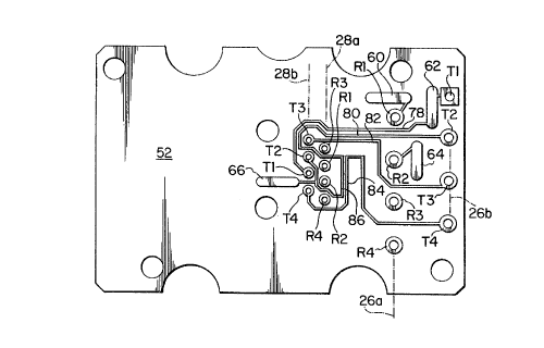
In the embodiment shown in Figure 4, a circuit
assembly 50 is basically similar to that shown in Figure 1
~~~~~J~
7
in that it includes a printed circuit board 52 with a
connector means comprising a connector 22 as described with
reference to Figure 1 arid a modular telephone jack 20 also
as described with reference to Figure 1. The telephone
jack 20 of the embodiment does of course have the tip and
ring positions as already described with reference to
Figure 3. Parasitic reactive couplings are produced by the
conductor paths associated with wires of different pairs
both in the connector 22 and in the telephone jack 20, with
1o the greatest influence on the coupling effects being pro-
vided by the positions of the terminal members in the jack
20 as shown in Figure 3 and as described above.
The circuit assembly of the embodiment in Figure 4
differs from that of the prior art illustrated in Figures 1
and 2 in the fact that the printed circuit board 52 is
provided with compensating reactive means between conductor
paths associated with different pairs of conductor wires of
cable to be connected to the assembly, this compensation
acting against the parasitic reactive coupling in the
2o connector means to significantly reduce the cross-talk
effect in the circuit assembly as a whole.
The compensating reactive coupling is both capaci-
tive and inductive in that capacitors are provided between
certain paths and inductors between certain paths on the
printed circuit board S2. These compensating couplings
will be described with reference to Figures 5a and 5b.
Figure 5a is a direct plan view onto one side of the
printed circuit board 52 and Figure 5b is a mirror image of
the plan view on the other side of the board, the mirror
3o image being provided so that a direct comparison may be
made between the two sides of the board without difficulty.
As may be seen from Figures 5a and 5b, in the
board circuitry, each tip and ring terminal on lines 28a
and 28b is connected by a conductor path with a correspond-
ing tip and ring terminal on the lines 26a and 26b. Capaci-
tive means of the compensating reactive means includes four
capacitors provided by plates formed as part of the printed
s
circuit. One capacitor is formed between the substrate of
the printed circuit board and capacitor plates 60 which are
opposed, one on each side of the substrate as shown by
comparing Figures 5a and 5b. These capacitor plates are
connected one to terminal R1 on line 26a (Figure 5a) and
the other plate 60 is connected to R2 on line 26a (Figure
5b). A second pair of opposed capacitor plates 62 are
connected in the circuitry, one to terminal T1 (Figure 5a)
and the other to terminal T2 (Figure Sb). Third and fourth
io capacitors are provided by a pair of opposed plates 64 and
a pair of opposed plates 66 in combination with the
substrate located between them. The plates 64 are elec-
trically connected one to the R2 terminal in line 26a
(Figure 5a) and the other to the R3 terminal in line 26a
(Figure 5b). The capacitive plates 66 are electrically
connected one to terminal T2 in line 28b (Figure 5a) and
the other to T4 terminal also in line 28b (Figure 5).
Hence, capacitors provided and associated between
terminals T1 T2, R1 R2, R2 R3 and T2 T4, act as a partial
2o compensation against the parasitic coupling provided
respectively between the conductors associated with the
terminals R1 T2, T1 R2, T2 R3 and R2 T4, in the connectors
and 22. However, the capacitive compensation is not
entirely sufficient to compensate for the whole of the
parasitic problem existing between the conductors in the
connectors. To provide the required compensating reactive
coupling the capacitive compensation assists inductive
compensation provided by inductive means on the printed
circuit board. Inductive means comprises an inductor
3o formed between parallel lengths of path 68 and 70 on the
printed circuit board and extending between the two
terminals R1 and the two terminals R2 in the terminal lines
26a and 28a. Inductors are also provided between the
length of path 70 and length of path 72 which extends
between the two R3 terminals on lines 26a and 28a, and
along lengths of path 74 and 76 extending respectively
between the two R2 terminals and the two R4 terminals in
9
lines 26a and 28a. This may be seen from Figure 5b. In
addition, inductors are provided between the tip terminals
along the conductor paths as shown in F~.gure 5a. These
inductors exist between lengths of path 78 and 80 extend-
s ing, respectively, between the two terminals T1 and the two
terminals T2, between the length of path 80 and a length of
path 82 which extends between the two terminals T3, on
lines 26b and 28b, and between lengths of path 84 and 86
extending between the two terminals T2 and the two ter-
1o urinals T4. The parallel lengths of path 78 to 86 and their
distances apart are chosen such that the inductors provide
inductive effects which, when assisted by the capacitors
provided by the plates 60 to 66, substantially compensate
for the parasitic capacitive and inductive coupling in the
15 conductor paths in the connectors which produce the most
serious cross-talk effects.
Figure 6 is an electrical circuit diagram showing
the circuitry through the printed circuit board with the
capacitors and the inductors indicated in the circuitry and
2o identified by the reference numerals for the capacitor
plates and the lengths of paths referred to above with
regard to Figures 5a and 5b.
The following Table shows the parasitic couplings
produced by the conductors passing through the connectors
25 20 and 22 on the left-hand side of the figure, and on the
right-hand side, the compensating capacitors and inductors
provided upon the circuit board 52 are shown. The para-
sitic couplings are shown from line-to-line in decreasing
order of significance for producing cross-talk problems
3o throughout a high frequency line. Thus line A shows the
parasitic couplings which produces the greatest cross-talk
effect. The parasitic couplings shown by line B have a
slighter less effect and those produced by lines C, D and E
have substantially minimal effect. The compensating capaci-
35 tors and inductors shown on the right-hand side of the
Table are provided upon the printed circuit board for the
purpose of substantially compensating for all of the cross-
10
talk problems produced by the parasitic couplings in lines
A and B. As may be seen from the right-hand side of the
table no particular compensating effect is produced for the
parasitic problems shown in lines C, D and E. The reason
for this is that these parasitic couplings produce an
insignificant degree of cross-talk and this may be dis-
regarded in the design of the circuitry for the printed
circuit board.
TABLE
parasitic Reactance om~ensating Reactance
~'~nacitive 'rnd ~ -;
A) R1,T2 ; T1,R2 Tl,T2 ; R1,R2 T1,T2 ; R1,R2
B) T2,R3 ; R2,T4 R2,R3 ; T2,T4 R2,R3 ; R2,R4
T2 , T3 ; T2 , 'r4
C) R1,R3 ; T1,T4 - -
D) R3,T4 - _
E ) T3 , R4 - _
2o As shown by the embodiment above the printed
circuit board 52 has a circuitry with inductive and capaci-
tive compensation for the parasitic coupling effects of the
connectors 20 and 22. The inductive and capacitive compen-
sations act together to substantially eliminate the para-
sitic problems. Thus, in the embodiment, each parasitic
reactance is greater than either of its compensating induc-
tance or compensating capacitance when taken alone.
However, it is possible for the inductance provided between
specific conductor paths on the printed circuit board to
3o substantially compensate fully for any particular parasitic
reactance. In this case the use of a capacitor having
capacitor plates may be avoided. As a further alternative,
the inductance existing between two paths on the printed
circuit board could have an overcompensating effect which
could itself produce cross-talk problems. In such a situa
tion, it would be advantageous to include a capacitor on
11
the printed circuit board which acts against the compensa-
tion and assists the parasitic reactance of the connectors
so as to reduce this cross-talk tendency of the over-
compensating inductive effect.
By way of example, with regard to the latter
situation discussed above, in the embodiment described
there is an inductive effect created along pathways 68 and
70 which extend between the two terminals R1 and the two
terminals R2. Similarly on the other side of the board an
to inductive effect is created along the paths 78 and 80
between the two terminals T1 and the two terminals T2.
These inductive effects axe insufficient to compensate
fully for the parasitic coupling between conductors extend-
ing between the R1 terminals and between the T2 terminals
and between the T1 terminals and the R2 terminals in the
connectors. Hence, the capacitors formed by plates 60 and
62 are required, these plates acting respectively along the
paths extending between the T1 terminals and between the T2
terminals (plates 62) and between the R1 terminals and
2o between the R2 terminals (plates 60). If, however, a
situation arose where the conductor paths 68 and 70 and 78
and 80 produced a compensating effect which was far greater
than the parasitic reactance which required the compensa-
tion, then it would be necessary to replace the capacitors
formed by the plates 60 and 62 with one capacitor acting
between the conductor paths between the two terminals R1
and between the two terminals T2 and another capacitor
between the conductor paths extending between the two
terminals T1 and between the two terminals R2.