Note : Les descriptions sont présentées dans la langue officielle dans laquelle elles ont été soumises.
" CA 02303302 2000-03-03
WO 99/14732 . PCT/US98/17396
High Density Column Drivers for an Active Matrix Display
I. BACKGROUND OF THE INVENTION
1. Technical Field
This invention relates to electronic circuit designs for high density column
drivers for an
active matrix (thin-film transistor) liquid crystal display.
2. Description of Related Art
With recent progress in various aspects of active matrix (thin-film
transistor) liquid
crystal display (LCD) technology, the proliferation of active matrix displays
has been
spectacular in the past several years. In an active matrix display, there is
one transistor or switch
corresponding to each display cell. An active matrix display is operated by
first applying a
selection voltage to a row electrode to activate the bates of that row of
cells. and second
applying appropriate analog data voltages to the column electrodes to charge
each cell in the
I S selected row to a desired voltage Level.
Column drivers are very important circuits in the design of an active matrix
display
panel. The column drivers receive digital display data along with control and
timing signals
from a display controller chip. The column drivers convert the digital display
data to analog
display voltages, typically using one CMOS-based circuit per column to perform
the conversion.
The column drivers then output the analog display voltages onto column
electrodes of the
display.
As the resolution of LCD tlat panel displays (FPDs) increases, the layout area
typically
required by the column driver circuits increases dramatically. For example. as
the resolution of
an LCD FPD increases from 6 bits per primary color (for a total of about 256
thousand colors
possible) to 8 bits per primary color (for a total of about 16 million colors
possible), the layout
area typically required increases by a factor of four (due to the two
additional bits of shading per
primary color).
To alleviate the above described problem, a new circuit and layout scheme for
LCD
column drivers is needed.
II. SUMMARY
SUBSTITUTE SHEET (RULE 26)
CA 02303302 2000-07-26
To reduce the layout area required by LCD column drivers without suffering a
significant decrease in performance, a PMOS-based circuit selects a voltage
from an
upper set of analog display voltages and a NMOS-based circuit selects a
voltage from
a lower set of analog display voltages. This reduces the layout area by up to
roughly a
factor of two compared with conventional column drivers which are CMOS-based.
Moreover, in a typical dot inversion scheme, where two adjacent columns select
voltages from alternating voltage sets, two adjacent columns can share the
same
PMOS-based and NMOS-based circuits by using multiplexers controlled by a
polarity
signal to route the digital display data into the sets of switches. This
reduces the
layout area by up to roughly an additional factor of two.
Accordingly, in one aspect of the present invention there is provided
an electronic circuit for converting a digital value to an analog voltage, the
circuit
comprising:
a first subcircuit for receiving a plurality of upper analog display voltages
and
selecting one of the upper analog display voltages based upon the digital
value, the
first subcircuit containing a larger number of PMOS transistors than NMOS
transistors;
a second subcircuit for receiving a plurality of lower analog display voltages
and selecting one of the lower analog display voltages based upon the digital
value,
the second subcircuit containing a larger number of NMOS transistors than PMOS
transistors;
a multiplexes coupled between the first subcircuit and the second subcircuit
for selecting either the upper analog display voltage or the lower analog
display
voltage.
According to another aspect of the present invention there is provided an
electronic circuit for driving a column electrode of an active matrix display,
the circuit
comprising:
a plurality of lines for communicating a digital display value;
a first set of lines for conducting a set of upper analog voltages above a
midpoint voltage;
a second set of lines for conducting a set of lower analog voltages below the
midpoint voltage;
2
CA 02303302 2000-07-26
a first digital-to-analog converter with more PMOS transistors than NMOS
transistors for selecting from the first set of lines an upper analog voltage
which
corresponds to the digital display value; and
a second digital-to-analog converter with more NMOS transistors than PMOS
transistors for selecting from the second set of lines a lower analog voltage
which
corresponds to the digital display value.
According to another aspect of the present invention there is provided an
electronic circuit for driving a pair of columns of an active matrix display,
the circuit
comprising:
a first plurality of lines communicating a first digital display value
associated
with a first column of the display;
a second plurality of lines communicating a second digital display value
associated with a second column of the display;
a polarity signal with a high state and a low state;
a first set of multiplexers coupled to the first and second pluralities of
lines,
the first set of multiplexers selecting the first digital display value if the
polarity signal
is in the high state, and selecting the second digital display value if the
polarity signal
is in the low state; and
a second set of multiplexers coupled to the first and second pluralities of
lines,
the second set of multiplexers selecting the first digital display value if
the polarity
signal is in the low state, and selecting the second digital display value if
the polarity
signal is in the high state.
According to another aspect of the present invention there is provided a
method for driving a column of an active matrix display, the method comprising
the
steps of:
receiving a digital value and a polarity signal;
using a first set of transistors to select an upper analog voltage from a set
of
upper analog voltages as a function of the received digital value, wherein the
first set
of transistors is comprised of more PMOS than NMOS transistors;
using a second set of transistors to select a lower analog voltage from a set
of
lower analog voltages as a function of the received digital value, wherein the
second
set of transistors is comprised of more NMOS than PMOS transistors;
2a
CA 02303302 2000-07-26
driving the column of the active matrix display with the upper analog voltage
if the polarity signal is in a first state; and
driving the column of the active matrix display with the lower analog voltage
if the polarity signal is in a second state.
According to another aspect of the present invention there is provided a
method for driving a pair of columns of an active matrix display, the method
comprising the steps of:
receiving a polarity signal capable of being in either a first state or a
second
state; and
routing a first digital display value associated with a first column in the
pair of
columns to a first digital-to-analog converter and a second digital display
value
associated with a second column in the pair of columns to a second digital-to-
analog
converter when the polarity signal is in the first state, wherein the first
digital-to-
analog converter is comprised of a plurality of PMOS transistors and the
second
digital-to-analog converter is comprised of a plurality of NMOS transistors;
or
routing the first digital display value to the second digital-to-analog
converter
and the second digital display value to the first digital-to-analog converter
when the
polarity signal is in the second state, wherein the first digital-to-analog
converter
includes a plurality of PMOS transistors and the second digital-to-analog
converter
includes a plurality of NMOS transistors.
III. BRIEF DESCRIPTION OF THE DRAWINGS
Embodiments of the present invention will now be described more fully with
reference to the accompanying drawings in which:
Figure 1 is a schematic diagram of a first and conventional column driver
circuit with a CMOS-based circuit used as a digital-to-analog converter.
Figure 2A is an illustrative graph of LCD transmission (brightness) as a
function of the analog display voltage on a column electrode.
Figure 2B is a schematic diagram of a first and conventional CMOS-based
circuit used as a digital-to-analog converter.
2b
CA 02303302 2000-07-26
Figure 2C is a schematic diagram of a second and conventional CMOS-based
circuit with a decoder circuit.
Figure 3 is a schematic diagram of a second and alternate column driver
circuit with a PMOS-based circuit and a NMOS-based circuit according to the
present
invention.
Figure 4A is a schematic diagram of a first and preferred PM OS-based circuit
according to the present invention.
Figure 4B is a schematic diagram of a second and alternate mostly-PMOS-
based circuit according to the present invention.
Figure 4C is a schematic diagram of a first and preferred NMOS-based circuit
according to the present invention.
Figure 4D is a schematic diagram of a second and alternate mostly-NMOS-
based circuit according to the present invention.
2c
CA 02303302 2000-03-03
WO 99/14732 PCT/US98/17396
Figure 4E is a schematic diagram of a third and alternate PMOS-based circuit
according
to the present invention.
Figure 4F is a schematic diagram of a fourth and alternate mostly-PMOS-based
circuit
according to the present invention.
Figure 4G is a schematic diagram of a third and alternate NMOS-based circuit
according
to the present invention.
Figure 4H is a schematic diagram of a fourth and alternate mostly-NMOS-based
circuit
according to the present invention.
Figure 5 is a schematic diagram of a third and preferred column driver circuit
which
multiplexes the input into the PMOS-based and NMOS-based circuits according to
the present
invention.
Fig. 6 is a schematic diagram of a fourth and preferred column driver circuit
with a
cascaded structure to deal with 4-bit display data according to the present
invention.
Fig. 7 is a schematic diagram of a fifth and conventional column driver
circuit which
accommodates row, but not dot. inversion.
Fig. 8 is a schematic diagram of a conventional CMOS-based circuit for use in
the fifth
and conventional column driver circuit.
Fig. 9 is a schematic diagram of a sixth and alternate column driver circuit
which
accommodates row, but not dot. inversion according to the present invention.
Fig. 10 is a schematic diagram of the NMOS/CMOS circuit for use in the sixth
and
alternate column driver circuit according to the present invention.
IV. DESCRIPTION OF THE PREFERRED EMBODIMENTS
A. Prior Art f Dot Inversion)
Figure 1 is a schematic diagram of a first and conventional column driver
circuit 100
with CMOS-based circuits 111 used as digital-to-analog converters. The first
column driver
circuit 100 is shown for two adjacent columns of a display, column X and
column X+1. For
SUBSTITUTE SHEET (RULE 26)
CA 02303302 2000-03-03
WO 99114732 PCT1US98/17396
purposes of clarity in this description. a two-bit version of the first column
driver circuit 100 is
shown.
For each column, a shift resister 102 receives serial digital display data
from a panel
controller chip (not shown) and outputs the digital display data in parallel
form to a
conventional CMOS-based circuit 1 1 1. Since Fig. 1 illustrates a two-bit
version of the first
column driver circuit 100, each shift register 102 outputs two bits (via two
lines). The two bits
output by the shift register 102 corresponding to column X are denoted Ao and
A,, where A~ is
the low order bit, and A, is the high order bit, of the two-bit digital
display value for column X.
A~ is output on a first digital line 104, and A, is output on a second digital
line 106. When A~ is
low, the first digital line 104 carries 0 volts. When A" is high, the first
digital Line 104 carries
l0 volts. Similarly, when A, is low. the second digital line 106 carries 0
volts. When A, is
high, the second digital line 1 10 carries 10 volts. Both the first l04 and
second 106 digital lines
connect to a left CMOS-based circuit l 1 1. Similarly. the two bits output by
the shift register
102 corresponding to column X+1 are denoted B« and B,, where B~ is the low
order bit and B,
is the high order bit of the two-bit digital display value for column X+l. B~
is output on a third
digital line 108, and B~ is output on a fourth digital line 1 10. Both the
third l08 and fourth I 10
digital lines connect to a right CMOS-based circuit 1 1 1 which is typically
identical in design to
the left CMOS-based circuit I 1 1.
A group of eight (2°+~, where n = the number- of bits per digital
display value) analog
display voltages (i.e., analog reference voltages) is received by each CMOS-
based circuit 1 1 1.
The group of analog display voltages may be divided into two sets: an upper
voltage set 1 13
and a lower voltage set 114. The upper voltage set 1 l 3 provides reference
voltages at or above a
midpoint voltage. while the lower voltage set 1 14 provides reference voltages
at or below the
midpoint voltage. The upper and lower voltage sets 113 and I 14 are
approximately symmetrical
across the midpoint voltage, and the midpoint voltage is connected to the
backside electrode of
the display panel. For the first column driver circuit l00 shown in Fig. l,
the midpoint voltage
is five volts (5 V). The upper voltage set 1 13 comprises: 5 V; 5 V plus 0X; 5
V plus ~Y and
ten volts ( 10 V). The voltage values for AX and 0Y are such that 0 V < AX <
DY < 5 V.
Similarly, the lower voltage set 1 14 comprises: 5 V: 5 V minus ~?C; 5 V minus
DY; and 0 V.
The upper 1 13 and lower 1 14 voltage sets input into each CMOS-based circuit
1 1 1 or 112 are
further described below in relation to Fia. 2A.
SUBSTITUTE SHEET (RULE 26j
CA 02303302 2000-03-03
WO 99/14732 PCT/US98/17396
Each CMOS-based circuit 1 I 1 selects an upper voltage from the upper voltage
set I 13
and a corresponding lower voltage from the lower voltage set 114. The upper
voltage selected
by the left CMOS-based circuit 1 I 1 (for column X) is output on a first
analog line 1 l6. The
lower voltage selected by the left CMOS-based circuit 11 1 is output onto a
second analog line
1 18. The upper voltage selected by the right CMOS-based circuit I l 1 (for
column X+1) is
output on a third analog line 120. The lower voltage selected by the right
CMOS-based circuit
111 is output onto a fourth analog line 122. Two conventional designs for the
CMOS-based
circuit which is a set of CMOS switches t 11 are further described below in
relation to Figs. 2B
and 2C.
A first multiplexes 124 and a second multiplexes 126 are controlled by a
polarity signal
128. The first 116 and second I 18 analog lines connect to the inputs of the
first multiplexes 124
so that the first multiplexes 124 can select either the upper voltage on the
first analog line I 16 or
the lower voltage on the second analog line 118 depending on the value of the
polarity signal
128. If the polarity signal 128 is high ( 1 ), then the first multiplexes 124
selects the upper
voltage on the first analog line 116. If the polarity signal 128 is low (0),
then the first
multiplexes 124 selects the lower voltage on the second analog line 118.
Similarly, the third
120 and fourth 1?2 analog lines connect to the inputs of the second
multiplexes 126 so that the
second multiplexes 126 can select either the upper voltage on the third analog
line 120 or the
lower voltage on the fourth analog line 122 depending on the value of the
polarity signal 128. If
the polarity signal 128 is high ( 1 ), then the second multiplexes 126 selects
the lower voltage on
the fourth analog line 122. If the polarity signal 128 is low (0), then the
second multiplexes 126
selects the upper voltage on the third analog line 120.
Thus, when the polarity signal 128 is high ( 1 ), the first multiplexes 124
selects an upper
voltage while the second multiplexes l26 selects a lower voltage. Similarly,
when the polarity
signal 128 is low (0), the first multiplexes 124 selects a lower voltage while
the second
multiplexes 126 selects an upper voltage. This "inversion" between adjacent
pixels in a row is
done by design in order to reduce display flicker and crosstalk between
columns. This inversion
scheme is called dot-inversion.
The voltage selected by the first multiplexes 124 is output to the column
electrode for
column X 130. The voltage selected by the second multiplexes l26 is output to
the column
electrode for column X+1 132.
5
SUBSTITUTE SHEET (RULE 26)
CA 02303302 2000-03-03
WO 99114732 PCT/US98/17396
For each row selected (activated by application of a selection voltage to the
row
electrode), the polarity signal ( 28 applied by the first column driver
circuit 100 is either high ( l )
or low (0). However. between the selection of adjacent rows, the polarity
signal 128 is typically
switched from high to low, or from low to high. This "inversion" between
adjacent rows is
done in order to reduce display flicker and crosstalk between rows. This
inversion scheme is
called line-inversion. A dot-inversion scheme usually incorporates fine-
inversion as well.
In addition, between the display of adjacent frames (scanning periods), the
polarity
signal 128 for the first row is typically switched from high to low, or from
low to high. This
''inversion" between adjacent frames is done in order to reduce display
Clicker and crosstalk
between frames. This inversion scheme is called frame inversion. Most of the
LCD based
displays use frame inversion.
The first column driver circuit 100 described above has the capability to
provide analog
voltages both above and below the backside electrode voltage of ~V at the same
time. but not all
conventional column driver circuits are so enabled. Other conventional column
driver circuits,
which adopt line inversion, but not dot inversion, can provide analog voltages
which alternate
between being above and below the backside electrode voltage. This is
typically done by
flipping the arrangement of analog voltages on the lines in conjunction with
alternating the
backside voltage between low and high voltages (see Fig. 7, discussed in
detail below).
Figure 2A is an illustrative graph of LCD transmissivity (brightness) as a
function of
analog display voltage on a column electrode 130 or 132. The graph depicts a
typical nonlinear
curve where LCD transmissivitv peaks near one when the analog display voltage
is at the
midpoint voltage (5V) and decreases to about zero as the difference between
the analog display
voltage and the midpoint voltage increases.
It is desirable to select the upper 1 13 and lower 1 I4 sets of analog display
voltages so
that they correspond to transmissivity levels which are relatively evenly
spaced. Fig. 2A shows
an upper set 113 comprising analog display voltages of SV, SV + OX, SV + DY,
and 10 V that
are shown to correspond to transmissivity levels of about 1, 2/3, 1/3, and 0,
respectively. Fig.
2A also shows a lower set l 14 comprising analog display voltages of SV, SV -
~X, SV - ~Y,
and 0V that are shown to correspond to transmissivity levels of about l, 2/3,
1/3, and 0,
respectively. If the transrnissivity function is not symmetrical about the
midpoint voltage, the
6
SUBSTITUTE SHEET (RULE 26)
CA 02303302 2002-10-17
analog display voltages can be adjusted to maintain relatively evenly-spaced
transmissivity levels.
Figure 2B is a schematic diagram of the first and conventional CMOS-based
circuit 111 used as a digital-to-analog converter. The first CMOS-based
circuit 111
comprises two inverters 201 and 202, and twelve CMOS switches 205, 208, 212,
215,
218, 222, 225, 228, 232, 235, 238, and 242.
The low order bit Ao for column X (or the low order bit Bo for column X + 1)
is input along the first digital line 104 (or the third digital line 108) into
a first inverter
201 which inverts the low order bit Ao and outputs Ao', where prime denotes an
inverse or complement. Similarly, the high order bit Al for column X (or the
high
order bit B ~ for column X + 1 ) is input along the second digital line 106
(or the fourth
digital line 110) into a second inverter 202 which inverts the low order bit
Ao and
outputs Ao'.
Regarding the three CMOS switches 205, 208, and 212 in the top quarter
portion of Fig. 2B, the first digital line 104 (or the third digital line 108)
is connected
to the gate electrode of a first NMOS transistor 203, and the output of the
first inverter
201 is connected to the gate electrode of a first PMOS transistor 204. The
highest
voltage (10 V) in the upper voltage set 113 is connected to the source of both
the first
NMOS 203 and the first PMOS 204 transistors. Together, the first NMOS
transistor
203 and the first PMOS transistor 204 comprise a first CMOS switch 205. When
the
low order bit Ao is high (1), then the first CMOS switch 205 is "on," meaning
that the
first CMOS switch 205 drives its output (the drain voltage) to 10 V.
The first digital line 104 is connected to the gate electrode of a second PMOS
transistor 206, and the output of the first inverter 201 is connected to the
gate
electrode of a second NMOS transistor 207. The second highest voltage (5V +
~Y) in
the upper voltage set 113 is connected to the source of both the second PMOS
206
and the second NMOS 207 transistors. Together, the second PMOS 206 and the
7
CA 02303302 2002-10-17
second NMOS 207 transistors comprise a second CMOS switch 208. When the low
order bit Ao is low (0), then the second CMOS switch 208 is "on," meaning that
the
second CMOS switch 208 drives its output (the drain voltage) to S V + 0Y.
The outputs of the first 205 and the second 208 CMOS switches are connected
together by a first intermediate line 209. Thus, when the low order bit Ao is
high, the
first intermediate
7a
CA 02303302 2000-03-03
WO 99/14732 PCT/US98/17396
line 209 is driven by the first CMOS switch 205 to l0 V, and when the low
order bit A~ is low,
the first intermediate line 209 is driven by the second CMOS switch ?08 to ~ V
+,~Y.
The second digital line 106 (or the fourth digital line I 10) is connected to
the gate
electrode of a third NMOS transistor '? 10. and the output of the second
inverter 202 is connected
to the gate electrode of a third PMOS transistor 211. The first intermediate
line 209 is
connected to the source of both the third NMOS 2 I0 and the third PMOS 211
transistors.
Together, the third NMOS transistor 210 and the third PMOS transistor 211
comprise a third
CMOS switch 212. When the high order bit A, is high ( 1 ), then the third CMOS
switch 212 is
"on," meaning that the third CMOS switch 212 drives its output (the drain
voltage) to same
voltage as that on the first intermediate line 209.
Regarding the three CMOS switches 215, 218, and 2''2 in the second-from-the-
top
quarter portion of Fig. 2B. the first digital line 104 (or the third digital
line 1081 is connected to
the gate electrode of a fourth NMOS transistor 213, and the output of the
first inverter 201 is
connected to the gate electrode of a fourth PMOS transistor 214. The third
highest voltage (5 V
I S + OX) in the upper voltage set l 13 is connected to the source of both the
fourth NMOS 213 and
the fourth PMOS 214 transistors. Together, the fourth NMOS transistor 213 and
the fourth
PMOS transistor 214 comprise a fourth CMOS switch 2 I5. When the low order bit
Ao is high
( 1 ), then the fourth CMOS switch 215 is "on," meaning that the fourth CMOS
switch 215 drives
its output (the drain voltage) to 5 V + ~X.
The first digital line 104 is also connected to the gate electrode of a fifth
PMOS
transistor 216, and the output of the first inverter 201 is also connected to
the gate electrode of a
fifth NMOS transistor 217. The lowest voltage SV in the upper voltage set 113
is connected to
the source of both the fifth PMOS 216 and the fifth NMOS 217 transistors.
Together, the fifth
PMOS 216 and the fifth NMOS 217 transistors comprise a fifth CMOS switch 218.
When the
low order bit A~ is low (0), then the fifth CMOS switch 218 is "on," meaning
that the fifth
CMOS switch 218 drives its output (the drain voltage) to 5 V.
The outputs of the fourth 215 and the fifth 218 CMOS switches are connected
together
by a second intermediate line 219. Thus. when the low order bit A« is high,
the second
intermediate line 219 is driven by the fourth CMOS switch 215 to ~ V + OX, and
when the low
order bit A~> is low. the'second intermediate line 219 is driven by the fifth
CMOS switch 218 to
5 V.
8
SUBSTITUTE SHEET (RULE 26)
.
CA 02303302 2000-03-03
WO 99/14732 PCT/US98/17396
The second digital line 106 (or the fourth digital line 110) is connected to
the gate
electrode of a sixth PMOS transistor 220, and the output of the second
inverter 202 is connected
to the gate electrode of a sixth NMOS transistor 221. The second intermediate
line 219 is
connected to the source of both the sixth PMOS 220 and the sixth NMOS 221
transistors.
Together, the sixth PMOS transistor 220 and the sixth NMOS transistor 221
comprise a sixth
CMOS switch 222. When the high order bit A, is low (0), then the sixth CMOS
switch 222 is
"on," meaning that the sixth CMOS switch 222 drives its output (the drain
voltage) to same
voltage as that on the second intermediate line 219.
Regarding the output of the top half of Fig. 2B, the output (drain voltage) of
both the
third CMOS 212 and the sixth CMOS 222 switches are connected to the first
analog line 116 (or
the third analog line 120). Thus, when Ao = 1 and A, = l, then 10 V is driven
onto the first
analog line 116. When A~ = 0 and A, = 1, then 5 V + DY is driven onto the
first analog line
116. When A,> = 1 and A, = 0, then 5 V + OX is driven onto the first analog
line 116. Lastly,
when A~ = 0 and A, = 0, then 5 V is driven onto the first analog line 1 l6.
Regarding the three CMOS switches 225, 228, and 232 in the bottom quarter
portion of
Fig. 2B, the first digital line 104 (or the third digital line 108) is
connected to the gate electrode
of a seventh NMOS transistor 223, and the output of the first inverter 201 is
connected to the
gate electrode of a seventh PMOS transistor 224. The lowest voltage (0 V) in
the lower voltage
set 114 is connected to the source of both the seventh NMOS 223 and the
seventh PMOS 224
transistors. Together, the seventh NMOS transistor 223 and the seventh PMOS
transistor 224
comprise a seventh CMOS switch 225. When the low order bit A~, is high ( 1 ),
then the seventh
CMOS switch 225 is "on,'' meaning that the seventh CMOS switch 225 drives its
output (the
drain voltage) to 0 V.
The first digital Line 104 is connected to the gate electrode of a eighth PMOS
transistor
226, and the output of the first inverter 201 is connected to the gate
electrode of a eighth NMOS
transistor 227. The second lowest voltage (5 V - DY) in the lower voltage set
114 is connected
to the source of both the eighth PMOS 226 and the eighth NMOS 227 transistors.
Together, the
eighth PMOS 226 and the eighth NMOS 227 transistors comprise a eighth CMOS
switch 228.
When the low order bit A~ is low (0), then the eighth CMOS switch 228 is "on,"
meaning that
the eighth CMOS switch 228 drives its output (the drain voltage) to 5 V - ~Y.
9
SUBSTITUTE SHEET (RULE 26)
CA 02303302 2000-03-03
WO 99/14732 PCT/US98/17396
The outputs of the first 22~ and the second 228 CLIOS switches are connected
together
by a third intermediate line 229. Thus, when the low order bit A" is high, the
third intermediate
line 229 is driven by the seventh CMOS switch 22~ to 0 V. and when the Iow
order bit A~ is
low, the third intermediate line 229 is driven by the eighth CMOS switch 228
to 5 V - DY.
The second digital line 106 (or the fourth digital line 1 10) is connected to
the gate
electrode of a ninth NMOS transistor 230, and the output of the second
inverter 202 is
connected to the gate electrode of a ninth PMOS transistor 231. The third
intermediate line 229
is connected to the source of both the ninth NMOS 230 and the ninth PMOS 231
transistors.
Together, the ninth NMOS transistor 230 and the ninth PMOS transistor 231
comprise a ninth
CMOS switch 232. When the high order bit A, is high ( 1 ), then the ninth CMOS
switch 232 is
"on," meaning that the ninth CMOS switch 232 drives its output (the drain
voltage) to same
voltage as that on the third interTnediate line 229.
Regarding the three CMOS switches 235. 238, and 242 in the second-from-the-
bottom
quarter portion of Fig. 2B, the first digital line 104 (or the third digital
line 108) is connected to
IS the gate electrode of a tenth NMOS transistor 233, and the output of the
first inverter 20I is
connected to the gate electrode of a tenth PMOS transistor 234. The third
lowest voltage (5 V -
OX) in the lower voltage set 1 I4 is connected to the source of both the tenth
NMOS 233 and the
tenth PMOS 234 transistors. Together, the tenth NMOS transistor 233 and the
tenth PMOS
transistor 234 comprise a tenth CMOS switch 235. When the low order bit A~> is
high ( 1 ), then
the tenth CMOS switch 235 is "on." meaning that the tenth CMOS switch 235
drives its output
(the drain voltage) to 5 V - 0X.
The first digital line 104 is also connected to the gate electrode of a
eleventh PMOS
transistor 236, and the output of the first inverter 201 is also connected to
the gate electrode of a
eleventh NMOS transistor 237. The highest voltage 5 V in the lower voltage set
t 14 is
connected to the source of both the eleventh PMOS 236 and the eleventh NMOS
237 transistors.
Together, the eleventh PMOS 236 and the eleventh NMOS 237 transistors comprise
a eleventh
CMOS switch 238. When the low order bit Ao is low (0), then the eleventh CMOS
switch 238
is "on," meaning that the eleventh CMOS switch 238 drives its output (the
drain voltage) to 5 V.
The outputs of the fourth 235 and the fifth 238 CMOS switches are connected
together
by a fourth intermediate fine 239. Thus, when the low order bit A,~ is high,
the fourth
intermediate line 239 is driven by the tenth CMOS switch 235 to 5 V - 0X, and
when the low
to
SUBSTITUTE SHEET (RULE 26)
CA 02303302 2000-03-03
WO 99/14732 PCT/US98/17396
order bit A~ is low, the fourth intermediate line 239 is driven by the
eleventh CMOS switch 238
to 5 V.
The second digital line 106 (or the fourth digital line i08) is connected to
the gate
electrode.of a twelfth PMOS transistor 240, and the output of the second
inverter 202 is
connected to the gate electrode of a twelfth NMOS transistor 241. The fourth
intermediate line
239 is connected to the source of both the twelfth PMOS 240 and the twelfth
NMOS 241
transistors. Together, the twelfth PMOS transistor 240 and the twelfth NMOS
transistor 241
comprise a twelfth CMOS switch 242. When the high order bit A, is low (0),
then the twelfth
CMOS switch 242 is "on," meaning that the twelfth CMOS switch 242 drives its
output (the
drain voltage) to same voltage as that on the fourth intermediate line 239.
Regarding the output of the bottom half of Fig. 2B, the output (drain voltage)
of both the
ninth CMOS 232 and the twelfth CMOS 2=l? switches are connected to the second
analog line
118 (or the fourth analog line 1?2). Thus, when Ao = 1 and A, = 1, then 0 V is
driven onto the
second analog line 118. When Ao = 0 and A, = 1, then 5 V - AY is driven onto
the second
analog line 1 18. When A~ = 1 and A, = 0, then 5 V - ~X is driven onto the
second analog line
118. Lastly, when A~ = 0 and A, = 0, then 5 V is driven onto the second analog
line 118.
Figure 2C is a schematic diagram of a second and conventional CMOS-based
circuit ! 11
with a decoder circuit 252. The second CMOS-based circuit 111 comprises a
decoder circuit
252. four inverters 257-260, and eight CMOS switches 263, 266. 269, 27?. 283,
286, 289. and
?0 292.
The decoder circuit 252 receives .the low order bit A~ for column X along the
first digital
line 104 and the high order bit A, for column X along the second digital line
106 (or the low
order bit Bo for column X+1 along the third digital line 108 and the high
order bit B, for column
X+1 along the fourth digital line 110). The decoder circuit 252 performs a
logical AND
operation on the high order bit A, and the low order bit A~, and it outputs
the result A,Ao on a
first decoded line 253. The decoder circuit 252 also performs a logical AND
operation on the
high order bit A, and the complement of the low order bit Ao, and it outputs
the result A,Ao'
(where prime denotes the complement) on a second decoded line 254. The decoder
circuit 252
also performs a logical AND operation on the complement of the high order bit
A, and the low
order bit Ao, and it outputs the result A,'A~ on a third decoded line 255. The
decoder circuit
252 also performs a logical AND operation on the complement of the high order
bit A, and the
SUBSTITUTE SHEET (RULE 26)
CA 02303302 2002-10-17
complement of the low order bit Ao, and it outputs the result AI'Ao' on a
fourth
decoded line 256.
The result AIAo on the first decoded line 253 is input into a first inverter
257
which outputs the complement of A~Ao, i.e. it outputs (Al'Aq'). The result
AIA.o' on
the second decoded line 254 is input into a second inverter 258 which outputs
(Al'Ao). The result A1'Ao on the third decoded line 255 is input into a third
inverter
259 which outputs (A~Ao'). The result AI'Ao' on the fourth decoded line 256 is
input
into a fourth inverter 260 which outputs (AIAo).
Regarding the four CMOS switches 263, 266, 269, and 272 in the top half of
Fig. 2C, the first decoded line 253 is connected to the gate electrode of a
first NMOS
transistor 261, and the output of the first inverter 257 is connected to the
gate of a first
PMOS transistor 262. The highest voltage (10 V) in the upper voltage set 113
is
connected to the source of both the first NMOS 261 and the first PMOS 262
transistors. Together, the first NMOS transistor 261 and the first PMOS
transistor 262
comprise a first CMOS switch 263. When the first decoded line 253 is high
(i.e., A o =
1 AND A, = 1 ), then the first CMOS switch 263 is "on," meaning that the first
CMOS
switch 263 drives its output (the drain voltage) to 10 V.
The second decoded line 254 is connected to the gate electrode of a second
NMOS transistor 264, and the output of the second inverter 258 is connected to
the
gate of a second PMOS transistor 265. The second highest voltage (5 V + 0y) in
the
upper voltage set 113 is connected to the source of both the second NMOS 264
and
the second PMOS 265 transistors. Together, the second NMOS transistor 264 and
the
second PMOS transistor 265 comprise a second CMOS switch 266. When the second
decoded line 254 is high (i.e., Ao= 0 AND A1= 1), then the second CMOS switch
266
is "on," meaning that the second CMOS switch 266 drives its output (the drain
voltage) to 5 V + DY.
The third decoded line 255 is connected to the gate electrode of a third NMOS
12
CA 02303302 2002-10-17
transistor 267, and the output of the third inverter 259 is connected to the
gate of a
third PMOS transistor 268. The third highest voltage (5 V + 0X) in the upper
voltage
set 113 is connected to the source of both the third NMOS 267 and the third
PMOS
268 transistors. Together, the third NMOS transistor 267 and the third PMOS
transistor 268 comprise a third CMOS switch 269. When the third decoded line
255 is
high (i.e., A o = 1 AND Al = 0), then the third CMOS switch
12a
CA 02303302 2000-03-03
WO 99114732 PCT/US98/17396
269 is "on." meaning that the third CMOS switch 269 drives its output (the
drain voltage) to 5 V
+ OX.
The fourth decoded line 256 is connected to the gate electrode of a fourth
NMOS
transistor 270, and the output of the fourth inverter 260 is connected to the
gate of a fourth
PMOS transistor 271. The lowest voltage 5 V in the upper voltage set 113 is
connected to the
source of both the fourth NMOS 270 and the fourth PMOS 271 transistors.
Together, the fourth
NMOS transistor 270 and the fourth PMOS transistor 271 comprise a fourth CMOS
switch 272.
When the fourth decoded line 256 is high (i.e., Ao = 0 AND A, = 0), then the
fourth CMOS
switch 272 is "on," meaning that the fourth CMOS switch 272 drives its output
(the drain
voltage) to 5 V.
Regarding the output of the top half of Fig. 2C, the outputs (drain voltage)
of the first
263, second 266, third 269, and fourth 272 CMOS switches are all connected to
the first analog
line 116 (or the third analog line 120). Thus, when Ao = I and A, = 1. then l0
V is driven onto
the first analog line 116. When A" = 0 and A, = 1, then 5V + DY is driven onto
the first analog
line 116. When A~ = 1 and A, = 0, then 5 V + 0X is driven ontd the first
analog line 116.
Lastly, when A~ = 0 and A, = 0, then 5 V is driven onto the first analog line
116.
Regarding the four CMOS switches 283, 286, 289, and 292 in the bottom half of
Fig.
2C, the first decoded line 253 is connected to the gate electrode of a fifth
NMOS transistor 281,
and the output of the first inverter 257 is connected to the Gate of a fifth
PMOS transistor 282.
The lowest voltage (0 V) in the lower voltage set 1 14 is connected to the
source of both the fifth
NMOS 281 and the fifth PMOS 282 transistors. Together, the fifth NMOS
transistor 281 and
the fifth PMOS transistor 282 comprise a fifth CMOS switch 283. When the first
decoded line
253 is high (i.e., Ao = 1 AND A, = 1 ), then the fifth CMOS switch 283 is
"on," meaning that the
fifth CMOS switch 283 drives its output (the drain voltage) to 0 V.
The second decoded line 254 is connected to the gate electrode of a sixth NMOS
transistor 284, and the output of the second inverter 258 is connected to the
gate of a sixth
PMOS transistor 285. The second lowest voltage (5 V - ~Y) in the lower voltage
set 114 is
connected to the source of both the sixth NMOS 284 and the sixth PMOS 285
transistors.
Together, the sixth NMOS transistor 284 and the sixth PMOS transistor 285
comprise a sixth
CMOS switch 286. WHen the second decoded line 254 is high (i.e.. AD = 0 AND Ai
= 1), then
~3
SUBSTITUTE SHEET (RULE 26)
CA 02303302 2000-03-03
WO 99/14732 PCT/US98/17396
the sixth CMOS switch ?86 is "on." meaning that the sixth CMOS switch 286
drives its output
(the drain voltage) to 5 V - ~Y.
The third decoded line 25~ is connected to the gate electrode of a seventh
NMOS
transistor 287, and the output of the third inverter 259 is connected to the
gate of a seventh
3 PMOS transistor 288. The third lowest voltage (5 V - ~X) in the lower
voltage set 114 is
connected to the source of both the seventh NMOS 287 and the seventh PMOS 288
transistors.
Together, the seventh NMOS transistor 287 and the seventh PMOS transistor 288
comprise a
seventh CMOS switch 289. When the third decoded line 255 is high (i.e., Ao = 1
A~~1D A, = 0),
then the seventh CMOS switch 289 is "on," meaning that the seventh CMOS switch
289 drives
its output (the drain volta;e) to 5 V - ~.
The fourth decoded line 256 is connected to the gate electrode of a eighth
NMOS
transistor 290, and the output of the fourth inverter 260 is connected to the
gate of a eighth
PMOS transistor 291. The highest voltage 5 V in the lower voltage set 1 14 is
connected to the
source of both the eighth NMOS 290 and the eighth PMOS 291 transistors.
Together, the eighth
NMOS transistor 290 and the eighth PMOS transistor 291 comprise a eighth CMOS
switch 292.
When the fourth decoded line 256 is high (i.e., A~ = 0 AND A, = 0), then the
eighth CMOS
switch 292 is "on," meaning that the eighth CMOS switch 292 drives its output
(the drain
voltage) to 5 V.
Regarding the output of the bottom half of Fig. ~C, the outputs (drain
voltage) of the
?0 fifth 283, sixth 286, seventh 289. and eighth 292 CMOS switches are all
connected to the
second analog line 118 (or the fourth analog line 122). Thus. when A~ = l and
A, = l, then 0 V
is driven onto the second analog line 1 ! 8. When A~ = 0 and A, = 1, then SV -
~Y is driven onto
the second analog Iine 118. When Ao = 1 and A, = 0, then ~ V - AX is driven
onto the second
analog line 118. Lastly, when A~ = 0 and A, = 0, then 5 V is driven onto the
second analog line
1 I 8.
B. Present Invention (Dot Inversion)
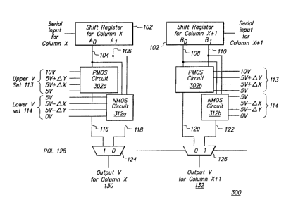
Figure 3 is a schematic diagram of a second column driver circuit 300 with a
PMOS-
based circuit 302 and a NMOS-based circuit 312 according to the present
invention. The second
column driver circuit 300 is shown for two adjacent columns of a display,
column X and column
14
SUBSTITUTE SHEET (RULE 26)
CA 02303302 2000-03-03
WO 99/14732 PCT/US98/17396
X+1. For purposes of clarity in this description, a two-bit version of the
second column driver
circuit 300 is shown.
For each column, a shift register 102 receives serial digital display data
from a panel
controller chip (not shown) and outputs the digital display data in parallel
form to a PMOS-
S based circuit 302 and a NMOS-based circuit 312. Since Fig. 3 illustrates a
two-bit version of
the second column driver circuit 300, each shift register 102 outputs two bits
(via two lines).
The two bits output by the shift register 102 corresponding to column X are
denoted A~ and A,,
where A~ is the low order bit, and A, is the high order bit. of the two-bit
digital display value for
column X. Those skilled in the art would understand how this could be expanded
for any
number of columns (X+2, X+3, ..., X+n) and the description of only tow columns
is provided
for clarity and ease of understanding. A~ is output on a first digital tine
104, and A, is output on
a second digital line 106. The first digital line 104 connects to a first
input of a left PMOS-
based circuit 302a (for column X) and to a first input of a lent NMOS-based
circuit 312a lfor
column X). The second digital line 106 connects to a second input of the left
PMOS-based
circuit 302a and to a second input of the left NMOS-based circuit 312x.
Similarly, the two bits
output by the shift register 102 corresponding to column X+1 are denoted B~
and B,, where B~
is the low order bit, and B, is the high order bit, of the two-bit digital
display value for column
X+l. Bo is output on a third digital line 108, and B, is output on a fourth
digital line 110. The
third digital line 108 connects to a first input of a right PMOS-based circuit
302b (for column
X+1) and to a first input of a right NMOS-based circuit 312b (for column X+1).
The fourth
digital line I l0 connects to a second input of the ri;ht PMOS-based circuit
302b and to a second
input of the right NMOS-based circuit 312b.
An upper voltage set 113 of four (2", where n = the number of bits per digital
display
value) analog display voltages (i.e., analog reference voltages) at or above a
midpoint voltage is
received by each PMOS-based circuit 302. For the second column driver circuit
300 shown in
Fig. 3, the midpoint voltage is five volts (S V) and the upper voltage set 113
comprises: 5 V; 5
V plus ~X; 5 V plus ~Y and 10 V. The voltage values for OX and DY are such
that 0 V < ~X <
DY < 5 V. PMOS switches are typically good at switching such upper voltage
levels. Similarly,
a lower voltage set 114 of four (2", where n = the number of bits per digital
display value)
analog display voltages (i.e.. analog reference voltages) at or below the
midpoint voltage is
received by each NMOS-based circuit 302. For the second column driver circuit
300 shown in
Fig. 3, the lower voltage set 1 14 comprises: 5 V: 5 V minus ~1X: 5 V minus ~Y
and 0 V.
SUBSTITUTE SHEET (RULE 26)
CA 02303302 2000-03-03
WO 99/14732 PCT/US98/17396
NMOS switches are typically ;ood at switching such lower voltage levels. The
upper and lower
voltage sets I 13 and 1 14 are approximately symmetrical about the midpoint
voltage and are
further described above in relation to Fia. 2A.
Each PMOS-based circuit 302 selects an upper voltage from the upper voltage
set 113.
The left PMOS-based circuit 302 (for column X) outputs the selected upper
voltage onto a first
analog line 116, and the right PMOS-based circuit 302 (for column X+1 )
outputs the selected
upper voltage onto a third analog line 120. Similarly, each NMOS-based circuit
312 selects a
lower voltage from the lower voltage set 114. The left NMOS-based circuit 312
(for column X)
outputs the selected lower voltage onto a second analog line 1 18, and the
right NMOS-based
circuit 312 (for column X+1 ) outputs the selected lower voltage onto a fourth
analog line 122.
Four designs each for the sets of PMOS 302 and NMOS 312 switches are further
described
below in relation to Fins. 4A-H.
The first 1 l6 and second 1 18 analog lines connect to the inputs of the first
multiplexes
124 so that the first multiplexes 124 can select either the upper voltage on
the first analog line
i5 116 or the lower voltage on the second analog line 1 18 depending on the
value of a polarity
signal I 28. If the polarity signal 128 is high ( 1 ), then the first
multiplexes 124 selects the upper
voltage on the first analog line 116. If the polarity signal 128 is low (0),
then the first
multiplexes 124 selects the lower voltage on the second analog line 1 18.
Similarly, the third
120 and fourth 122 analog lines connect to the inputs of a second multiplexes
126 so that the
second multiplexes 126 can select either the upper voltage on the third analog
line 120 or the
lower voltage on the fourth analog line 122 depending on the value of the
polarity signal 128. If
the polarity signal 128 is high ( I ), then the second multiplexes l26 selects
the lower voltage on
the fourth analog line 122. If the polarity signal 128 is low (0), then the
second multiplexes 126
selects the upper voltage on the third analog line 120.
Thus, when the polarity signal 128 is high ( 1 ), the first multiplexes 124
selects an upper
voltage while the second multiplexes 126 selects a lower voltage. Similarly,
when the polarity
signal I28 is low (0), the first multiplexes 124 selects a lower voltage while
the second
multiplexes 126 selects an upper voltage. This "dot inversion" between
adjacent pixels in a row
is done by design in order to reduce display dicker and crosstalk between
columns.
16
SUBSTITUTE SHEET (RULE 26)
CA 02303302 2000-03-03
WO 99/14732 PCT/US98/17396
The voltage selected by the first multiplexer 124 is output to the column
electrode for
column X 130. The voltage selected by the second multiplexer 126 is output to
the column
electrode for column X+1 132.
For each row selected (activated by application of a selection voltage to the
row
electrode), the polarity signal 128 applied by the second column driver
circuit 300 is either high
( 1 ) or low (0). However, between the selection of adjacent rows, the
polarity signal 128 is
typically switched from high to low, or from low to high. This "tine
inversion" between
adjacent rows is done in order to reduce display flicker and crosstalk between
rows.
In addition. between the display of adjacent frames (scanning periods), the
polarity
signal 128 for the first row is typically switched from high to low, or from
low to high. This
"frame inversion" between adjacent frames is done in order to reduce display
flicker and
crosstalk between frames.
An advantage that the second column driver circuit 300 has over the first
column driver
circuit 100 is that the second column driver circuit 300 takes up less layout
area than the first
I S column driver circuit 100 without incurring significant accuracy
degradation. This is because
the second column driver circuit 300 uses either PMOS or NMOS transistors as
switches, while
the first column driver circuit l00 uses full CMOS (PMOS + NMOS) transistor
switches (which
are twice as large). Thus, the design of the second column driver circuit 300
eliminates
unnecessary transistors.
Figure 4A is a schematic diagram of a first and preferred PMOS-based circuit
302
according to the present invention. The first PMOS-based circuit 302 comprises
two inverters
401 and 402 and six enhancement-type PMOS switches 403, 404, 406, 407, 408,
and 410.
The low order bit Aa for column X (or the low order bit Bo for column X+I ) is
input
along the first digital line l04 (or the third digital line 108) into a first
inverter 401 which inverts
the low order bit Ao and outputs Ao', where prime denotes an inverse or
complement of.
Similarly, the high order bit A, for column X (or the high order bit B, for
column X+1) is input
along the second digital line 106 (or the fourth digital line 110) into a
second inverter 402 which
inverts the low order bit Bo and outputs Bo'.
Regarding the three enhancement-type PMOS switches 403. 404, and 406 in the
top half
of Fig. 4A. the output of the first inverter 401 is connected to the gate
electrode of a first PMOS
t7
SUBSTITUTE SHEET (RULE 26)
CA 02303302 2000-03-03
WO 99/14732 PCT/US98/17396
transistor for switch) 403. The highest voltage t 10 V~ in the upper voltage
set 1 13 is connected
to the source of the first PMOS =10=~ switch. When the low order bit A~, is
high ( I ), then the first
PMOS switch 403 is "on," meaning that the first PMOS switch 403 drives its
output (the drain
voltage) to 10 V.
S The first digital line 104 (or the third di;ital line 108) is connected to
the gate electrode
of a second PMOS transistor (or switch) 404. The second highest voltage (S V +
DY) in the
upper voltage set 1 13 is connected to the source of the second PMOS switch
404. When the low
order bit A~ is low (0), then the second PMOS switch 404 is "on," meaning the
second PMOS
switch 404 drives its output (the drain voltage) to S V + DY.
The outputs of the first 403 and the second 404 PMOS switches are connected
together
by a first intermediate line 405. Thus, when the low order bit A« is high, the
first intermediate
line 40S is driven by the first PMOS switch 403 to 10 V, and when the low
order bit A" is low,
the first intermediate line 40S is driven by the second PMOS switch 404 to S V
+ ~Y.
The output of the second inverter 402 is connected to the gate electrode of a
third PMOS
I S transistor (or switch) 406. The first intermediate line 40S is connected
to the source of the third
PMOS switch 406. When the high order bit A, is high ( 1 ), then the third PMOS
switch 406 is
"on," meaning that the third PMOS switch 406 drives its output (the drain
voltage) to same
voltage as that on the first intermediate line 405.
Regarding the three enhancement-type PMOS switches 407. 408, and 410 in the
top half
of Fig. 4A. the output of the first inverter 401 is connected to the gate
electrode of a fourth
PMOS transistor (or switch) 407. The third highest voltage (S V + OX) in the
upper voltage set
1 13 is connected to the source of the fourth PMOS 407 switch. When the low
order bit A~ is
high ( I ), then the fourth PMOS switch 407 is "on," meaning that the fourth
PMOS switch 407
drives its output (the drain voltage) to S V + AX.
2S The first digital line 104 (or the third digital line 108) is connected to
the gate electrode
of a fifth PNIOS transistor (or switch) 408. The lowest voltage (S V) in the
upper voltage set 1 13
is connected to the source of the fifth PMOS switch 408. When the low order
bit Ao is low (0),
then the fifth PMOS switch 408 is "on,'° meaning the fifth PMOS switch
408 drives its output
(the drain voltage) to S V.
~8
SUBSTITUTE SHEET (RULE 26)
CA 02303302 2000-03-03
WO 99/I4732 . PCT/US98/17396
The outputs of the fourth 407 and the fifth 408 PMOS switches are connected
together
by a second intermediate line 409. Thus, when the low order bit A~ is high,
the second
intermediate line 409 is driven by the fourth PMOS switch 407 to 5 V + OX, and
when the low
order bit A~> is low, the second intermediate line 409 is driven by the fifth
PMOS switch 408 to ~
V.
The output of the second inverter 402 is connected to the gate electrode of a
sixth PMOS
transistor (or switch) 410. The second intermediate line 409 is connected to
the source of the
sixth PMOS switch 410. When the high order bit A, is low (0), then the sixth
PMOS switch 410
is "on," meaning that the sixth PMOS switch 410 drives its output (the drain
voltage) to same
voltage as that on the second intermediate line 409.
Regarding the output of the first PMOS-based circuit 302, the output (drain
voltage) of
both the third PMOS 406 and sixth PMOS 4l0 switches are connected to the first
analog line
I 16 (or the third analog line 1''0). Thus, when A~ = 1 and A, = 1, then 10 V
is driven onto the
first analog line 116. When A~, = 0 and A, = 1, then 5 V + DY is driven onto
the first analog line
I 16. When Ao = 1 and A, = 0, then 5 V + OX is driven onto the first analog
line 116. Lastly,
when A~ = 0 and A, = 0, then ~ V is driven onto the first analog line 116.
Therefore, this PMOS circuit for selecting the upper voltage is advantageous
because the
number of transistors is reduced by almost one-half compared to a similar
circuit of CMOS
transistors.
Figure 4B is a schematic diagram of a second and alternate PMOS-based circuit
30?
according to the present invention. The second PMOS-based circuit 302 is
similar to the first
PMOS-based circuit 30? in Fig. 4A, except that enhancement-type NMOS
transistors are
selectively added in parallel to those enhancement-type PMOS transistors that
transmit voltages
at or near the midpoint voltage.
in this embodiment, the gate of a first enhancement-type NMOS transistor 411
receives
Ao from the output of the first inverter 401. The source of the first NMOS
transistor 411
receives SV from the upper voltage set 113. The drain of the first NMOS
transistor 411 is
connected to the second intermediate line 409.
19
SUBSTITUTE SHEET (RULE 26)
CA 02303302 2000-03-03
WO 99/14732 PCT/US98/17396
The first NMOS transistor 4l 1 together with the fifth PMOS transistor 408
forms a hrst
CMOS switch 41?. When A~, = 0, the first CMOS switch 41? transmits ~ V and
does so better
than the fifth PMOS transistor 408 alone.
Similarly, a second enhancement-type NMOS transistor 413 is added in parallel
to the
sixth PMOS transistor 410 to form a second CMOS switch 414. When Ao = 0 and A,
= 0, the
second CMOS switch 414 transmits 5 V and does so better than the sixth PMOS
transistor 410
alone.
The addition of NMOS transistors in parallel to the first through fourth
enhancement-
type PMOS transistors 403. 404, 406, and 407 is not typically necessary. This
is because an
enhancement-type PMOS transistor typically conducts sufficiently well the
higher voltages
required to be transmitted by these upper transistors 403, 404. 406, and 407.
Therefore. with the addition of select NMOS transistors, the PMOS-based
circuit still
has significantly fewer transistors than a similar circuit of CMOS
transistors. The select
additional NMOS transistors enhance transmission of voltages near the
midpoint.
IS Figure 4C is a schematic diagram of a first and preferred NMOS-based
circuit 312
according to the present invention. The first NMOS-based circuit 312 comprises
two inverters
421 and 422 and six enhancement-type NMOS switches 423, 424, 426, 427, 428,
and 430.
The low order bit A« for column X (or the low order bit B,> for column X+l )
is input
along the first digital line 104 (or the third digital line 108) into a first
inverter 421 which inverts
the low order bit A~ and outputs Ao , where prime denotes an inverse or
complement of.
Similarly, the high order bit A, for column X (or the high order bit B l for
column X+1 ) is input
along the second digital line 106 (or the fourth digital line l 10) into a
second inverter 422 which
inverts the low order bit B~ and outputs Bo .
Regarding the three enhancement-type NMOS switches 423, 424, and 426 in the
bottom
half of Fig. 4C, the first digital line 104 (or the third digital line 108) is
connected to the gate
electrode of a first NMOS transistor (or switch) 423. The lowest voltage (0 V)
in the lower
voltage set 114 is connected to the source of the first NMOS 424 switch. When
the low order bit
A~, is high ( 1 ). then the first NMOS switch 423 is "on," meaning that the
first NMOS switch 423
drives its output (the drain voltage) to 0 V.
?o
SUBSTITUTE SHEET (RULE 26)
r
CA 02303302 2000-03-03
WO 99/14732 PCT/US98/17396
The output of the first inverter 421 is connected to the gate electrode of a
second NMU
transistor (or switch) 424. The second lowest voltage (5 V - DY) in the lower
voltage set 1 14 is
connected to the source of the second NMOS switch 424. When the low order bit
Ao is low (0),
then the second NMOS switch 424 is "on," meaning the second NMOS switch 424
drives its
output (the drain voltage) to 5 V - ~Y.
The outputs of the first 423 and the second 424 NMOS switches are connected
together
by a first intermediate line 425. Thus, when the low order bit Ao is high, the
first intermediate
line 425 is driven by the first NMOS switch 423 to 0 V, and when the low order
bit Ao is tow,
the first intermediate line 425 is driven by the second NMOS switch 424 to ~ V
- ~Y.
l0 The second digital line 106 (or the fourth digital line 110) is connected
to the gate
electrode of a third NMOS transistor (or switch) 426. The first intermediate
line 425 is
connected to the source of the third NMOS switch 426. When the high order bit
A, is high ( 1 ),
then the third NMOS switch 426 is "on," meaning that the third NMOS switch 426
drives its
output (the drain voltage) to same voltage as that on the first intermediate
line 425.
IS Regarding the three enhancement-type NMOS switches 427, .~28, and 430 in
the top half
of Pig. 4C, the first digital line 104 (or the third digital line 108) is
connected to the gate
electrode of a fourth NMOS transistor (or switch) 427. The third lowest
voltage (5 V - OX) in
the lower voltage set 114 is connected to the source of the fourth NMOS 427
switch. When the
low order bit A« is high ( 1 ), then the fourth NMOS switch 427 is "on."
meaning that the fourth
20 NMOS switch 427 drives its output ( the drain voltage) to 5 V - ~X.
The output of the second inverter 422 is connected to the gate electrode of a
fifth NMOS
transistor (or switch) 428. The highest voltage (5 V) in the lower voltage set
114 is connected to
the source of the fifth NMOS switch 428. When the Iow order bit A,> is low
(0), then the fifth
NMOS switch 428 is "on," meaning the fifth NMOS switch 428 drives its output
(the drain
25 voltage) to 5 V.
The outputs of the fourth 427 and the fifth 428 NMOS switches are connected
together
by a second intermediate line 429. Thus, when the low order bit A~ is high.
the second
intermediate line 429 is driven by the fourth NMOS switch 427 to 5 V - 07C.
and when the low
order bit Ao is low, the second intermediate line 429 is driven by the fifth
NMOS switch 428 to
30 5 V.
?t
SUBSTITUTE SHEET (RULE 26)
CA 02303302 2000-03-03
WO 99/14732 . PCT/US98/17396
The output of the second inverter =I22 is connected to the Gate electrode of a
sixth
NMOS transistor (or switch) 430. The second intermediate line 429 is connected
to the source
of the sixth NMOS switch 430. When the high order bit A, is low (0), then the
sixth NMOS
switch 430 is "on," meaning that the sixth NMOS switch 430 drives its output
(the drain
voltage) to same voltage as that on the second intermediate line 429.
Regarding the output of the first NMOS-based circuit 312, the output (drain
voltage) of
both the third NMOS 426 and sixth NMOS 430 switches are connected to the
second analog
line 118 (or the fourth analog line 122). Thus, when A~, = l and A, = 1, then
0 V is driven onto
the first analog line 1 16. When Ao = 0 and A, = 1, then 5 V - 0Y is driven
onto the first analog
l0 line 1 16. When A~ = I and A 1 = 0, then 5 V - OX is driven onto the first
analog line 1 16.
Lastly, when A~ = 0 and A, = 0, then 5 V is driven onto the first analog line
1 16.
Therefore. like the PMOS circuit 302, the NMOS circuit 312 is able to reduce
the
number of transistors requuired to select the lower voltage by almost half
compared with a
similar circuit of CMOS transistors.
Figure 4D is a schematic diagram of a second and alternate NMOS-based circuit
312
according to the present invention. The second NMOS-based circuit 312 is
similar to the first
NMOS-based circuit 312 in Fig. 4C, except that enhancement-type PMOS
transistors are
selectively added in parallel to those enhancement-type NMOS transistors that
transmit voltages
at or near the midpoint voltage.
In this embodiment, the gate of a first enhancement-type PMOS transistor 431
receives
Ao from first digit~il line 104 (or the third digital line 108). The source of
the first PMOS
transistor 43I receives SV from the lower voltage set 1 14. The drain of the
first PMOS
transistor 431 is connected to the second intermediate line 429.
The first PMOS transistor 431 together with the fifth NMOS transistor 428 form
a first
CMOS switch 432. When Ao = 0, the first CMOS switch 432 transmits 5 V and does
so better
than the fifth NMOS transistor 428 alone.
Similarly. a second enhancement-type PMOS transistor 433 is added in parallel
to the
sixth NMOS transistor 430 to form a second CMOS switch 434. When Ao = 0 and A,
= 0, the
second CMOS switch 434 transmits 5 V and does so better than the sixth NMOS
transistor 430
alone.
SU9STlTUTE SHEET (RULE 26)
CA 02303302 2002-10-17
The addition of PMOS transistors in parallel to the first through fourth
enhancement-type NMOS transistors 423, 424, 426, and 427 is not typically
necessary. This is because an enhancement type NMOS transistor typically
conducts
sufficiently well the lower voltages transmitted by these lower transistors
423, 424,
426, and 427.
Therefore, with the addition of select PMOS transistors, the NMOS-based
circuit still has significantly fewer transistors than a similar circuit of
CMOS
transistors. The additional PMOS transistors enhance the transmission of
voltages
near the midpoint.
Figure 4E is a schematic diagram of a third and alternate PMOS-based circuit
302 according to the present invention. The third PMOS-based circuit 302
comprises
a decoder circuit 442, four inverters 443-446, and four enhancement-type PMOS
switches 447-450.
The decoder circuit 442 receives the low order bit Ao for column X along the
first digital line 104 and the high order bit A~ for column X along the second
digital
line 106 (or the low order bit Bo for column X+1 along the third digital line
108 and
the high order bit B1 for column X+1 along the fourth digital line 110). The
decoder
circuit 442 performs a logical AND operation on the high order bit Al, and the
low
order bit Ao, and it outputs the result AoA~ on a first decoded line to a
first inverter
443 which outputs (ALAI). The decoder circuit 442 also performs a logical AND
operation on the high order bit A1 and the complement of the low order bit Ao,
and it
outputs the result AIAo' (where prime denotes the complement of) on a second
decoded line to a second inverter 444 which outputs (AoAI'). The decoder
circuit 442
also performs a logical AND operation on the complement of the high order bit
A~
and the low order bit Ao, and it outputs the result AI'Ao on a third decoded
line to a
third inverter 445 which outputs (Ao'A~). The decoder circuit 442 also
performs a
logical AND operation on the complement of the high order bit A1 and the
complement of the low order bit Ao, and it outputs the result A,'Ao' on a
fourth
23
CA 02303302 2002-10-17
decoded line to a fourth inverter 446 which outputs (AoAI).
Regarding the four enhancement-type PMOS switches 447-450, the output of
the first inverter 443 is connected to the gate of a first PMOS transistor
447. The
highest voltage (10 V) in the upper voltage set 113 is connected to the source
of the
first PMOS 447 transistor. When the output of the first inverter 443 is low
(i.e., Ao =
AND AI = 1), then the first PMOS switch 447 is "on," meaning that the first
PMOS
switch 447 drives is output (the drain voltage) to 10 V.
23a
CA 02303302 2000-03-03
WO 99/14732 PCT/L'S98/17396
The output of the second inverter 444 is connected to the date of a second
PMOS
transistor 448. The second highest voltage (5 V + DY) in the upper voltage set
1 13 is connected
to the source of the second PMOS 448 transistor. When the output of the second
inverter 444 is
low (i.e., A~ = 0 AND A, = 1 ), then the second PMOS switch 448 is "on,"
meaning that the
second PMOS switch 448 drives its output (the drain voltage) to 5 V + ~Y.
The output of the third inverter 445 is connected to the gate of a third PMOS
transistor
449. The third highest voltage (5 V + OX) in the upper voltage set 113 is
connected to the
source of the third PMOS 449 transistor. When the output of the third inverter
445 is Iow (i.e.,
Ao = 1 AND A, = 0), then the third PMOS switch 449 is "on," meaning that the
third PMOS
switch 449 drives its output (the drain voltage) to 5 V + OX.
The output of the fourth inverter 446 is connected to the gate of a fourth
PMOS
transistor 450. The lowest voltage (5 V) in the upper voltage set l 13 is
connected to the source
of the fourth PMOS 450 transistor. When the output of the fourth inverter 446
is low (i.e., A~, _
0 AND A, = 0), then the fourth PMOS switch 450 is "on," meaning that the
fourth PMOS
I S switch 450 drives its output (the drain voltage) to 5 V.
Regarding the output of the third PMOS-based circuit 302, the outputs (drain
voltage) of
the first through fourth PMOS switches 447-450 are all connected to the first
analog line 1 16 (or
the third analog line 120). Thus, when A~ = 1 and A, = I , then 10 V is driven
onto the first
analog line 1 16. When A~ = 0 and A, = 1, then SV + ~Y is driven onto the
first analog line 1 16.
When A~ = 1 and A, = 0, then 5 V + OX is driven onto the first analog line I
16. Lastly. when
A~ = 0 and A, = 0, then 5 V is driven onto the first analog line 1 16.
Therefore. this embodiment of the PMOS circuit 302 also reduces the number of
transistors used to select the upper voltage compared to a similar circuit of
CMOS transistors.
Figure 4F is a schematic diagram of a fourth and preferred PMOS-based circuit
302
according to the present invention. The fourth PMOS-based circuit 302 is
similar to the third
PMOS-based circuit 302 in Fig. 4E, except that one or more enhancement-type
NMOS
transistors are added in parallel to those enhancement-type PMOS transistors
that transmit
voltages at or near the midpoint voltage.
In this embodiment, a line 45 L connects the fourth decoded line to the gate
of an
enhancement-type NMOS transistor 452. The source of the NMOS transistor 452
receives ~ V
~a
SUBSTITUTE SHEET (RULE 26)
r
CA 02303302 2000-03-03
WO 99/14732 PCT/US98/17396
from the upper voltage set 113. The drain of the NMOS transistor 452 is
connected to the first
analog line 116.
The NMOS transistor 452 together with the fourth PMOS transistor 450 form a
CMOS
switch 453. When Ao = 0 and A, = 0, the CMOS switch 453 transmits 5 V and does
so better
than the fourth PMOS transistor 450 alone.
The addition of NMOS transistors in parallel to the first through third
enhancement-type
PMOS transistors 447-449 is not typically necessary. This is because an
enhancement-type
PMOS transistor typically conducts sufficiently well the higher voltages
required to be
transmitted by these upper transistors 447-449.
l0 Therefore, this embodiment of the PMOS circuit 302 also reduces the number
of
transistors required to select the upper voltage, while the additional NMOS
transistor 452
enhances the transmission of the voltage near the midpoint voltage.
Figure 4G is a schematic diagram of a third and alternate NMOS-based circuit
312
according to the present invention. The third NMOS-based circuit 312 comprises
a decoder
IS circuit 442 and four enhancement-type NMOS switches 465-468.
The decoder circuit 442 receives the low order bit Ao for column X along the
first digital
line 104 and the high order bit A, for column X along the second digital line
106 (or the low
order bit Bo for column X+1 along the third digital line 108 and the high
order bit B, for column
X+1 along the fourth digital line 110). The decoder circuit 442 performs a
logical AND
20 operation on the high order bit A, and the low order bit A~,, and it
outputs the result AoA, on a
first decoded line 461. The decoder circuit 442 also performs a logical AND
operation on the
high order bit A, and the complement of the low order bit A~, and it outputs
the result A,Ao
(where prime denotes the complement of) on a second decoded 462. The decoder
circuit 442
also performs a logical AND operation on the complement of the high order bit
A, and the low
25 order bit Ao, and it outputs the result A, Ao on a third decoded line 463.
The decoder circuit 442
also performs a logical AND operation on the complement of the high order bit
A, and the
complement of the low order bit Ao, and it outputs the result A, Ao on a
fourth decoded tine
464.
Regarding the four enhancement-type NMOS switches 4fi5-468, the output of the
first
30 decoded fine 461 is connected to the gate of a first NMOS transistor 465.
The lowest voltage (0
SUBSTITUTE SHEET (RULE 26)
CA 02303302 2000-03-03
WO 99114732 PCT/US98/17396
V) in the lower voltage set 1 14 is connected to the source of the first NMOS
transistor 465.
When the output of the first decoded line =161 is high ( i.e.. A~ = I AND A, =
I ), then the t7rst
NMOS switch 465 is "on," meaning that the first NMOS switch 465 drives its
output (the drain
voltage) to 0 V.
The output of the second decoded line 462 is connected to the gate of a second
NMOS
transistor 466. The second lowest voltage (5 V - ~Y) in the lower voltage set
114 is connected
to the source of the second NMOS transistor 466. When the output of the second
decoded line
462 is high (i.e., Ao = 0 AND A, = I ), then the second NMOS switch 466 is
"on," meaning that
the second NMOS switch 466 drives its output (the drain voltage) to ~ V - DY.
The output of the third decoded line 463 is connected to the gate of a third
NMOS
transistor 467. The third lowest voltage (~ V - ,~X) in the lower voltage set
1 14 is connected to
the source of the third NMOS transistor -167. When the output of the third
decoded line 463 is
high (i.e., A« = 1 AND A, = 0), then the third NMOS switch 467 is "on,"
meaning that the third
NMOS switch 467 drives its output (the drain voltage) to 5 V - 0?C.
IS The output of the fourth decoded line 464 is connected to the ate of a
fourth NMOS
transistor 468. The highest voltage (5 V) in the lower voltage set 114 is
connected to the source
of the fourth NMOS transistor 468. When the output of the fourth decoded line
464 is high (i.e.,
Ao = 0 AND A, = 0), then the fourth NMOS switch 468 is "on." meaning that the
fourth NMOS
switch 468 drives its output (the drain voltage) to 5 V.
Regarding the output of the third NMOS-based circuit 312, the outputs (drain
voltage) of
the first through fourth NMOS switches =l65-468 are all connected to the
second analog line 1 18
(or the fourth analog line 122). Thus, when A~ = 1 and A, = 1, then 0 V is
driven onto the
second analog line 118. When Ao = 0 and Ai = l, then SV - ~Y is driven onto
the second
analog line 118. When Ao = 1 and A, = 0, then 5 V - OX is driven onto the
second analog line
2~ 1 18. Lastly, when A~ = 0 and A, = 0, then 5 V is driven onto the second
analog line 1 18.
Therefore, this embodiment of the NMOS circuit 312 also reduces the number of
transistors needed to select the lower voltage compared with a similar circuit
of CMOS
transistors.
Figure 4H is a schematic diagram of a fourth and alternate NMOS-based circuit
312
according to the present invention. The fourth NMOS-based circuit 312 is
similar to the third
SUBSTITUTE SHEET (RULE 26)
n
CA 02303302 2000-03-03
WO 99/14732 PCT/US98/17396
NMOS-based circuit 312 in Fig. 4G, except that one or more enhancement-type
PMOS
transistors are added in parallel to those enhancement-type NMOS transistors
that transmit
voltages at or near the midpoint voltage.
In this embodiment, an inverter 469 connects the fourth decoded line to the
gate of an
enhancement-type PMOS transistor 470. The source of the PMOS transistor 470
receives 5 V
from the lower voltage set 114. The drain of the PMOS transistor 470 is
connected to the
second analog line l 18.
The PMOS transistor 470 together with the fourth NMOS transistor 468 form a
CMOS
switch 471. When A~ = 0 and A, = 0, the CMOS switch 471 transmits 5 V and does
so better
than the fourth NMOS transistor 468 alone.
The addition of PMOS transistors in parallel to the first through third
enhancement-type
NMOS transistors 465-467 is not typically necessary. This is because an
enhancement-type
NMOS transistor typically conducts sufficiently well the lower voltages
required to be
transmitted by these lower transistors 465-467.
Therefore, this embodiment of the NMOS circuit 302 also reduces the number of
transistors needed to select the lower voltage, while the additional PMOS
transistor 470
enhances the transmission of the voltage near the midpoint voltage.
Figure 5 is a schematic diagram of a third and preferred column driver circuit
500 which
multiplexes the input into the PMOS-based 302 and NMOS-based 31? circuits
according to the
present inventionp The third column driver circuit X00 is shown for two
adjacent columns of a
display, column X and column X+L. For purposes of clarity in this description,
a two-bit
version of the third column driver circuit 500 is shown.
A first digital display data associated with column X is received in serial
form by a left
shift register 102, and a second digital display data associated with column
X+L is received in
serial form by a right shift register 102. The left shift register 102 outputs
the first digital
display data in parallel form along a first set of lines 104 and 106 to both a
first set of
multiplexers 502 and 504 and a second set of multiplexers 506 and 508.
Similarly, the right
shift register 102 outputs the second digital display data associated in
parallel form along a
second set of lines 108 and 110 to both a first set of multiplexers X02 and
X04 and a second set
of multiplexers 506 and X08. The first and second sets of multiplexers are
controlled by a
27
SUBSTITUTE SHEET (RULE 26)
CA 02303302 2000-03-03
WO 99/14732
PCT/US98/17396
polarity signal (POL). They are controlled in a manner such that. if'the
poiarny si'ual is fngh
( 1 ), the first set of multiplexers X02 and 504 selects the first digital
display data on the first set
of lines, and the second set of multiplexers 506 and X08 selects the second
digital display data
associated on the second .set of lines. Conversely, if the polarity signal is
low (0), the first set of
multiplexers 502 and 504 selects the second digital display data on the second
set of lines, and
the second set of multiplexers 506 and 508 selects the first digital display
data on the first set of
lines.
The first set of multiplexers 502 and 504 outputs the digital display data it
selects to a
PMOS-based circuit 302. The PMOS-based circuit 302 receives a set of upper
analog voltages
1 13 at or above a midpoint voltage. For the third column circuit 500 shown in
Fig. 5, the
midpoint voltage is 5 V, and the set of upper analog voltages 1 13 comprises:
5 V, 5 V + OX, 5
V + ~Y, and 10 V. The voltage values for ~X and ~Y are such that 0 V < ~X < DY
< ~ V. The
PMOS-based circuit 302 selects from the set of upper analog voltages I 13 an
upper analog
voltage which corresponds to the digital display value selected by the first
set of multiplexers
I ~ 502 and 504. The selected upper analog voltage is output by the PMOS-based
circuit 302 onto a
first analog line 116.
Similarly, the second set of multiplexers 506 and 508 outputs the digital
display data it
selects to a NMOS-based circuit 312. The NMOS-based circuit 312 receives a set
of lower
analog voltages 1 14 at or below a midpoint voltage. For the third column
circuit 500 shown in
Fig. 5, the midpoint voltage is 5 V, and the set of lower analog voltages I 14
comprises: 5 V, 5
V - OX. 5 V - ~1Y, and 0 V. The voltage values for OX and JY are such that 0 V
< ~X < DY < 5
V. The NMOS-based circuit 312 selects from the set of lower analog voltages I
14 a lower
analog voltage which corresponds to the digital display value selected by the
second set of
multiplexers 506 and 508. The selected lower analog voltage is output by the
NMOS-based
circuit 312 onto a second analog line 118.
The first I 16 and second 1 I8 analog Iines connect to the inputs of a first
multiplexer 124
so that the first multiplexer 124 can select either the upper voltage on the
first analog line 1 16 or
the lower voltage on the second analog line I 18 depending on the value of a
polarity signal 128.
If the polarity signal 128 is high ( I ). then the first multiplexer 124
selects the upper voltage on
the first analog line I 16. If the polarity signal 128 is low (0), then the
first multiplexer 124
selects the lower voltage on the second analog line l 18.
28
SUBSTITUTE SHEET (RULE 26)
r v
CA 02303302 2000-03-03
WO 99/14732 PCT/US98/17396
In addition, the first 116 and second I 18 analog lines connect to the inputs
of a second
multiplexes 126 so that the second multiplexes 126 can select either the upper
voltage on the
first analog line 116 or the lower voltage on the second analog line 118
depending on the value
of the polarity signal 128. If the polarity signal 128 is high ( 1 ), then the
second multiplexes 126
selects the lower voltage on the second analog line 118. If the polarity
signal 128 is low (0),
then the second multiplexes 126 selects the upper voltage on the first analog
line 116.
Thus, when the polarity signal 128 is high ( 1 ), the first multiplexes 124
selects an upper
voltage while the second multiplexes 126 selects a lower voltage. Similarly,
when the polarity
signal 128 is low (0), the first multiplexes 124 selects a lower voltage while
the second
multiplexes 126 selects an upper voltage. This "inversion" between adjacent
pixels in a row is
done by design in order to reduce display flicker and crosstalk between
columns.
The voltage selected by the first multiplexes 124 is output to the column
electrode for
column X 130. The voltage selected by the second multiplexes 126 is output to
the column
electrode for column X+1 132.
For each row selected (activated by application of a selection voltage to the
row
electrode), the polarity signal 128 applied by the third column driver circuit
500 is either high
( 1 ) or low (0). However, between the selection of adjacent rows, the
polarity signal 128 is
typically switched from high to low, or from low to high. This "inversion"
between adjacent
rows is done in order to reduce display flicker and crosstalk between rows.
In addition, between the display of adjacent frames (scanning periods), the
polarity
signal 128 for the first row is typically switched from high to low, or from
low to high. This
"inversion" between adjacent frames is done in order to reduce display flicker
and crosstalk
between frames.
An advantage that the third column driver circuit 500 has over the second
column driver
circuit 300 is that the third column driver circuit 500 takes up less layout
area than the second
column driver circuit 300. This is because the third column driver circuit 500
uses only one
PMOS-based circuit 302 (instead of two) and only one NMOS-based circuit 312
(instead of
two) per pair of columns. This is accomplished by using two sets of
multiplexers 502, 504, 506,
and 508 to enable the PMOS-based 302 and.NMOS-based 312 to be shared between
two
columns. Thus, the design of the third column driver circuit 500 eliminates
further unnecessary
29
SUBSTITUTE SHEET (RULE 26)
CA 02303302 2002-10-17
transistors and has only about one-fourth of the transistors of the first and
conventional column driver circuit 100. This advantageous third column driver
circuit 500 takes most full advantage of the voltage inversion between
neighboring
columns in the dot inversion scheme to reduce the number of transistors and
hence
reduce the size of the circuitry.
From the above discussion, many variations will be apparent to one skilled in
the art that would yet be encompassed by the spirit and scope of this
invention.
As a first example of a variation, while, for simplicity of explanation, the
column driver circuits 100, 300, and 500 in Figs. 1, 3, and 5 provide only two
bits of
resolution, the invention encompasses extrapolation of the circuit designs to
provide
four, six, eight, or more bits of resolution. The extrapolation of the
preferred
embodiment in Fig. 5 from two bits to four bits is illustrated in Fig. 6.
Fig. 6 is a schematic diagram of a fourth and preferred column driver circuit
600 with a cascaded structure to deal with 4-bit display data according to the
present
invention. The fourth column driver circuit 600 is shown for two adjacent
columns of
a display, column X and column
X+ 1.
In comparison with the third column driver circuit 500 in Fig. 5, the fourth
column driver circuit 600 has two 4-bit shift registers 601 (instead of two 2-
bit shift
registers 102); four additional multiplexers 610, 612, 614, and 616; four
additional
PMOS switching circuits 302; four additional NMOS switching circuits 312; and
several additional lines 602, 604, 606, 608, 618, 620, 622, 624, 626, 628,
630, and
632 connecting the above circuits together.
In comparison with Fig. 5, the additional circuitry in Fig. 6 is used to
accommodate the twelve additional analog voltage levels in the expanded upper
voltage set 634 and the twelve additional levels in the expanded lower voltage
set
CA 02303302 2002-10-17
636. Each of the expanded voltage sets 634 and 636 have a total of sixteen
levels, as
needed for 4-bits of resolution. The expanded voltage sets 634 and 636 are
symmetrical about the mid point voltage, similar to the illustration in Fig.
2A.
The four-bit column driver circuit 600 selects one analog voltage level from
the sixteen levels in the expanded upper voltage set 634 and one analog
voltage level
from the sixteen levels in the expanded lower voltage set 636. The selection
is made
according to the four bits
30a
CA 02303302 2000-03-03
WO 99/14732 PCT/US98/17396
A~, A,, A,. and Az of display data for column X and the tour bits B~, B,, B~,
and Bz of display
data for column X+l.
The 4-bit shift register 601 for column X outputs four bits of display data
Aa, A,, A~, and
Az along four lines 104, 106, 602, and 604 to the inputs of two sets of
multiplexers. The first
set comprises four 2:1 multiplexers 502, 504, 610, and 612, and the second set
comprises four
2:1 multiplexers 506, 508, 614, and 616. Similarly, the 4-bit shift register
60l for column X+1
outputs four bits of display data B~, B,, B~, and B; along four lines 108,
110, 606, and 608 to the
inputs of the same two sets of multiplexers. The first set of multiplexers
comprises four 2:1
multiplexers 502, 504, 610 and 612, and the second set of multiplexers
comprises four 2:1
multiplexers 506, 508, 614. and 616. The multiplexers in both the first and
second sets are
controlled by a polarity (POL) signal 128. When POL is high ( 1 ), then the
four multiplexers
502. 504. 610, and 612 in the t7rst set respectively select the four bits A,,
A;. A~, and A,
corresponding to column X. and the four multiplexers X06. 508. 614. and 616 in
the second set
respectively select the four bits B~, B;, B~,, and B, corresponding to column
X+1. In contrast,
l5 when POL is low (0), then the four multiplexers 502, 504, 610, and 612 in
the first set
respectively select the four bits B~, B~, B~, and B, corresponding to column
X+l, and the four
multiplexers 506, 508, 614, and 616 in the second set respectively select the
four bits A~, A3,
Ao, and A,, corresponding to column X.
The two multiplexers 610 and 6l2 in the first set of multiplexers that
respectively select
one of the lowest order bits A~, or B~ and one of the next-lowest order bits
A, or B, have their
outputs connected to the control ports of four PMOS switching circuits 302. A
first PMOS
circuit 302 selects one analog voltage from the four highest analog voltages
in the expanded
upper voltage set 634 and outputs its selection onto line 618. A second PMOS
circuit 302
selects one analog voltage from the four next-highest analog voltages in the
expanded upper
voltage set 634 and outputs its selection onto line 620. A third PMOS circuit
selects one analog
voltage from the four next-next-highest analog voltages in the expanded upper
voltage set 634
and outputs its selection onto line 622. Finally, a fourth PMOS circuit 302
selects one analog
voltage from the four lowest analog voltages in the expanded upper voltage set
634 and outputs
its selection onto line 6?-1. The four lines 618, 6?0, 622, and 624 connect to
the input of yet
another (a fifth) PMOS circuit 302.
The fifth PMOS circuit 302 selects one voltage from the four voltages along
the four
lines 618. 620, 622, and 624. The t7fth PMOS circuit 302 makes its selection
based on the
3I
SUBSTITUTE SHEET (RULE 26)
CA 02303302 2000-03-03
WO 99/14732 PCT/L!S98/17396
second-highest order bit A, or B~ and the highest order bit A~ or B~ which it
receives from the
two multiplexers X02 and >04, respectively. The fifth PMOS circuit 302 outputs
its selection
onto a first analog line 1 16 to two output multiplexers 124 and 126.
Similarly, the two multiplexers 614 and 616 in the second set of multiplexers
that
respectively select one of the lowest order bits A~ and Bo and one of the next-
lowest order bits
A, or B, have their outputs connected to the control ports of four NMOS
switching circuits 312.
A first NMOS circuit 312 selects one analog voltage from the four lowest
analog voltages in the
expanded lower voltage sec 636 and outputs its selection onto line 626. A
second NMOS circuit
312 selects one analog voltage from the four next-lowest analog voltages in
the expanded lower
voltage set 636 and outputs its selection onto line 628. A third NMOS circuit
312 selects one
analog voltage from the four next-next-lowest analog voltages in the expanded
lower voltage set
636 and outputs its selection onto line 630. Finally. a fourth NMOS circuit
312 selects one
analog voltage from the four highest analog voltages in the expanded lower
voltage set 636 and
outputs its selection onto line 632. The four lines 626, 628, 630, and 632
connect to the input of
yet another (a fifth) NMOS circuit 312.
The fifth NMOS circuit 312 selects one voltage from the four voltages along
the four
lines 626, 628, 630, and 632. The fifth NMOS circuit 312 makes its selection
based on the
second-highest order bit A~ or B, and the highest order bit A~ or Bj which it
receives from the
two multiplexers 506 and 508, respectively. The fifth NMOS circuit 312 outputs
its selection
onto a second analog line l 18 to the two output multiplexers 124 and 126.
Four desi?ns for the first through fifth PMOS circuits 302 are shown in Figs.
4A, 4B,
4E, and 4F (except that the voltage levels of the inputs to the PMOS circuits
302 are as
described above in relation to Fig. 6, rather than as indicated in Figs. 4r1,
4B, 4E, and 4F).
Similarly, four designs for the first through fifth NMOS circuits 312 are
shown in Figs. 4C, 4D,
=IG, and 4H (except again that the voltage levels of the inputs to the NMOS
circuits 312 are as
described above in relation to Fig. 6, rather than as indicated in Figs. 4C,
4D, 4G, and 4H).
The two output multiplexers 124 and 126 can select either an upper voltage on
the first
analog line 1 16 or a lower voltage on the second analog line 118 depending on
the value of the
polarity signal 128. If the polarity signal 128 is high ( 1), then a first
output multiplexer 124
selects the upper voltage and a second output multiplexer 126 selects the
lower voltage. If the
polarity signal 128 is low (0), then the first output multiplexer 124 selects
the lower voltage and
3?
SUBSTITUTE SHEET (RULE 26)
r 1
CA 02303302 2000-03-03
WO 99/14732 PCT/US98/17396
the second output multiplexer 126 selects the upper voltage. The output of the
first output
multiplexer 124 goes to the electrode for column X, and the output of the
second output
multiplexer 126 goes to the electrode for column X+1.
Thus, the design shown in Fig. 6 shows how the design of Fia. ~ can be adapted
to 4 bits
or more of resolution using cascading, while still using only a fraction of
the transistors of a
similar circuit of CMOS transistors.
As a second example of a variation, some column drivers are designed to
implement
only row inversion, and not dot inversion. A prior art implementation of such
a column driver
700 is shown in Fig. 7.
C. Prior Art (Line Inversion)
Fig. 7 is a schematic diagram of a fifth and conventional column driver
circuit 700 which
accommodates row, but not dot, inversion. For purposes of clarity in this
description, a two-bit
version of the fifth column driver circuit 700 is shown.
For each column, a shift register 102 receives serial digital display data and
outputs the
data in parallel form to a conventional CMOS-based circuit 702. In addition, a
group of four
(2", where n = number of bits per digital display value) analog reference
voltages is received by
the CMOS-based circuit 702.
1n the embodiment shown in Fig. 7, the analog reference voltages range from 0
volts to 5
volts, but their arrangement on the four wires may be "switched." In a t7rst
arrangement 704, a
first line 708 carries 0 volts, a second line 709 carries a voltage of OX. a
third line 710 carries a
voltage of DY, and a fourth line 711 carries a voltage of 5 volts, where 0
volts < 03C < ~Y < 5
volts. The voltages on the four lines 708-711 may be switched from the first
arrangement 704 to
a second arrangement 706 to cause inversion. In the second arrangement 706,
the first line 708
carries 5 volts, the second line 709 carries a voltage of ~Y, the third line
710 carries a voltage of
~X, and the fourth line 711 carries 0 volts. Furthermore, in the first
arrangement 704, the
voltage of the backside electrode of the LCD display panel is 5 volts, while
in the second
arrangement 706, the voltage of the backside electrode is 0 volts. Thus, in
the first arrangement
704, the voltage on the first Iine 708 relative to the backside voltage is
negative five (-5) volts,
while in the second arrangement 706, the voltage on the first line 708
relative to the backside
voltage is positive five (+5) volts. Meanwhile, the voltage on the fourth line
711 relative to the
33
SUBSTITUTE SHEET (RULE 26)
CA 02303302 2000-03-03
WO 99/14732 , PCT/US98/17396
backside voltage remains at zero (0) volts. Thus. in the first arrangement
704, the voltages
along the four lines 708-71 1 span the Left half of the curve in Fig. ?A.
while in the second
arrangement 706, the voltages along the four lines 708-71 l span the right
half of the curve in
Fig. 2A.
The conventional CMOS-based circuit 702 selects one of the voltages along the
four
lines 708-711 and outputs its selection along an output line 130 to the
electrode for column X.
The conventional CMOS circuit 702 is described in more detail below in
relation to Fig. 8.
Fig. 8 is a schematic diagram of a conventional CMOS-based circuit 702 for use
in the
fifth and conventional column driver circuit 700. The conventional CMOS-based
circuit 702 is
similar to the first NMOS-based circuit in Fig. 4C, except that six PMOS
transistors 803, 804,
806, 807, 808, and 810 are added in parallel to the six NMOS transistors 423.
424. 426, 427,
428, and 430, respectively. Furthermore, the analog reference levels input
into the conventional
CMOS-based circuit 702 include the two arrangements 704 and 706 described
above in relation
to Fig. 7. Finally, the output of the conventional CMOS-based circuit 702 goes
to the electrode
l~ for column X 130 as indicated in Fig. 7.
D. Present Invention (Line Inversion)
Fig. 9 is a schematic diagram of a Birth and alternate column driver circuit
900 which
accommodates row, but not dot, inversion according to the present invention.
For purposes of
clarity, a two-bit version of the sixth column driver circuit 900 is shown.
The sixth column driver circuit 900 is similar to the fifth column driver
circuit 700 in
Fig. 7, except that the conventional CMOS-based circuit 702 is replaced by a
(NMOS/CMOS)
circuit 902 which includes both NMOS and CMOS switches. The NMOS/CMOS circuit
902
takes up less layout area than the conventional CMOS-based circuit 702 without
sacrificing
significant performance. The NMOS/CMOS circuit 902 is described in detail
below in relation
to Fig. 10.
Fig. 10 is a schematic diagram of the NMOS/CMOS circuit 902 for use in the
sixth and
alternate column driver circuit 900 according to the present invention. The
NMOS/CMOS
circuit 902 is similar to the conventional CMOS-based circuit 702. except that
the two NMOS
transistors 424 and 427 which receive voltages of OX and ~Y along the two
lines 709 and 710
:~4
SUBSTITUTE SHEET (RULE 26)
r 1
CA 02303302 2000-03-03
WO 99/14732 PCT/US98/17396
do not have PMOS transistors 804 and 807 in parallel. This difference saves
layout space
without any significant reduction in performance.
An alternative embodiment of the NMOS/CMOS circuit 902 in Fig. 10 would be a
PMOS/CMOS circuit in which the two NMOS transistors 424 and 427 which receive
voltages
of ~X and~DY along the two lines 709 and 710 are replaced by PMOS transistors.
Such a
substitution would be possible because both NMOS and PMOS transistors transmit
sufficiently
well intermediate voltages ~X and ~Y (though the NMOS transistors do not
transmit 5 volts as
well and the PMOS transistors do not transmit 0 volts as well).
The above description is included to describe the operation of the preferred
embodiments and is not meant to limit the scope of the invention. The scope of
the invention is
to be limited only by the following claims. What is claimed is:
SUBSTITUTE SHEET (RULE 26)