Note : Les descriptions sont présentées dans la langue officielle dans laquelle elles ont été soumises.
CA 02343062 2001-03-06
WO 01/05193 PGT/EP00/06241
1
FLYBACK CONYERTER AS LED DRIVER
The invention relates to a circuit an angement for operating a semiconductor
light source, comprising
input terminals for connecting a supply voltage,
- input filter means,
a converter provided with inductive means and with a switching element
having a control circuit, which switching element is periodically in a
conducting state for a
period t~, and
- output terminals for connecting the semiconductor light source.
The invention also relates to a signal light provided with such a circuit
arrangement.
A circuit arrangement of the type mentioned in the opening paragraph is
known from WO 99/07188. The converter serves as a switch-mode power supply of
the
semiconductor light source. In the case of the known circuit arrangement, a
multiresonant
forward/flyback converter is used as the convener. This enables a good, i.e.
high, power
factor to be achieved. Semiconductor light sources are increasingly used as
signal lights. In
such an application, the advantage of a semiconductor light source over a
customary
incandescent lamp is a substantial improvement in service life and a
substantial reduction in
energy consumption. Signal lights often form part of a complex signaling
system, for
example a traffic control system with traffic lights. Generally, the
functioning of
semiconductor light sources applied as a light source is determined by the
value of the
current supplied to the semiconductor. Consequently, the converter should
serve as a current
source (constant current generator). On the other hand, traffic light
installations are often
driven by a triac switching circuit. An important property of such a triac
switching circuit is
that a minimum current must flow through said triac switching circuit if the
driver is to
function properly in the conducting phase of the light source. This leads to a
complex
construction of both the convener and the control circuit of the known circuit
arrangement.
This constitutes a drawback.
It is an object of the invention to provide a circuit arrangement of the type
described in the opening paragraph, wherein the above-mentioned drawback is
precluded. In
CA 02343062 2001-03-06
WO 01/05193 PCT/EP00/06241
2
accordance with the invention, this object is achieved in that the circuit
arrangement of the
type mentioned in the opening paragraph is characterized in accordance with
the invention in
that the converter is a flyback converter and the inductive means are formed
by a transformer,
and in that the control circuit controls the period ton.
It has surprisingly been found that the circuit arrangement in accordance with
the invention can suitably be used to reliably operate a semiconductor light
source as a
replacement for an incandescent lamp in a signal light, also in the case of
low temperatures,
and said circuit arrangement is also characterized by great simplicity, which
is very
advantageous. Controlling the period ton in such a manner that it changes only
little has the
important advantage that the flyback converter is capable of achieving a very
good power
factor as well as a very low level of harmonic distortion (THD) of mains
current extracted
from the supply source. The power supply at the input terminals of the circuit
arrangement
will generally take place from a mains voltage source and hence by means of an
alternating
voltage. If the alternating voltage has a period T, then, in a preferred
embodiment of the
circuit arrangement in accordance with the invention, the control circuit
involves an
integration over a period of at least 2.5 T. The realization of a very good
power factor can
thus be combined with a very fast feedback with respect to variations, such as
temperature
variations.
In the case of alternating current power supply, preferably, rectifier means
are
present between the input terminals and the converter. The low level of THD
can be further
improved by incorporating only a high-frequency filter between rectifier means
and flyback
converter. This also precludes an adverse effect on the power factor, which
would be caused
by clipping of the rectified supply voltage.
The converter can be driven into conduction at such a fixed frequency that
current stops flowing simultaneously through the primary and secondary
windings for some
time. Such a mode of operation is commonly referred to as discontinuous mode.
Preferably,
however, the converter is operated in such a mode that a reduction to zero of
the current
through the secondary transformer winding causes the switching element to be
driven into
conduction. This mode of operation, which is referred to as critical mode, can
be realized by
means of relatively simple means and additionally has the important advantage
that peak
currents are minimized and switching losses counteracted.
These and other aspects of the invention will be apparent from and elucidated
with reference to the embodiments described hereinafter.
CA 02343062 2001-03-06
WO 01/05193 PCT/EP00/06241
In the drawings:
Fig. 1 diagrammatically shows the circuit arrangement,
Fig. 2 shows a diagram of a converter with a control circuit in greater
detail,
Fig. 3 shows the control circuit in greater detail, and
Fig. 4 is a detailed view of input filter means.
In Fig. 1, A, B are input terminals for connecting a supply source VB, for
example an alternating voltage source having a period T, which is provided,
for example,
with a solid-state relay. Input filter means are indicated by means of I, and
a converter with a
control circuit is indicated by means of III. C, D are output terminals for
connecting the
semiconductor Iight source LB. The input filter means I are provided with a
positive pole +
and a negative pole -, which are connected to the output terminals C and D,
respectively, via
the converter III. The circuit arrangement also comprises a self regulating
current-limiting
network, not shown, which ensures, in a manner which is known per se, that in
the off-state
of the converter a leakage current generated in the supply source can flow
away to a
sufficient degree. By virtue thereof, an increase of the voltage at the input
terminals and
hence a wrong status test are precluded. Such a network is disclosed in, for
example, WO
99/07187.
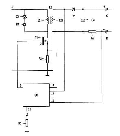
In Fig. 2, the converter and the associated control circuit are shown in
greater
detail. The converter is a flyback converter with a switching element T1
connected in series
with a transformer L2 provided with a primary winding L21 and a secondary
winding L22.
The transformer forms the inductive means. The primary winding L21 is shunted
by a diode
DI which is connected in series with a zener diode Z1 which is oppositely
poled. As a result,
clamping takes place of any peak voltages as a result of a leakage self-
inductance of the
transformer L2 at a level below the breakdown voltage of the switching element
T1. A
current-measuring impedance R3 which is connected in series with the switching
element Tl
is also incorporated in the control circuit. The secondary winding L22 is
connected, via a
diode D2, to an output terminal C and, via a current-measuring impedance R4,
to the output
terminal D. In addition, a buffer capacitor C4 is connected across the series-
combination of
diode D2 and secondary winding L22. The control circuit SC is connected with
an output O
to a control electrode g of the switching element T1. An input I1 of the
control circuit SC is
connected to the current measuring-impedance R3, an input I2 is connected to
the secondary
CA 02343062 2001-03-06
WO 01/05193 PGT/EP00/06Z41
4
winding L22, and an input I3 is connected to the current measuring-impedance
R4. The
control circuit is also provided with an input I4 to~which a temperature-
sensitive element R5,
such as a NTC impedance, is connected. This enables the current through the
semiconductor
light source to be compensated for temperature changes of the light source and
the direct
surroundings thereof. For this purpose, a correction circuit IS32 in the
control circuit is used
to carry out a correction of the signal received at the input I3 by means of
the signal received
at the input I4, as is shown in Fig. 3. In this respect, a diode DS33 in the
path of the
temperature-dependent signal ensures that the correction takes place only if
the temperature-
dependent signal has dropped below a threshold value. The corrected signal is
supplied to
connection pins ISa, ISb of a control-IC IS31, via a combination of a resistor
RS43 and a
capacitor CS33. The resistor RS43 and the capacitor CS33 in combination with
an
operational amplifier present in the control IC ensure that the corrected
signal is integrated.
The size of the resistor RS43 and the capacitor CS33 is preferably chosen to
be such that the
integration time is at least 2.5 times the period T of the alternating voltage
of the supply
source. The control IC is connected through a connection pin I6 to the input
I1, and through a
connection pin I8 to the output O of the control circuit. The input I2 is
connected to a
connection pin I7 of the control IC iS3I. The control IC is preferably a power
factor
correction IC.
The filter means, shown in Fig. 4, comprise a fusistor R1, a varistor R2, a
rectifier bridge
DB1 and a ~t filter consisting of a self-inductance Ll and capacitors C1 and
C2.
In the example described hereinabove, the converter operates in the critical
mode.
In a practical embodiment of the circuit arrangement as described hereinabove,
this circuit arrangement can suitably be connected to a driver having a
voltage in the
conducting state of at least 80 V, 60 Hz and at most 135 V, 60 Hz, and said
circuit
arrangement can also suitably be used to operate a semiconductor light source
comprising a
matrix of 6*3 LEDs, made by Hewlett Packard, having a forward voltage VF,
defined at 2S0
mA and an ambient temperature of 25 °C, between 2 V and 3 V. If the
converter is activated,
the positive pole + of the input filter means carnes a rectified voltage
having an effective
value of at least 80 V and at most 135 V. In conditions where the maximum
permissible
temperature is reached while the supply voltage is minimal, the circuit
arrangement has a
power efficiency of 75%. In comparable conditions, the power efficiency of the
circuit
arrangement in accordance with WO 99/07188 is only 65%.
CA 02343062 2001-03-06
WO 01105193 PCT/EP00/0b241
S
The flyback converter has a 3NB60-type MOSFET, made by SGS-Thompson,
as the switching element. The transformer consists of a ferrite core with a
primary winding of
110 turns of 0.2 mm and a secondary winding having 2 sections of 15 turns of
0.355 mm
each. The control circuit comprises a L6561-type power factor correction IC,
made by SGS-
Thompson, as the control IC, wherein the connection pin ISa corresponds to the
pin INV, ISb
corresponds to COMP, I6 corresponds to CS, I7 corresponds to ZCD, and I8
corresponds to
OUT. The correction circuit IS32 comprises the diode DS33 of the type LL4148.
The
comparator IS33 is a dual comparator of the type LM293, which is also made by
SGS-
Thompson. The current-measuring impedances R3 and R4 are embodied so as to be
a parallel
arrangement of, respectively, 2 and 3 resistors of 1 S2 each. The capacitor C4
is an
electrolytic capacitor having a capacitance of 470 pF. The temperature-
sensitive element RS
is a NTC-resistor of the type B57620C103, made by Siemens.
The capacitors C1 and C2 are filter capacitors having a capacitance of 220 nF
each. The self-
inductance has a size of 2.1 mH. The rectifier bridge DB 1 is built up of 4
diodes, for
example, of the type IN4007.
The converter can suitably be used to reliably operate the LED array in an
ambient temperature range from -40 °C to 70 °C. In the operating
state of the flyback
converter, this converter supplies a minimum current of 540 mA to the
connected LED array.
The converter then withdraws a minimum power of 6 W, which corresponds to a
current
consumption of at least 45 mA. This proves to be sufficient as a holding
current for triac
switches forming part of the supply source. The correction of the
instantaneous current
through the LED array by means of the temperature signal originating from the
NTC resistor
is preferably such that it takes place at an ambient temperature from 25
°C upwards. In this
manner, it is achieved in a very simple manner that, on the one hand,
throughout the ambient
temperature range from -40 °C to +70°C, the holding current
required by the supply source is
withdrawn and, on the other hand, that the quantity of light generated by the
LED array has a
minimum size.
The circuit arrangement described hereinabove can suitably be used to operate
a signal light comprising a light source consisting of a LED array with an
installed power in
the range from 6 W as a minimum to at least 15 W.