Note : Les descriptions sont présentées dans la langue officielle dans laquelle elles ont été soumises.
CA 02483260 2007-11-27
'11Cl-f: OF THE INVENTION
Sl'lJ"1'1'FI2 ('f:)ATING APPARATUS INCLIJDCNCi tON E3i:AM SOURC:E(S),
AND CORRESPONDING METHOD
J0001 l 'T'his iiivention relates to an apparatus for coating a su.bstrate
(e.g., glast
substrate) on both major surfaces,`sides thereof. In particular, this
invention i-elates to
a rncthod and corresponding apparatus for sputtet-ing a coating onto a first
side of the
suhsUate and ion bcana depositing anolher coating onto the othcr sidc of the
substrate.
In other embodiments, this invention relates to a coating apparatus which
sputters a
coating onto a lirst surtace of a substrate passing therethrough and ion beain
mills the
first andror second surface of the substrate in order to reniove glass
therefrom.
BACKGROUND OF THE INVENT1ON
100021 Sputter coated glass articles are known in the art. For example, sec
U.S. 1'atent Nos. 5,770,321, 5,298,048, and 5,403,458, each otf which disclose
coatinbs spultered onto substrates and corresponding tcc.hniclues for the
sante. Sputter
coaled layer systems on glass substrates are t.ypically used tor achieving
solar
management properties (e.g., low eniissivity or low-F.., L1V re[lection,
and/or the like)
in dii7erent types of glass articles including hut not liniited to insulating
glass (IC',)
window units, vehicle windows (e.=., windshields, backlites, sidelites,
sunroofs),
and.!oi- the like.
(0003] Sputter coating rnay be an electric discharge process, often conducted
in a vacutfm c:hamber in the presence of one or rnore gascs. An example
sputtcr
coati.ng apparatus typically includes at least one vacuuin chamber in ttihich
a substrate
is located in a stationary or moving fashion, a power source, an anode, and
one or
1
CA 02483260 2007-11-27
tvore spccifically prepared cathodc tarcel.s of or covered wilh at least one
ntaterial
silicon, r_inc, silver, nickel, chrome. (in., alttminum, other rnateria]s, or
combinations thereol) to be used in creating a laycr(s) on the substrate. When
an
electric potcntial is applied to the cathode target, the oas(es) (e.g., araon,
nitrogen.
oxygen, other gases, or combinations thereol) l`onn(s) a plasma tliat bombards
the
target causing paiticles ot'the coating material to be liberateci or lifted
frorn thc target
itsell: The libcratcd coating material front the target Calls unlo the
underlying
substratc and adlicres thcrcto. When conducted in the presence of a reactive
gas(es), a
reactive product of the coating ntaterial frotn the target and the gas may be
deposited
on the substrate (e.g., in forminb a silicon nitricle layer).
((10041 For oxamplo and witliout limitation, see Fig. 1 which illustrates a
conventional sputter coating apparatus. I he apparatus includes six different
zones
(i.e., zones 1-6) which are separated from one another by curtains or walls
52. Zone I
incluties targets 21-26, zone 2 includes targets 27-29, zone 3 includes
targets.3O-35,
zone 4 inchades targets 36-41, zone 5 includes targets 42-44, and zottc 6
includes
targets 46-50. lhc sptittering targets may he any suitable type of target
including but
not lirnited to planar targets, rotating cylindrical tar6ets, magnetron
targets, andior C-
Mag targets. In the cxample ort'ig. 1, largets 27-29 and 42-44 arc planar
tar;ets,
while targeis ='_ 1-2(i, 30-41, and 45-50 are rotating cylindrical targets. At
lcast one gas
(e.g., argon, nitrogcn, oxygcn, etc.) rnay be utilized in each zone at low
pressure (i.e.,
pressure below atmospheric), while vacuum pumps 51 are provided between zones
in
order to try to i-cducc tttc arnount of crosstalk (i.e., in order to reduce
the atnount of
ras from one /one leaking into an adjacent zorie). A glass substrate is passed
throu.gh
4he sputter coater (e.g., at line speed oi'from 100-300 inches per mintde) in
order to be
coated. Por purposes ofexarnple and without Iinnitatiun, a muili-layered soLar
control
coating can be dcpositcd onto the substrate using this sputt.er coating
apparatus as
explained in more detail in U.S. Patent No. 6:336,999.
10()(151 Other types of sputtering systerns/techniques are disclosed in U.S.
I'atent Nos. 5,968,328, 5,399,252, 5,262,032, i,215,63$, 6,203,677, 6.207,028,
and
5,403,458, ancl 1VO 02!44 37_5.
CA 02483260 2007-11-27
100061 Other example types ot'sputf.ering system are known as ion hcam
assisted sputtering system which utilize an ion hearn(s ) ti) hc;lp liberate
coating
tnaterial lornt a target(s). Sputtering devices of this t}pc may be found, for
example
andwit.hout.litnitation, inanv ofli:S. Patent Nos. 6,197,164, 6,296,741,
orfi,2t4,183.
[00071 I Jnfortunately, each of the a.loresaid sputlerint, devices are
prohlenlatic
in that they can only coat one side of a subsfr.=tte at a time. This is
tuldcsirahlc, at least
#i=om a processing time and capital expenditut-c perspectie=e, in situations
where it is
desired to coat both sides ol'a substrate. Accordingly, it can be seen that
there exists a
need in the art foi- an apparatus which is capable of coatine both sides of a
substrate
withoul. necessarily having to pass the substrate through thc apparatus more
than ane
tinie.
BRIEF SUMMAIZY OF THE INVENTION
[00081 An object of this invention is to provide a coating apparatus capable
of
coating both sides ot'a. subst3=ate.
100091 In certain exaniple enibodinients of this invention, there is provided
a
coalind apparatus which is capable ut'depositing a first coating (single or
multi-
layered) onto a first side of a substrate pas.5ing through the apparatus, and
a second
coating (single oi- niulti-tayered) onto the other or second side of the
substrate passing
through the apparatus. In certain cxattiple enibodiments. the lirst coating
may be
deposited via sputlering from at least one larget while 1hc second coating may
be
deposited via at least one ion beam. In such a marrtrer, it is possible to
coat both sides
o4 the substrate in a single apparatus in an efficient tnanner.' While it is
possible to do
so, it is not necessary to run the substrate through the watinp apparatus
Enore tkzan oite
litne in order to coat both sides of the substrllte.
[0010) In certain example einbodiments of this invontinn, there is provided a
coatine apparatus whicb spullers a coating onto a first side ot a glass
substrate pa:sing
thercthrouph, anci wliich ion beam mills the Jirst an.dlor olhcr ;ide of the
sttbsirate in
orcler to renxrve bl,~ss therefrom.
3
CA 02483260 2007-11-27
100111 In certain example embodiments of this invcntion, there is provided a
coatinb apparatus for forming first and s4cond coatings on a glass substrate,
the
coating apparatus comprising: at least one sputtering target positionexl s<a
as to bc
located at an elevation above a glass substrate passing through the apparatus,
wl.terein
the at least one sputtering target is to be used for sputtering a lint coating
onto a first
side of the glass substrate; at least one ion bcatn source positioned so as to
be locat.ed
at an elevation below thc glass substrate, wherein the at least one ion bcam
source is
to be used to ion beani deposit a second coaling onto a second side of the
glass
substrate opposite the tirst side.
10012j ln other examplc entbodirncnts of this inventicm, there is provided a
ntethod of coating a glass st.ibstrate, the niethod comprising: moving the
glass
substrate through a coating apparatus; attd while the glass substrate is
moving through
the coating appaiatus, siniultaneously sputtering a first coating having at
least one
layer onto a first side of the glass substratc and ion beam dcpositing a
second coating
onto a second side of the substrate that is opposite tltc first side.
100131 In other exainple embodiments of this invention. there is provided a
method ol' li>rming first and second coatings on a glass substrate, the
rnethod
coiuprising: lirrrning a first coating on a first side of the glass substrate;
and while:tt
least part of the firsl: coating is being fotmed on the first side of the
glass substrate, ion
hearn dcposiling a sec.ond coaling onto a second side of the substrate.
1011141 lri olhcr cxample embociirnents of this invention, thcre is provided a
coating deposition apparatus comprising: a dual mode charnbcr for seleclively
reu;iving a rcrnovable ion source module on a('irst side of a rnoving
substr<<te and a
removable sputtering module on a second sidc of the substrate.
100151 In sl.ill I'urthcr embodiments ofthis invention, ttiere is provided a
coating deposition apparatus cotnprisinf; a dual modc chambcr for selectively
reeeiving first and sccond removable iou sources on opposit., sides ol'a
moving
substrate directly across 1i-om one another.
Ll
CA 02483260 2007-11-27
BRIEF DESCRIPTTnN OF THE DRAWI:'VGS
100161 FIGURE t is a schcntatic diagrarn of a con~-cntional sputter coating
apparatu~. -
100171 FICiURt? 2 is a schematic cross sectional diagram of part ofa coating
apparatus according to an example etnbodimettt ofthis invention.
10018] FIGURE 3 is a crciss sectional view of a coated substrate. i.ncluding
coatirtgti urt both sides thcrco(; wttich has [ieen coated using a coating
apparatus
accordirrg to an embodinrent of this invcntion.
[0019] h't(.iUREi 4 is a er-oss sectional view of an insulating glass (IG)
window
unit ntaclc usittg at least the substrate of Fig. 3.
100201 FIGURE 5 is a side cross sectional view of an example, but non-
limiting, ion bcam sourcc which may be used in certain embodinients of this
invctition
[00211 f='1G[IRE 6 is a perspective view of the ion bcam source of Fig. 5.
j0022] F1G[JRE 7 is a sidc plan, partial cross scctional, view illustrating
part
of a coating apparatus according to an example embodiment of ttlis invention,
where a
dual modc chamber is provided.
10023] FTGURE 8 is a side plan, partial cross sectional, view illri_trating
par.f.
ot'a coating apparatus according to the Fig. 7 embodiment, wherein the dual
mode
chamber is shown in a sputter confguration (with sputter tnodule installe(l).
1011241 FTGURTi 9 is a side plan, partial cross sectional, view illu,trating
the
coatina apparatus of Fig. 7, where the duat tnode chamber is shown in an ion
beam
ileposition contiburafion (wittr an ion beam source installed, arid the
sputter module
rcniovcd).
100251 1-'1GI.1RH 10 is a side plan, partial cross sectionai, view
illustrating the
coatinu apparatus of Fit;. 7, whzre the dual rnodc chatnbcr is showtt in a
sittiation
wttere sputter rnodules are installed in both locations, i.e., above and below
the
nzoving substrate.
CA 02483260 2007-11-27
DE I'AILt;D llI;SCRIPTfOIN OF THE INVEN7'lON
(00261 Rcferring, now more parti.cularly to the accompanying drawinas in
which like retcrencc numerals indicatz like parts throughottt the several
views.
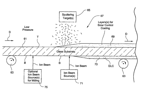
100271 Figure 2 is a perspective view of a coating appaxatus according to an
example L-rnbodinient of this invent.ion. 1'he coating apparatus may include
one or
more sputter coating chamber-s and at least one ion bcarn source used to tnill
and/or
coat the substrate passing thcrethrough. In the Fig. 2 example, glass
substrate 61 is
shown passing through the coating apparatus in direction D. Substrate 61 rnay
be
conveyed through the coating apparatus by a plurality of'rollers 63, or in any
other
suitable manner.
[00281 'T'he coating apparatus includes at least one sputtcring target(s) 65.
C'hc
at least one sputterinb target 65 nlav correspond, for cxarnple and withotit
limitation,
to one or rnore ofsputtcring targcts 21-50 of Fig. 1. In the Fig. 2 example
(and in Pio.
1), the sputtering target(s) 65 is provided at an elevation above the
substrate 61
passing through the wating apparatus so that matcrial 67 to he coated on the
substrate
talls due at least to gavity frotn the target onto [he substrate 61 passing
therebelow in
order to coat the top side T of the substrate 61 tvith sputtetul material.
Sputtering
I.arget(s) 65 may be any suitable typc of sputtering target including but not
limited to a
stationary planar target, a rotating cylindrical targct, antUor a C.-Ulag
targct. For
purposes of example and without limitation, any of the sputtcring targets
and%or
sputtering techniques ol'one or more of U.S. Patent Nos. 5,968,328, 5,399,252,
5162,032, 5,215,638, 6.203,677, 6,207,028, 5,403,458, 5,770,321, 5,298,048,
5,40;,458, 6,197,164, 6,296,741, and/or 6,214,183 niay bc used in order to
cause
target(s) 65 to sputter a coating including at least one iayer onto the
strbstrate 61
passing therebclom,. ()fcourse, the instant invcntion is not so limited, and
any
suitable sputtering technique may also be used, including ion assisted
sputtering. In
such a manner, one or more yputter-ing target(s) cause solar control coating
09 to Ue
spttttered onlo thc uppcr sidc 1' of sttbstrale 61.
[00291 Solar conlrol coating 69, dcpositcd via sputtcring using target(s) 65,
may include one or more layers. Exarnpie solar control coatings Ci9 oE'the
niulti=laver
type are cfiscloscd in U.S. Patcnt Nos. 6,336,999, 5,770,321, 5,40;,458,
5,294,048,
6
CA 02483260 2007-11-27
3.649,359, 3,682.523, 4,716,080, and 4,806,220, and TJ.S.lcrial No.
09i794,224. Of
course, tite instant invcntion is not so limited, and any other type of single
la,ye.r or
multi-laycr coatinS 69 rnay be sputtered onto the top side T of substrate 61
by
target(s) 65. Exantplc solar control coatings 69 may inclnde at least one
infrared (IR)
t-eflccting layer uf or including silver (Ag), gold (Au), nickel-chrome
(NiCr), or any
other suiUtble material. in certain instances, the at least on.; IR reflecting
layer is
metallic or sttbstantiatiy mctalhc and is sanclwiched between at least a pair
of
dielectric layers. 'Che dieiectric layers tnay he of or include silicon
nitride, t.in oxide,
silicon oxynitride, and='or the like. Rach of these laycrs, including the IR
reflecting
layer(s) and diclcctric layer(s) of coating 69, may he deposited via
spttttering,
preferably using a plurality ol'corrzspondittg targets 65 provided above the
moving
substrate 61. For exaniple, a silicon inclusive target(s) nZay be used to
deposit
dielectric layer(s) of silicon nitride of coating 09 in a suitable atmosphere
(e.g., using
gas such as nitrogen and argon), while Ag larget(s) may be used in order 1.0
deposit
A61R rcflecting layer(s) of coating 69 in a suitable atmosphere (e.g., using
Ar gas).
Low pressures are typically used dttring such sputtering of coating 09 (c.g_,
see U.S.
Patcnt Nos. 6,3 36,999, 5,770,321, attd/or 5,298,048), so that the chamber(s)
in which
the target(s) 65 is located is typically maintained at a pressure less than
atmospheric
pressiire.
(0030) Still referring to Fig. 2, the coating apparatus fiurther includes at
least
otte ion bean-t sot,rce(s) 71 which emits an ion beam upwardlytoward the
substrate 61
in order lo coat the bottorn side B of the substrate 61 with coating 73.
Coating 73, ion
bcani deposited on Uhe bottorn side B of substrate 6l , niay be a singlc layer
or may
includc multipie layers in ditTerent emhodiments ofthis invention. In certain
example
embodiments of tlris invention, ion beam deposited coating 73 may be ol'or
inclu<le
diamond-like carbon (DLC) andlor any other suitable material that may be ion
beam
deposited. When coating 73 includcs dianionti-like carbon (DLC), the eoatinc
73 rnay
be of or inelude any of the coal.ings of any of U.S. Patcnt Nos. 6,3 38,901,
6,261,693,
6,284,377, 6,303,225, 5,846,649. 5,637,35;, or any other suitablc coating that
ma_y be
ion beam tleposited onto the substrate. For exarnple, the at least one layer
comprising
DLC rnay iric.lude more shj c,rrhnn --c:uhon bonds than sp~ carbon - carbon
bonds.
Moreover,l.he 1.)1.,(_' may be a special type of U1,C' known as hibhly
rclrahcdral
7
CA 02483260 2007-11-27
amorphous carbon (ta-C) including more sp' carbon - carbon bonds than sp2
car.bon -
carbon boncls. hn eei-tain instances, at least 60 JU of the carbon carbon
bonds in the
ta-C may be spl carbon - carbon bonds, ovcn morc prelei ,tbly at Icatt 70 io.
The DLC
in certain embodiments may be hyilro};entated (e.g., ta-Ca i), anil may have
an
average hardness oi'at least IO (311a, more preferably of at least 21) GPa.
The T)i.C
may be hydrophobic (high contact angle), hvdrophilic (low cimtact angle), or
ncither
in dil"ferent embodiments of this invention.
[0031[ it can he seert that the coating apparatus of the intiiant invention
enables both the top T and bottom B sidcs of inoving glass substrate 61 to be
coated at
the same time as the substrate passes through the coatinb apparatus. One or
more
sputtering tar~ct(s) 65 is/arc uscd to appty a coating 69 to the top side'1'
o1'the
substrate 61, while one or more ion beam sotn'cc(s) 71 is/are usec] to ion
bettm deposit
a coating 73 oitto the bottont sidc B of the substrate 61. In cei-tain example
enlbodiments of tltis invention, the ion bcam source(s) 71 may be in the
sattto
chamber (and thus potentially al appr-oxintately the same low pressure) as one
or more
sputtering target(s) 65 (e.g., in zone 6 oi'Fig. 1). Ilowever, in olficr
emboditnents of
this invention, one or more ion bcant source(s) 71 may be in tliffereat
chambers than
sputtering target(s) 65; in such embodiments a different pressure mav bc: used
to ion
beam deposit than is used to sputter coat. In still hrrther ecnbodiments, a
lirst ion
bcam source 71 may be in the same cha.mber as a first sputtering target(s) 65,
and a
second ion beam sotu=cc 71 and a sccond sputtering target(s) 65 may he in a
different
chnmber or zonc ol'thc coating apparatus at the sonne or a dill'ereiit
pressure. Tn each
of the abovic embodinicnts, the coating apparatus enables one side of'the
glass
stabstrato 61 to be urated with a solar control coating 69 white at the same
time the
other side of the substratc 61 can bc coated with another coatinb 73 such as a
scratch
resistant or protective coating including llL(.' or any other suitrrblo
material.
[0032) Optionally, the coating apparatus may include one o., roore additiona.l
ion beam source(s) 75 provided below the substrate Ior cleaning andlor ion.
beam
mitling the botton.l surt-ac:: ot the substrate. Yor example and withorat
limitation, a
first. ion beam source 75 may he provided (prior to source(s) 71) for ion
hearn milling
at least about 2 A liorn the bottont sicfe 13 of thc k,lass substrate (rnore
prelerably for
R
CA 02483260 2007-11-27
inilling or sltaving off at icast about 5 A of glass from the substrate 61);
and a second
ion bcatn sourcc(s) 7.1 may be provided thereafter for applying coating 73 to
the
rnilled substrate. IL has becn found that the tni.lling may increase scratch
retiistance of
the coating 73 in cerlain instances. It is also possible to provide an ion
beam
source(s) ahove the substrate for ion beam milling a sintifar amuunt ul' glass
lrom the
top side '1' of the substrate 61 before coating 69 is sputtered therconto. For
examplc
milling techniduec'processes~"Ntruclures thatinaybc used in this regard, see
one or
more ofpending U.S. Patent Application Serial Nos. 09l703,709; 10/003,436;
andlor
601340,248.
100331 F;xample coated articles produced by the coating apparatus of Fig. 2
are shown in Fibs. 3-4. The coated article of Fig. 3 includes solar control
coatitlg 69
on one side ol'subsu=ate 61 and protective coating 73 on the other sidc of the
substrate.
Both coatings 69, 73 were applied using a singlc coating apparatus (i.e.,
without
havina to remove the substrate from a lirst coating apparatus and the.n
transpcirt it to a
remote location to another coatitts apparatus). Moreover, the ion bcatn
deposition
process used is such that it is particularly adaptable to application to the
bottom side B
of the substrate 61 (i.c., from ait elevation below the subs(rate, with the
ion beam
bcing directly upwardly toivarrl tbe moving substrate).
100341 Fig. 4 illustratcs the Fig. 3 coated article being used in an
application
such as an insutating glass (t(;) window unit. In Fig. 4, the coated article
of Fig. 3 has
bccn coupletl to another glass substrate 77 via otte or more spacer(s)i,cal(s)
79 to
tirin the EG window unit. In the coated a.trticle of Fig. 4, the spacer(s)
and/or seal(s)
79 space the glass substrates 61, 77 from one ;mothcr so that a space or bap
80 is
provided thei-elaetween. The ;pace or gap 80 may or may not hc filled with a
gas
(e.g., Ar) in cer-tain embodiments of this invention; and may or rnay not be
evacuated
to a pressure less than atmospheric in certain embodiments ofthis invention.
l:n lhe
tG window unit of Fig. 4. it can be appreciated that the solar control coating
69 ou the
interior side of substrate 61 blocks..~rellects at least sonte IR atidior UV
radialion so as
to maintain the interior oI'a building or the like at a more comfortable
t.emhera.[ure;
while the protective coatin 73 on the exterior si(te of substratc 61 may
m,tke the IG
9
CA 02483260 2007-11-27
unit more scratch resi-stant and.'or niherwise durahle than it otherwise would
have
becrt.
[110351 With respect to ion beam sources 71, 75 that may he used in diferent
erobodiments of this invcntion (for ion beani deposition, cleaning and!vr
milling), any
type ofsuitable ion heanl sotuce(s) may he usect. For purposes of'example ancl
without limitation, any ol*the ion beam sourccs disclosed or dcscribed in any
ol't.i.S.
Patent Nos. 6,359,388, 6.303,225, 6,002,208. 6,153,067, 6,338.901, 5,888,593,
or
6,261,693 may be used in accordance Nvith this invention.
10036J H'or purposes of exatnple only, and without limitation, Figures 5-6
illustrate an esample linear or direct ion beam source 125 which may he used
to cican
or mill substrate ! 1 andlor to deposit coatittg 73 ottto the substrate 61
(i.e., thc source
shown may he used as one or both ot'71, 75). Ion beam source 125 includes
gns/powcr inlci 126, racctrack-shapcd anode 127, grounded caihude niabnet
portion
128, magnet poles 129, and insulators 130. A 3-5 kV DC (or AC) power supply
may
be used tiir sotirce 125 in some embodiments. Linear source iun deposition
al.lows for
substantialiy uniforni deposition of a DLC. inclusive layer, or any other
suitable layer,
as to thickness an(lstoichioiY)etry_ Uas(es) andlor ion energy nI ay be
adjusted to make
the coating non-tiniform if dcsired. Ion bcam sonree 125 is based upon a known
gridless ion source design. The linear sotn-ce includes a l.inear sliell
(which is the
cathode and grounded) inside of which lics a cotlcentric ancxie (which is at a
positive
potential). 't'his geometry of cathode-anode and. magnetic tield 1? i gives
rise to a
closed dr-ift. condit.ion. '1'he m:tgncl.ic field configuration further givcs
rise to an anode
Iayer that allows the linear ion beatn source to work absent any electron
ernitter in
certain instances. The iort source can also work in a reactivc; nicxlo (e.g.,
with oxygen
and-or nitrugc:n) in certain cases_ 'I'hc ;otp-ce i.nclu(ics a metal housinp,
witlt a slit in a
shape oC a race track as shown in Figures 5-6. 'I'he hollow housinc is at
cround
potential. The anode electrode is situated within the cathode body (though
etectricall,v
insulatcd) aricl is positioned just below the slit. '1'he anode can be
connected to a
positive potential as high as 3,000 or more volts. 13oth electt-odcs may be
water
cooled in cc.rtain ombodinients.
CA 02483260 2007-11-27
100371 Feedstock ases (e.gõ acetylene. etc.) arc fuithr=ough the cavitv 141
between the anode and cathode. For example, arLon gas niay be used when the
source is used fior cleaning 1ndiir miilitig; wltilc. a hydrocarbon gas (e.g.,
acetylene)
may be us;d when the source(s) is used to deposit a layer(s) of L)I_ C. 1he
linear ion
source may also contain a labyrinth systent that di5trihutes the precursu+-
ga.s evenly
along its lentnh and which allows it to e.xpancf hehWeen the anode-cathode
space
inlernaily. Thc clectrical ertergy then cracks the gas to produce a plasrna
within the
source. The ions are expelled out ancl directed toward the substrate orr which
the
laver(s) is to be ;;rown. The ion beam emanating fi=om the slit is
approximately
unitbrm in the longitudinal direction and may have a Gaussian profile in the
b-ansverse direction. Ion beams rnay be foctised, collim.ated or dittuse in
diftercnt
cmbocliments of this irrvcntion. F"xcnlplary ions 134 directed toward the
tiubstr;tte are
shown in Figure 5. A linear source as lottg as 0.5 to 4 meters may be made and
used,
altltough sourees ol'<iifterent lengths are anticipated in dii3e-rcnt
enibodiment5 ofl.hi.s
invention. r,lcctrun laycr 135 is shown in Figure S and completes the circuit
thereby
enabiing t.he ion be~arn source to funct.ion properly,
(0038] Referring to Figs. 7-9, a dual mocle chamber inay be used in the
apparatus of certain embodiments of this invention. The dual mode cltamber may
he
located, for example, at tlie beginning of a sputter coating apparatus,
proximate a
central area of"a. coating apparatus, andlor at th.e end of'a sputtering
coating apparatus.
In ccrtain entbodiments, the du<tl niocle chtunber may include first and
second
removable deposition modules; where the first deposition modtile is adapted to
be
located above the substrate ancf the second deposition module is adapted to be
located
below the substrate directly or otherwise across fi'om the first module.
[00391 Fig. 7 is a side plan, partial cr'oss sectional, view illustrating at
least
part oFa duai rnode chamber according to an exaniple ot'this invention. "Ihe
chatnber
includes lirst ancl second supporl portions on opposites sides of a moving
glass
substrate which is adapted to inove in direction D. A frmie 200 is provided at
least
partially atxrve anci on a top side of the moving glass substrate, whereas
another fi"ame
202 is provided below and on a bottom side ol'the inoving glass substrate (il
. Rollers
204 are aclapted to support the substrite as it tnoves throuoh the coatirtg
apparatus.
I1
CA 02483260 2007-11-27
Frame 200 is adapted to support a sputter coating module including at least
one
sputtering farget, whereas framc 202 is adapted to suppott an ion source
module
includin6 at least one ion source. Howevcr, f arne 200 (andior 202) may be
used to
support either a sputtering modufe or att ion module in certain alternative
embodiments of this invention. -f'he frames 200 and 202 are shown empty in
Fig. 7,
where rio sptttter coating module or ion source is installed. hrames 200 and
202 may
he located (lirectly across thc substrate 61 from one another in certain
example
emhodiments of this invention. or alternatively niay he located across the
substrate 61
t'rom one another but latcrally spaced ti-om one another in other embodiments
ofthis
invention.
100401 Fig. 8 is side plan, partial cross sectional, views illustrating part
ol'a
coating apparatus accordirig to the Fig. 7 emboditnent, where the dual mode
chaniber
is shown in a sputter configttration (with sputter module installed). In this
par(icular
example configui-ation, Ihe sptrtter module is installeti on top of the glass
substrate,
but the ion snurcu is not installed on the bottom of the substrate. As shown
in fig. 8,
the sputter niodule on the top side of the substrate 61 is supported by frame
200, and
includes sputtering target(s) 209 an(i structure 2) 0 for allowing electrical
sibnals,
gases and thc like to be supplied t(I the targett ot'thc sputterinl; module.
The targets
208 may be of'thc magnetrori dual c-mac) rotating type, the planar type, or
Snv
othet= suitable sputtering target type. Shiolds 21.2 are provided in order to
prevent the
sputtering material fi-om accumulating in undesired locations. Moreover, in
certain
example embodimcnts, shields 212 anti a false wall(s) (not shown) provided
undcr the
substrate in areas between shiclds may fitnction to prevent or reduce drops
(or
inereases) in pressure when there is a gap or space between adjacent
substrates 61
inoving throut;h (he apparatus. Additionally, when the ion source motiule is
not
installed, stipport bearns 214 tnay be provided between rollers tinder the
substrate in
order to support the substrate atid(or the pressure ftlse wall(s) (not shown)
discussed
above. Seals relating to opening(s) in Ji-ame 202 are sealed with gaskets or
the li[cc in
the Fig. 8 cmbodnnent.
10041.1 \Vhen it is desired to change the apparatus ITom asputtering
coniiguration to an ion beam confictu'ation, the sputtering module shown in
Fig. 8
12
CA 02483260 2007-11-27
above the substrate tnay (or may rtot) be retnoved and an ion beant modulc
inscrted as
shown in Pig. 9, In the cxamplc iflustrated in Fig. 9, the sputtering module
of Fig. Y
has been rcrnoved and replaced with at least lateral support beam(s) 220 above
the
substrate. Supports 220 within frame 200 are for supportittg a false wall (nol
shotvn)
locatcd above 1bc substrate: the Rtlse wall, as described above, is tirr
preventireducing
significant pressure changes due to spaces or gaps which occut- between
adjacent
substrates 61 passing t3trough the apparatus during operation. Meanwhile, the
ion
beatn module has been installed below the moving glass substrate as sltown in
F'ig, 9,
where the ion beam. module includes at least one ion source 125 and structure
222 for
pennitting gas(es) and electrical signals to be input to or used by the ion
sources.
When the ion source module ltas been intitalled, the hole in frante 202 f'or
allrrwing
inserting ot'the ion source mcxlule is scaled around the module with gasket(s)
or the
like. 5hiclds 224 arc provided in order to prevent ion source material from
depositing
ou rollers and disrupting operation of thc same. '1'hus, Figs. 9-10
illustratcs the dual
modc chamber in an ion bcam contiguration; wttere the ion beam may bc used to
mill
a surface of the substrate or to deposit a coating thercon. In ccrtain cxample
emboditnents of this invention, certain rollers 204 ma.y be removable in order
to
a.llachm.ent and/or removal of the lower module andior frame.
10042J In certain embodiments of this invention, other sputter coating
chambers (not shown in Figs. 7-9 - but see Figs. 1-2) may be located in the
apparatus
laterally offset from the dual mode chamber anci thus laterally offset from
the Fig. 8-9
ion beam inodule. In such embodimcnts, at least one sputtering tar=gct is used
lor
sputtering a fir,,t coating onto a tirst side of the glass substrate and
siinuftaneously at
least one iori source (see Fig. 9) may be used to mill and/or ion beam deposit
a second
coatin` onto a second side ot'tlte glass substrate opposite the fitst side.
Thus, the ion
hearn source on one sidc of the rnoving substrate and the sputtering
targct(ti) on the
other side of thc substiate nced not bc directly opposite one another (i.c.,
lhcy may be
laterally spaced fr=om one anothcr in certain embodiments).
100431 In other exantple embodiments ol't.liis invention, the dual mode
chamber ofFig. 7 may be contigured so as to simuitaneoualy include two modulcs
above and balnw the substrate respeclively. For example, the dttat niocle
chamber
13
CA 02483260 2007-11-27
may include a.lirst deposition modttle supported by franic 200 above the
movint; -lass
substrate 61 and a second deposition m<xlule supported by &ame 202 located
below
the glass substrate directly across finm the f.irat niodule. In suclt an
example
emboditnent, the first and second eieposition modulcs on opposite sides of fhe
substrate (a) may ho1:h he ion beam deposition modules, (b) tnay both be
sputtering
modules, or (c) one tnay be an ion beam deposition module ancl the other a
sputterittg
nwdulo. For example, and without linailation, hig. 10 illustrates an
embodiment of
the itrstant invention where both frame 200 and frame 202 caeh support a
diflerent
sPuttering niodule so that layer(s) can sitnu3taneously be sputtercd onto both
sides of
the moving substrate 61. hi other situations, the two sputtering modules shown
in
Pib. 10 may each be replaced with an ion source module so that simultaneously
l.irst
and second ion sources may direct ions (for milliiiig or layer deposition) at
the
substrate from opposite sides thereot; respectively. It is noted that when
frames 200
anci 202 each support a nioduie (ion source r odule or sputtering mo(iulc),
the two
niodufes need not be used simultaneotrslv in certain einbodiments of this
invention
aithough bolh are present.
100441 tiVhile the invention has been described in connection with what is
prescritly considered to be the niost practical attd preferred emlx-~d.iment,
it is to be
understood that the invention is not to be limited to the disclosed
etnbodiment, but on.
the contrary, is intend.cd to cover various moditications and ecZuivalent
arrangements
included within tlte spirit and scope o1'the appended claims.
14