Note : Les descriptions sont présentées dans la langue officielle dans laquelle elles ont été soumises.
CA 02817805 2013-05-13
WO 2012/066383
PCT/1B2010/055195
ORTHOGONAL BASIS FUNCTION SET FOR DIGITAL PREDISTORTER
BACKGROUND
The present invention relates generally to techniques for constructing
physical models of
non-linear electronic devices and, more particularly, to methods and apparatus
for
compensating an input signal for distortion introduced to the input signal by
an electronic device.
The design of radio-frequency power amplifiers for communications applications
often
involves a trade-off between linearity and efficiency. Power amplifiers are
typically most
efficient when operated at or near the saturation point. However, the response
of the amplifier
at or near the point of saturation is non-linear. Generally speaking, when
operating in the high-
efficiency range, a power amplifier's response exhibits non-linearities and
memory effects.
One way to improve a power amplifier's efficiency and its overall linearity is
to digitally
predistort the input to the power amplifier to compensate for the distortion
introduced by the
power amplifier. In effect, the input signal is adjusted in anticipation of
the distortion to be
introduced by the power amplifier, so that the output signal is largely free
of distortion products.
Generally, the predistortion is applied to the signal digitally, at baseband
frequencies, i.e.,
before the signal is upconverted to radio frequencies.
These techniques can be quite beneficial in improving the overall performance
of a
transmitter system, in terms of both linearity and efficiency. Furthermore,
these techniques can
be relatively inexpensive, due to the digital implementation of the
predistorter. In fact, with the
availability of these techniques, power amplifiers may be designed in view of
more relaxed
linearity requirements than would otherwise be permissible, thus potentially
reducing the costs
of the overall system.
SUMMARY
The present invention provides a model of an orthogonal basis function set for
use in a
predistortion system. A predistorter applies a distortion function to an input
signal to predistort
the input signal. The distortion function is modeled by a set of orthogonal
basis functions. More
particularly, the output of the predistorter is modeled as the sum of the
output signals from the
orthogonal basis functions weighted by corresponding weighting coefficients.
Techniques are
described for orthogonalizing the basis function output signals depending on
the distribution of
the input signal.
In some exemplary embodiments, a method is provided for compensating for
distortion
of an input signal by an electronic device that operates on the input signal
to produce an output
signal. In one exemplary method a set of model coefficients for a two-
dimensional lattice
prediction model of a basis function set are computed from a set of input
signal samples over a
predetermined sampling interval. The lattice prediction model represents basis
functions in a
predistorter basis function set as different combinations of power basis
functions. A
1
CA 02817805 2013-05-13
WO 2012/066383
PCT/1B2010/055195
corresponding set of predistorter connection coefficients for combining power
basis function
output signals to generate basis function output signals is determined from
the model
coefficients. A set of power basis function output signals is computed from an
input signal and
the set of power basis functions. The set of predistorter connection
coefficients is applied to the
power basis function output signals to produce a set of basis function output
signals, and the
basis function output signals are combined to produce a predistorted input
signal from the input
signal.
In other embodiments of the invention, a predistorter circuit is provided to
compensate
for distortion of an input signal by an electronic device that operates on the
input signal to
produce an output signal. One exemplary predistorter circuit comprises a basis
function
modeling circuit and a predistorter. The basis function modeling circuit
computes a set of model
coefficients for a two-dimensional lattice prediction model of a basis
function set from a set of
input signal samples over a predetermined sampling interval. The lattice
prediction model
represents basis functions in a predistorter basis function set as different
combinations of power
basis functions in a set of power basis functions. The basis function modeling
circuit then
determines, from the set of model coefficients, a corresponding set of
predistorter connection
coefficients for combining power basis function output signals from the power
basis functions to
generate orthogonalized basis function output signals. The model coefficients
computed by the
basis function modeling circuit are used to configure the predistorter. The
predistorter computes
a set of power basis function output signals from an input signal and the set
of power basis
functions. The predistorter then applies the set of predistorter connection
coefficients to the
power basis function output signals to produce a set of basis function output
signals, and
combines the basis function output signals to produce a predistorted input
signal from the input
signal.
In embodiments of the present invention, an orthogonal basis function set is
determined
based on the actual input signal. Therefore, the orthogonal basis function set
derived is
customized to the distribution of the input signal. With the proposed
orthogonal basis function
set, data signals derived from the orthogonal basis function set can be used
to construct a well-
conditioned matrix, which is beneficial for evaluation of the predistorter
weighting coefficients.
BRIEF DESCRIPTION OF THE DRAWINGS
Figure 1 illustrates an indirect model for a predistortion circuit.
Figure 2 illustrates a indirect model for a predistortion circuit.
Figure 3 illustrates a generic distortion model for modeling distortion
introduced by a
predistorter or power amplifier.
Figure 4 illustrates a distortion model without memory for modeling distortion
introduced
by a predistorter or power amplifier.
Figure 5 illustrates an exemplary power basis function set for a distortion
model.
2
CA 02817805 2013-05-13
WO 2012/066383
PCT/1B2010/055195
Figure 6 illustrates an exemplary power basis function set for a distortion
model.
Figure 7 illustrates a distortion model with memory for modeling distortion
introduced by
a predistorter or power amplifier.
Fig. 8 illustrates an exemplary for an orthogonal basis function generator.
Fig. 9 illustrates the structure of a root node for an orthogonal basis
function generator
Fig. 10 illustrates a connecting node for an orthogonal basis function
generator.
Fig. 11 illustrates an exemplary method of predistorting an input signal to a
power
amplifier.
Fig. 12 illustrates an exemplary predistortion circuit for predistorting an
input signal to a
power amplifier.
DETAILED DESCRIPTION
Referring now to the drawings, Figure 1 illustrates a digital predistortion
system 100
configured to compensate for the distortion introduced to a communication
signal by a power
amplifier 120. A power amplifier 120 is typically most efficient when it is
operating in a non-
linear range. However, the non-linear response of a power amplifier 120 causes
out-of-band
emissions and reduces the spectral efficiency in a communication system. A
predistorter 110
may be used to improve power amplifier efficiency and linearity by distorting
the input signal to
the power amplifier 120 to compensate for the non-linear distortion introduced
by the power
amplifier 120. The cascading of a predistorter 110 and power amplifier 120
improves the
linearity of the output signal and thus allows a power amplifier 120 to
operate more efficiently.
Although predistortion is used in the circuits and systems described herein to
linearize the
output of a power amplifier 120, those skilled in the art will appreciate that
the techniques
described are more generally applicable to linearize the output of any type of
non-linear
electronic device.
As seen in Figure 1, an input signal x (n) is input to the predistorter 110.
The
predistorter 110 predistorts the input signal x (n) to compensate for the
distortion introduced by
the power amplifier 120 when the power amplifier 120 is operated in a non-
linear range. The
predistorted input signal z (n) produced by the predistorter 110 is then
applied to the input of
the power amplifier 120. The power amplifier 120 amplifies the predistorted
input signal z (n) to
produce an output signal y (n) . If predistorter 110 is properly designed and
configured, then
the output signal y (n) contains fewer distortion products and out-of-band
emissions than if
power amplifier 120 were used alone.
To compensate for the distortion introduced by power amplifier 120,
predistorter 110
must have a non-linear transfer function that effectively reverses the non-
linear effects of the
power amplifier 120. To properly configure the predistorter 110, an
appropriate model for this
3
CA 02817805 2013-05-13
WO 2012/066383
PCT/1B2010/055195
non-linear transfer function is needed. Two different approaches to deriving
this non-linear
transfer function are possible. The first approach utilizes an indirect-
learning architecture, as
pictured in Figure 1, and the second approach uses the direct-learning
architecture of Figure 2.
In both cases, the signal z (n) input to power amplifier 120 and a scaled
version of the amplifier
output signal y (n) are applied to a distortion modeling circuit 130. The
scaling, illustrated as
attenuator 140 in Figures 1 and 2, reflects the net linear gain G that is
desired from the
combination of predistorter 110 and power amplifier 120. Scaling the output
signal y (n) by the
inverse of G permits the non-linearities introduced by power amplifier 120 to
be analyzed
independently from its gain.
In the indirect-learning architecture of Figure 1, a general structure for a
model of
predistorter 110 is taken as a given, and its coefficients (parameters) are
estimated directly from
the input and outputs of power amplifier 120. The distortion modeling circuit
130 includes a
coefficient evaluation circuit 160 to evaluate the amplifier input signal z
(n) and the amplifier
output signal y (n) I G according to a predetermined non-linear model for the
predistorter to
determine a set of weighting coefficients to be applied by the predistorter
110. This process is
described in further detail below. With this indirect approach, a model for
the power amplifier
120 is not derived. Rather, the non-linear characteristics of power amplifier
120 are learned
indirectly, through the modeling of the predistortion necessary to counteract
the distortion
introduced by power amplifier 120.
In contrast, the direct-learning architecture of Figure 2 directly
characterizes the non-
linear performance of power amplifier 120. The power amplifier includes a
coefficient evaluation
circuit 160 to evaluate the amplifier input signal z (n) and the amplifier
output signal y (n) I G
according to a predetermined non-linear model for the power amplifier 120. The
weighting
coefficients that best fit the power amplifier's non-linear characteristics to
the power amplifier
model in block 120 are then used by a coefficient derivation circuit 170 to
generate weights for
configuring the predistorter 110.
The distortion introduced by the predistorter 110 or power amplifier 120 can
be
represented by a complicated non-linear function, which will be referred to
herein as the
distortion function. One approach to modeling a distortion function, referred
to herein as the
decomposition approach, is to decompose the distortion function into a set of
less complicated
basis functions and compute the output of the distortion function as the
weighted sum of the
basis function outputs. The set of basis function used to model the distortion
function is referred
to herein as the basis function set.
Fig. 3 illustrates a generalized distortion model 200, which may represent the
distortion
introduced by the power amplifier 120 (e.g., as modeled by model coefficient
evaluation unit 160
in the direct learning architecture of Figure 2) or the predistortion transfer
function of predistorter
4
CA 02817805 2013-05-13
WO 2012/066383
PCT/1B2010/055195
(e.g., as modeled by the predistorter model coefficient evaluation unit 160 of
Figure 1). In
either case, the distortion model 200 comprises a structure 210 corresponding
to a desired
basis function set. The model structure 210 includes P taps, where each tap
corresponds to a
basis function. It should be noted that, in some embodiments, multiple taps
may correspond to
the same basis function. The model structure 210 operates on the input signal
x(n) to produce
data signals {u0 (n) , u 1 (n) , . . .0 p _1 (n)} at the respective taps. The
distortion model 200 then
computes a weighted sum of the data signals {up (n) ,ui(n) , . . . u p _1(0}
to obtain a distorted
input signal d (n) . More specifically, the data signals {u0(n),ui(n), . . .0
p_1(n)} are multiplied
by corresponding weighting coefficients {1420 (n) , w 1 (n) , . . . w p _1
(n)} , and the resulting
products are added together to obtain d (n) .
The distortion model shown in Figure 3 can be represented by:
P-1
d (n)= L wP uP (n) Eq. 1
p=0
Equation 1 can be written as a linear equation according to:
d (n) = uT (n)w Eq. 2
where u is a Pxl vector of data signals output by the model structure at time
n and w is a
P x 1 vector of the weighting coefficients applied to respective data signals.
For a given vector u, d (n) is the desired output of the distortion model 200.
In the
direct learning architecture, d (n) is the actual output of power amplifier
120 . In the indirect-
learning architecture, d (n) is the desired output of predistorter 110. The
weighting coefficients
w that best fit the vector u to the desired output d (n) over a period of time
can be learned by
fitting multiple observations of u to the corresponding desired outputs d (n)
. For a set of
observations over N sampling instances, the corresponding linear equations
given in Equation
2 can be expressed as:
U=w = d Eq. 3
where U is a NxP matrix of data signals and d is an Nxl vector corresponding
to the
desired output signal of the distortion model for each of the N sampling
instances. The
columns of the matrix U correspond to the data signals output by respective
taps and the rows
correspond to different sampling instances. Equation 3 can be evaluated
according to well
known techniques (e.g., to minimize a criterion such as a least-square-error
criterion) to find the
weights w that best model the distortion of the amplifier 120 or the
predistorter 110.
5
CA 02817805 2013-05-13
WO 2012/066383
PCT/1B2010/055195
Fig. 4 illustrates an exemplary memoryless distortion model 300 for modeling a
non-
linear system, such as a power amplifier or predistorter. The distortion model
300 comprises K
branches 310, each corresponding to one of K basis functions 320 in a basis
functions set.
For convenience, the k -th branch 310 corresponds to a basis function of the k
-th order. An
input signal sample x (n) passes through each branch 310 and is operated on by
the basis
function 320 to generate a data sample u k (n) , which may also be referred to
more specifically
in this model as the basis function output signal. For each input signal
sample x (n) , the
branches 310 generate a corresponding set of basis function output signals u k
(n) . The basis
function output signal u k (n) for the k -th branch 310 can be expressed as:
u k (n) = f k (x (n)) Eq. 4
where fk (.) denotes a basis function of the k -th order. It may be noted that
the model is
memoryless so the basis function output signal u k (n) depends only on the
current input
sample x (n) . The basis functions output signals {u0 (n) , u 1 (n) , . . . u
K _1 (n)} are multiplied by
corresponding weighing coefficients {1420 (n) , w 1 (n) , . . . w K ¨1 (n)}
and the resulting products are
summed to obtain the distorted input signal d (n) .
Comparing the memoryless distortion model 300 shown in Figure 4 with the
general
distortion model 200 of Figure 3, it may be noted that the number of branches
K in the
memoryless distortion model 300 equals the number of taps P in the general
distortion model
200. It may also be noted that the basis function output signals {u0 (n) , u 1
(n) , . . . u K _1 (n)}
output for a given sampling time instance n in the memoryless model 300
correspond to the
data samples {u0 (n) , u 1 (n) , . . . u p _1(0} in the general distortion
model 200. Thus, the model
of Figure 4 can be viewed as a special case of the distortion model 200 of
Figure 3 where
K = P .
A distortion modeling circuit 130 using the distortion model shown in Figure 4
computes
the weighting coefficients wk (n) for the basis function output signals u k
(n) given x (n) and
d (n) . Accordingly, the weights w that best model the distortion of the
amplifier 120 or the
predistorter 110 can be found in a similar manner to that described above,
e.g., by fitting a
matrix of N observations of the outputs of basis function set to a desired
output signal vector
d. Because distortion model 300 does not account for memory effects, the
accuracy of this
model relative to the actual distortion function of a given power amplifier
120 may be limited.
The basis function set used to model the distortion function may comprise a
set of power
functions used in polynomial models. Fig. 5 illustrates a structure 400, which
may be used to
6
CA 02817805 2013-05-13
WO 2012/066383
PCT/1B2010/055195
implement a set of power basis functions. The structure 400 may be implemented
by hardware
or by a processing circuit. The basis function structure 400 is constructed
from K power basis
functions, denoted f powER,k (.) , where the subscript k indicates a power
basis function of the
k -th order and corresponds to one of the K branches in the distortion model
400. The input
signal sample x (n) passes through each of the power basis functions f powER,k
(.) . For each
input signal sample, the power basis functions generate a corresponding set of
power basis
function output signals f powER,k (x (n)) . When the power basis functions are
used, the data
sample u k (n) can be expressed as:
u k (n) = f POWER,k (x (n)) = x (n)lx (n)lk Eq. 5
The power basis function output signals are then weighted and summed as
previously
described to generate the output signal d (n) of the distortion model.
The basis function set may be designed based on the Voltaire series, which is
widely
used to model non-linear systems. In practical applications, a somewhat
simplified model that
contains fewer terms than the complete Voltaire series can be used to reduce
the computational
complexity without significantly impacting performance. For example, a
polynomial model may
be obtained by omitting all but the power terms and may be implemented as a
multi-branch
model where the power functions are used as a basis function and assigned to
respective
branches 410 of the basis function structure 400.
In some embodiments, an orthogonal basis function set may be derived as the
sum of
power basis function output signals weighted by corresponding scaling
coefficients. In this
case, the data samples output by the basis function set can be expressed by:
k
u k (n) = -f ORTHO, k (x (n)) = L ck,h-f POWER,h (x (n)) Eq. 6
h=0
where fORTHO,k (x (n)) denotes an orthogonal basis function of the k -th
order, the term ck,h
is the weighting factor applied to the h -th order power basis function to
generate the k -th order
orthogonal basis function f
ORTHO,k (x (n)) . An orthogonal basis function set can be
advantageous in many applications, as it can provide better numerical
stability during the matrix
mathematics used to evaluate weighting coefficients for the distortion models.
An orthogonal
basis function set can be constructed as a weighted summation of the power
basis functions.
An orthogonal basis function set can be advantageous in many applications, as
it can provide
better numerical stability during the matrix mathematics used to evaluate
weighting coefficients
for the distortion models.
7
CA 02817805 2013-05-13
WO 2012/066383
PCT/1B2010/055195
Fig. 6 illustrates an exemplary basis function generator 500 to implement an
orthogonal
basis function set. The basis function generator 500 may be implemented by
hardware or by a
processing circuit. The basis function generator 500 comprises a series of
root nodes 510 and
a connecting network 520 comprising a plurality of connecting nodes 530. Each
root node 510
implements a respective power basis function. There is a one-to-one
correspondence between
root nodes 510 and power basis functions. The input signal x(n) passes through
each root
node 510 and the power basis function for each root node 510 generates a
corresponding
power basis function output signal f powER,h(x(n)). The power basis function
output signals
form the input signals to the connecting network 520.
The connecting nodes 530 of the connecting network 520 receive one input and
generate one output. For convenience, the connecting nodes 530 of the basis
function
generator 500 are denoted individually by Nodek,h , where the index h
indicates a
corresponding power basis functions and the index k indicates a corresponding
orthogonal
basis function. The input to Nodek,h is the output of the power basis function
for the h -th root
node 510. Each connecting node 530 multiplies the input by a corresponding
weighting factor
ck,h, referred to herein as the connection coefficient. In the case of
connecting nodes 530
where k is greater than h, the connecting nodes 530 sum the weighted power
basis function
output signals. Each row of the connecting network 520 corresponds to one
orthogonal basis
function. The output of the last (rightmost) connecting node 530 in each row
comprises the
output signal f
ORTHO ,k (x(n)) from one of the orthogonal power basis functions.
An orthogonal basis function set can be designed based on various criteria.
One
design that works well for several common input signal distributions is
derived in Raviv Raich,
Hua Qian, and G. Tong Zhou, "Orthogonal polynomials for power amplifier
modeling and
predistorter design," IEEE Transactions on Vehicular Technology, vol. 53, no.
5, pp.1468-1479,
Sept. 2004.
Memory effects, i.e., the dependence of an output signal on prior states of
the input
signal as well as on the present state, can also be incorporated into a
distortion function. Figure
7 illustrates a non-linear distortion model 600 with memory. The distortion
model 600 comprises
K branches 610. Each branch 610 includes a basis function 620 followed by a
corresponding
memory model 630. The basis function 620, as previously noted, may be one of
the power
basis functions or orthogonal basis functions. In this model 600, the memory
effects
corresponding to each basis function are modeled as a tapped delay line with Q
taps, where Q
is the memory length of the memory model 630. Those skilled in the art will
appreciate that
other memory models, such as a lattice predictor memory model, could also be
used. The
output signal of each branch 610 is a weighted sum of basis function output
signals produced by
8
CA 02817805 2013-05-13
WO 2012/066383
PCT/1B2010/055195
a corresponding basis function over Q sampling time instances, including the
current sampling
time instance and Q-1 previous sampling time instances. For example, if the
basis function for
branch k is fk(.) and the input signal is x(n), then the output of branch k is
a weighted sum
of fk(x(n)), fk(x(n -1)) , fk(x(n -2)), etc. The data signals
{ukQ(n),ukQ i(n),...ukcl q(n),...u(k+1)Q-1(n)} output from the memory model
taps at the
time n are multiplied by corresponding weighting coefficients
{wkQ(n),wkQ 1(n),...wkQ q(n),...,w(k+1)Q-1(n)} and the resulting products are
summed
to produce k branch output signals. The K outputs from the K branches 610 are
then
summed to form the desired distortion signal d (n) .
Comparing the distortion model 600 in Figure 7 with the general model 200 in
Figure 3, it
should be noted that the each branch 610 has Q taps and that there are a total
of KQ taps and
KQ corresponding weights. The total number of taps, KQ, in this model equals
the number of
taps, P, in the general model 200. It should further be noted that the KQ data
signals
{uk.Q (n),ukQ 1(n),...ukc, q(n),...u(k+1)Q-1(n)} correspond to the P data
samples
{u0(n),ui(n),...up_1(n)} output by the model structure 210 in the general
model 200.
A distortion modeling circuit 130 using the distortion model 400 shown in
Figure 5
computes the weighting coefficients {wkQ(n),wkQ i(n),...wkQ q(n)5.==5w(k+1)Q-
1(n)} for
the memory model taps given x(n) and d (n) . Thus, once more, the weights w
(in this case
a lx KQ vector) can be estimated by recording N observations of the outputs of
the KQ
samples, to form a matrix U, and fitting the matrix U to a desired output
signal vector d
according to Equation 3 and a particular optimization criterion. Given an
appropriate basis
function set and a memory model of adequate depth, the resulting distortion
will generally
provide better models of real-world device distortion than a memoryless model.
As suggested in the discussion above, each of the models in Figures 3 -7
includes a
set of data samples u, that can be expressed by:
u T (n)= w = d(n) Eq. 7
1xP Pxl
This is true whether or not the model includes memory. In a memoryless model,
the elements
of uT consist only of the basis function output signals, i.e., each element is
strictly a function of
x(n). In a model with memory, uT also includes elements corresponding to
delayed versions
of the basis function output signals. Thus, some elements of uT may correspond
to a function
9
CA 02817805 2013-05-13
WO 2012/066383
PCT/1B2010/055195
of x(n ¨1) , x(n ¨2), etc. Note that in Equation 7 and as generally used
herein, OT denotes a
transpose, OH denotes a conjugate transpose, P is the number of coefficients
in the model,
the P x 1 vector u(n) denotes all of the data samples in the model at a given
time index n , the
P xlvector w denotes all the coefficients in the distortion model, and d (n)
is the desired
output of the model for time instance n.
For any given time index n, both u(n) and d (n) are known, and Equation 7 is a
linear equation of w. As noted earlier, for observations obtained on N time
indices, the
corresponding linear equations expressed in Equation 7 can be compactly
expressed as:
U = w = d Eq. 8
NxP Pxl Nxl
In Equation 8, U is the input data matrix and d is the desired output vector.
In the indirect-learning architecture of Figure 1, d (n) is the desired output
of
predistorter 110, which ideally has a distortion function that perfectly
compensates for the
distortion introduced by power amplifier 120. Thus, d (n) corresponds to z(n)
, the input to
power amplifier 120, when the indirect-learning architecture is used. The
input signal to the
distortion model, denoted x(n) in Figures 3 ¨ 7, corresponds to the scaled
output of the power
amplifier 120, y(n)1 G. Thus, for any given model structure, samples of the
output from power
amplifier 120 are taken for each of N sampling instances and applied to a set
of basis functions
to produce a matrix U. This matrix U is fitted to the desired output vector d
according to
Equation 8, where d is a vector of samples of the input to power amplifier,
taken at the same
N sampling instances used to form the matrix U.
As discussed earlier, the distortion characteristics for the power amplifier
120 are
modeled directly in the direct-learning architecture, pictured in Figure 2. In
this case, the
"desired" distortion signal d (n) corresponds to the scaled output of power
amplifier 120,
y(n)1 G. The input x(n) to the model corresponds to the input signal of the
power amplifier.
Thus, for any given model structure, samples of the input from power amplifier
120 are taken for
each of N sampling instances and applied to a set of basis functions to
produce a matrix U.
This matrix U is fitted to the desired output vector d according to Equation
8, where d is a
vector of samples of the scaled output from the power amplifier, taken at the
same N sampling
instances used to form the matrix U.
Regardless of the details of the model structure, and regardless of whether
the
indirect-learning architecture or the direct-learning architecture is used, at
the center of the
coefficient evaluation in digital predistorter 110 of Figures 1 and 2 is the
problem of estimating
CA 02817805 2013-05-13
WO 2012/066383
PCT/1B2010/055195
the coefficient vector w based on Equation 8 satisfying a certain criterion.
In order to solve this
estimation problem, inversion of the data matrix U, or UHU , in some form is
required. A well
known measure of sensitivity of a matrix to digital operations, such as matrix
inversion, is the
so-called condition number, which is defined as the ratio of the maximum Eigen
value of a
matrix to its minimum Eigen value. Matrices with condition numbers near 1 are
said to be well-
conditioned.
Because matrix computations can be quite complex, an important goal in the
design
of a distortion model for a power amplifier 120 or a predistorter 110 is to
provide to the
coefficient evaluation algorithm a data matrix UHU that has a relatively small
number of
columns (to reduce the computational complexity of the matrix operations),
that has a condition
number as close to 1 as possible (high numerical stability), and that at the
same time also
models the physical behavior of the power amplifier or predistorter as exactly
as possible, given
a particular optimization criteria. Differences between the distribution of
input signals used to
derive the basis function set for the distortion model and the distribution of
actual data applied to
the predistorter 110 may result in a data matrix UHU with a large condition
number.
This added instability is reflected in a significant increase, sometimes as
much as by
a factor of 106, of the condition number of the data matrix that has to be
inverted in the
coefficient evaluation process. This problem can be quite serious in an
adaptive digital pre-
distortion system with memory, as the parameters in such a system have to be
adapted "on the
fly" to track the distortion characteristics of the power amplifier over time.
One factor
contributing to these high condition numbers is a mismatch between the signal
distribution of the
real-world signals and the signal distributions of the signals used to derive
the orthogonal basis
function set. Therefore, an orthogonal basis function set developed in view of
a particular
expected input signal distribution is unable to provide orthogonalized basis
function outputs from
a direct application to real signals.
Fig. 8 illustrates an orthogonal basis function generator 700 for implementing
an
orthogonal basis function set. As described in more detail below, the
orthogonal basis function
generator 700 can be used to generate a set of orthogonalized basis function
output signals
based on the distribution of the input signals. Consequently, the matrix UHU
formed from the
basis function output signals will have a low condition number that makes the
matrix UHU
more suitable for coefficient evaluation.
The orthogonal basis function generator 700 comprises a plurality of root
nodes 710 and
a connecting network 720 comprising a plurality of connecting nodes 730. The
nodes 710, 730
of the orthogonal basis function generator 700 are denoted by the notation
Nodek,h , where the
indices k and h denote rows and columns in Fig. 8. The input to the orthogonal
basis function
generator 700 is assumed to be a finite sequence of N input signal samples
rather than a
11
CA 02817805 2013-05-13
WO 2012/066383
PCT/1B2010/055195
continuous stream. Because the input to the orthogonal basis function
generator 700 is a finite
sequence, a two-dimensional lattice structure is used to orthogonalize the
basis function output
signals as hereinafter described.
Each node 710, 730 in the orthogonal basis function generator 700 generates
forward
and backward prediction errors, denoted respectively by Ali (n) and b kh (n) ,
for each sample
time instance n. The forward and backward prediction errors Ail (n) and b kh
(n) are then
normalized to generate normalized forward and backward prediction errors,
denoted
respectively by 7 k,h (n) and kh(n) . In the case of the root nodes 710, the
normalized
forward prediction error jo ,h (n) equals the normalized backward prediction
error kh (n) . As
will be described in greater detail below, the only input to the root nodes
710 during a sampling
time instance is a single input signal sample x (n) . The same input signal
sample x (n) is
applied to each root node 710. The connecting nodes 730 have two inputs each,
which are the
normalized forward prediction error lic-1,h (n) from Nodek_Lh and the
normalized backward
prediction error Fk_i,h+i(n) from Nodek_i,h+1(n) = The normalized backward
prediction error
F k ,0 (n) from Nodek,0 , which denotes a node 710, 730 in the rightmost
column of Fig. 8, is the
output of the k -th order orthogonal basis function which may be expressed as:
1orth,k-1 (x (n)) = b k ¨1,0 (n) Eq. 9
It should be noted that the outputs of the orthogonal basis functions given by
Eq. 9 are a
function only of the current input sample x (n) and do not depend on previous
or future input
signal samples.
Fig. 9 illustrates the structure of a root node 710. The root nodes 710 are
denoted by
the notation Nodeo , i.e. nodes where k equals 0.. The root nodes 710 each
comprise a
respective power basis function 740 and a normalization circuit 750. The power
basis function
740 in each root node 710 operates on the input signal sample x (n) to
generate the forward
and backward prediction errors for the root node 710. That is, the forward and
backward
prediction errors Ail (n) and b kh (n) for the root nodes 710 equal the power
basis function
output signal fpoweo (x (n)) . The normalization circuit 750 normalizes to a
predetermined
value the power basis function output signal fpoweo (x (n)) to generate
normalized forward
and backward prediction errors Ah (n) and kh (n) for the root node 710. More
particularly,
the normalization circuit 750 multiplies the power basis function output
signal fpoweo (x (n))
12
CA 02817805 2013-05-13
WO 2012/066383
PCT/1B2010/055195
by a corresponding normalization factor ak ji to generate normalized forward
and backward
prediction errors Ah(n) and kh(n), which may be expressed as:
bo(n)= aobo(n)= aofpower,h (x(n)) Eq. 10
f0,h(n)= a0,hf0,h(n)= a0,hfpower,h (x(n)) Eq. 11
The normalization factor ao applied by each root node 710 is a function of the
variance of the
input signal x(n) over a predetermined time period and the power basis
function as will be
describe below.
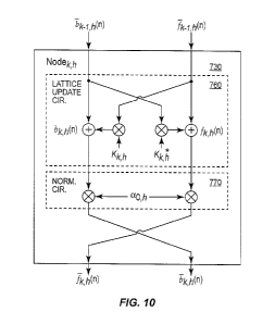
Fig. 10 illustrates the structure of a connecting node 730 of the connecting
network 720.
Each connecting node 730 in the connecting network 720 comprises a lattice
update circuit 760
and a normalization circuit 770. As previously noted, the inputs to a given
connecting node 730
comprise the normalized forward prediction error jk-1,h (n) from Nodek_Lh and
the
normalized backward prediction error Fk -1,h+1 (n) from Nodek_i,h+i . The
outputs of the
connecting nodes 730 are revised estimates of the normalized forward and
backward prediction
errors, denoted respectively by Ah(n) and bkh(n). In the case of the nodes
along the
diagonal where h = K - k -1 , the normalized forward prediction error Ah(n) is
not used and
the related circuits could therefore be omitted.
The lattice update circuit 760 scales the normalized forward and backward
prediction
errors A-1,h (n) and bk_i,h+i(n) input to the connecting node 730 by a
corresponding
_
reflection coefficient Ick,h . More particularly, the forward prediction error
A-1,h (n) input to the
connecting node 730 is multiplied by the reflection coefficient Ick,h and the
resulting product is
added to the backward prediction error Fk_i,h+i (n) to generate a revised
backward prediction
error bkh(n). Similarly, the backward prediction error Fk_im i (n) input to
the connecting
*
node 730 is multiplied by the conjugate of the reflection coefficient, denoted
K. k,h, and the
resulting product is added to the forward prediction error jk-1,h (n) to
generate a new forward
prediction error Ah(n). For purposes of this application, the reflection
coefficient Ick,h and its
*
conjugate K. ic,h are considered to be the connection coefficients for the
lattice predictor model.
The revised forward and backward prediction errors may be expressed by:
fk,h(n)= fk-1,h(n)+ ick,hbk-1,h+1(n) Eq. 12
bk,h(n)=bk-1,h+1(n)+ ick,hfk-1,h(n) Eq. 13
13
CA 02817805 2013-05-13
WO 2012/066383
PCT/1B2010/055195
The normalization circuit 770 multiplies the revised forward and backward
prediction errors
fk,h(n) and bkh(n) by a corresponding normalization factor ak,h to generate
new
normalized forward and backward prediction errors Ah(n) and F,k,h(n) , which
may be
expressed as:
fk,h(n)= ak,hfk,h(n) Eq. 14
bk,h(n)=ak,hbk,h(n) Eq.
15
The normalization introduced into the nodes 710, 730 is used to enforce wide
sense
stationary. Fora given node Nodek,h , where ClicK-1 and the
normalization factor ak,h is given by:
1
1 -
ak,h=(var(bk,h(n))) 2 a = E (bk,h(n)¨nik,h)(bk,h(n)¨nik,h)* a Eq. 16
where the term var denotes variance, the term E denotes expected value, and
the term mk,h
denotes the mean of the backward prediction error bkh(n) and equals zero when
the input
signal x(n) has zero mean. It has been previously noted that, in the case of
the root nodes,
the backward prediction error equals the power basis function output signal.
The term a is the
desired square root of variation and is normally static. For most
applications, the desired
variance may be set equal to 1 to get good performance.
The reflection coefficients ick,h and lc* k,h applied by the connecting nodes
730 are
evaluated based on an input sequence of N samples {x(0),x(1),===,x(N-1)} . The
reflection coefficient Ick,h for the connecting nodes 630 where 0 hK ¨k ¨1 is
given by:
2V N-1 *
= bk¨lh+1(n)fk-1,h(n)
ickh
n=0
,
\12 1, õ12 Eq.
17
Ln=0 LIJk-1,h 111/1 +114-1,h+1)1 ]
where the superscript * denotes conjugation.
The lattice predictor model for the orthogonal basis function generator 700
described
above could be used to implement a predistorter 110 as shown in Figures 1 and
2. In this case,
the normalization factors ak,h for each node 710, 730 and the reflection
coefficients ick,h for
the connecting nodes 730 need to be evaluated. If the input signal x(n) is
wide sense
stationary, the reflection coefficients ick,h , Kk,h and normalization factors
ak,h could be
evaluated based on a sequence of N consecutive input samples x(n). The
predistorter 110
14
CA 02817805 2013-05-13
WO 2012/066383
PCT/1B2010/055195
could then be statically configured with the computed normalization factors
ak,h and reflection
coefficients ick,h . If the input signal is not wide sense stationary, the
normalization factors
ak,h and reflection coefficients ick,h may need to be reevaluated
periodically. In this case, the
statistics of the input signal may be monitored and the connection
coefficients may be
periodically updated. The statistics of the input signal may remain static for
periods of time and
then change. Thus, once the connection coefficients are computed, the
connection coefficients
may be used to predistorter the input signal until the statistics of the input
signal indicate the
need for new connection coefficients. As noted previously, the reflection
coefficients ick,h in
lattice model of the predistorter 110 are considered to be connecting
coefficients.
Because the basis function set, lattice update function, and normalization
function are all
linear, the predistorter 110 could equivalently be implemented by the
orthogonal basis function
*
generator 500 shown in Fig. 6. In this case, the reflection coefficients
ick,h, 1( k,h and
normalization factors ak,h computed based on the lattice predictor model of
the basis function
set could be used to derive the connection coefficients for the connecting
nodes 530 in the
network structure 500.
Fig. 11 illustrates an exemplary method 800 of predistorting an input signal
to an
electronic device to compensate for distortion introduced by the electronic
device. A finite
sequence of input signal samples is applied to a coefficient evaluation
circuit that determines
the connection coefficients for an orthogonal basis function set modeled as
shown in Figs. 6 or
8. The coefficient evaluation circuit computes a set of model coefficients for
a two-dimensional
lattice prediction model of a basis function set based on the input signal
samples (block 810).
The lattice prediction model represents the basis functions in the
predistorter basis function set
as different combinations of power basis functions as shown in Fig. 10. In one
embodiment, the
model coefficients comprise the reflection coefficients for the lattice
predictor model of the
orthogonal basis function set as shown in Fig. 10. The model coefficients may
be computed
according to Equation 17 .The coefficient evaluation circuit then determines,
from the set of
model coefficients, a corresponding set of predistorter connection
coefficients for combining
power basis function output signals from the power basis functions to generate
orthogonal basis
function output signals (block 820). In one exemplary embodiment, the
predistorter 110 is
based on the same lattice prediction model for the basis function set as the
coefficient
evaluation circuit. In this case, the model coefficients (e.g., reflection
coefficients) can be used
as predistorter connection coefficients because the two models are the same.
In this case, it
would also be necessary to periodically evaluate the normalization factor for
each connecting
node 530. In other embodiments of the invention, the predistorter 110 may
implement an
equivalent model for the basis function set as shown in Fig. 6 where the
orthogonal basis
CA 02817805 2013-05-13
WO 2012/066383
PCT/1B2010/055195
functions are modeled as sums of power basis function output signals weighted
by respective
connection coefficients. In this case, the predistorter connection
coefficients may be computed
from the model coefficients and the corresponding normalization factors
derived for the lattice
prediction model. The predistorter 110 is then configured with the connection
coefficients
computed at 820.
As previously noted, the predistorter 110 is used to predistort an input
signal sample to
compensate for the distortion introduced by a power amplifier or other non-
linear device. An
input signal is applied to the pre-configured predistorter 110. The
predistorter 110 computes a
set of power basis function output signals by applying a set of power basis
functions to the input
signal sample, (block 830). The set of predistorter connection coefficients
computed in block
820 are then applied to the power basis function output signals to produce a
set of orthogonal
basis function output signals (block 840). The basis function output signals,
in turn, are
weighted by respective weighting coefficients and combined to generate a
predistorted input
signal for input to a power amplifier (block 850). It should be noted that the
input signal sample
being predistorted in blocks 830 through 850 need not be the same as the one
used to derive
the connection coefficients in blocks 810 and 820. In practice, the statistics
of the input signal
may be monitored and the connection coefficients may be periodically updated.
The statistics of
the input signal may remain static for periods of time and then change. Thus,
once the
connection coefficients are computed, the connection coefficients may be used
to predistort the
input signal until the statistics of the input signal indicate the need for
new connection
coefficients.
Fig. 12 illustrates an exemplary predistortion circuit 900 according to one
exemplary
embodiment. The predistortion circuit 900 comprises a predistorter 910
implementing a basis
function structure as shown in Figs. 4 or 8, a power amplifier 940, distortion
modeling circuit
950, and basis function modeling circuit 960. An input signal x (n) is applied
to a predistorter
910. The predistorter 910 comprises a basis function generator 920 and a
combiner 930. The
basis function generator produces a set of orthogonal basis function output
signals from the
input signal sample using one of the models shown in Figures 4 and 8. The
combiner 930 sums
the basis function output signals weighted by respective weighting
coefficients to produce the
predistorted input signal z (n) The power amplifier 940 amplifies the
predistorted input signal
z (n) to produce an output signal y (n) . The power amplifier may be operated
in a non-linear
mode to efficiently amplify the predistorted input signal. The predistortion
applied by the
predistorter compensates for the distortion introduced by the power amplifier
so that the
cascade of the predistorter and power amplifier is nearly linear.
The distortion modeling circuit 950 determines the weighting coefficients
applied by the
combiner 930 to the basis function output signals to produce the predistorted
signal z (n) . The
16
CA 02817805 2013-05-13
WO 2012/066383
PCT/1B2010/055195
distortion modeling circuit 950 may use well-known techniques described above
to compute the
weighting coefficients by modeling the distortion of the power amplifier or
predistorter.
Generally, the distortion modeling circuit computes a set of weighting
coefficients using a
distortion model for the power amplifier (direct approach) or predistorter
(indirect approach) that
best fits the predistorted signal z (n) to the output signal y (n) . Co-
pending applications filed
concurrently with this application entitled Joint Process Estimator with
Variable Tap Delay Line
for use in Power Amplifier Digital Predistortion, Configurable Basis-Function
Generation for
Nonlinear Modeling, and Non-Linear Model with Tap Output Normalization,
describe additional
techniques for computing weighting coefficients. These co-pending applications
are
incorporated herein in their entirety by reference.
As noted above, the predistorter 910 uses one of the models shown in Figures 4
and 8
to produce the orthogonal basis function output signals. In either case, the
basis function
modeling circuit 960 computes the connection coefficients to be applied by the
basis function
model from a sample sequence of the input signal x (n) . Thus, the basis
function set applied to
the input signal by the predistorter 910 is dependent on the distribution of
the input signal. By
matching the orthogonal basis function set to the distribution of the input
signal, the condition
number of the matrix UHU produced from the orthogonal basis function set is
significantly
lowered. The orthogonal basis function set can be implemented using the
structure shown in
either Fig. 8 or Fig. 8. The structure shown in Fig. 6 is backward compatible
with the power
basis function set.
The basis function modeling circuit evaluates an orthogonal basis function set
based on
the actual input signal. Therefore, the orthogonal basis function set it
derives is customized to
the distribution of the input signal. With the proposed orthogonal basis
function set, the
condition number of the data matrix is significantly lowered. For example,
simulation has shown
a reduction of the condition number from about 108 to about 1.0018. The basis
function
modeling circuit can be implemented using the orthogonal basis function model
shown in Figure
6, which is a general structure and backward compatible with the power basis
function sets.
The present invention may, of course, be carried out in other specific ways
than those
herein set forth without departing from the scope and essential
characteristics of the invention.
The present embodiments are, therefore, to be considered in all respects as
illustrative and not
restrictive, and all changes coming within the meaning and equivalency range
of the appended
claims are intended to be embraced therein.
17