Note : Les descriptions sont présentées dans la langue officielle dans laquelle elles ont été soumises.
CA 02978396 2017-08-31
DESCRIPTION
TITLE OF INVENTION
DATA RECEIVING APPARATUS
TECHNICAL FIELD
The present invention relates to an apparatus for receiving data transmitted
at a
plurality of transmission rates (multiple rates).
BACKGROUND ART
A passive optical network (PON) system is a kind of optical communications
system. A PON system includes an optical line terminal (OLT), one or more
optical
network units (ONUs), an optical fiber to transmit an optical signal, and an
optical
splitter to allow the optical fiber to branch. The OLT is connected to the
ONUs with
the optical fiber and the optical splitter. The optical splitter is installed
between the
OLT and the ONUs. In this way, a plurality of optical network units can be
connected
to one optical line terminal.
The IEEE 802.3 standard prescribes the GE-PON and the 10G-EPON as
standards of the PON. One of the differences between the GE-PON and the 10G-
EPON is a transmission rate of data. The transmission rate of the GE-PON is
1.25
Gbps (bit per second). The transmission rate of the 10G-EPON is 10.3125 Gbps.
One PON system may include both the GE-PON and the 10G-EPON. An
example of such a system is disclosed in Japanese Patent Laying-Open No. 2010-
252044 (PTD 1).
CITATION LIST
PATENT DOCUMENT
PTD 1: Japanese Patent Laying-Open No. 2010-252044
SUMMARY OF INVENTION
TECHNICAL PROBLEM
Japanese Patent Laying-Open No. 2010-252044 does not disclose a
configuration for an OLT to receive data sent at a plurality of different
transmission
- 1 -
CA 02978396 2017-08-31
rates (multiple rates). An object of the present invention is to provide a
configuration
for receiving transmission data at multiple rates where one rate is not
necessarily a
multiple of another.
SOLUTION TO PROBLEM
A data receiving apparatus according to an embodiment of the present invention
includes: a data receiving circuit including a first receiving unit configured
to receive a
first data signal transmitted at a first rate, and a second receiving unit
configured to
receive a second data signal transmitted at a second rate different from the
first rate;
and a path switch including first and second input terminals and first and
second output
terminals, the path switch being configured to define a path of signal between
at least
one of the first and second input terminals and at least one of the first and
second
output terminals to route an input data signal to at least one of the first
receiving unit
and the second receiving unit.
ADVANTAGEOUS EFFECTS OF INVENTION
According to the above, a configuration for receiving transmission data at
multiple rates where one rate is not necessarily a multiple of another can be
implemented.
BRIEF DESCRIPTION OF DRAWINGS
Fig. 1 is a schematic diagram showing an example configuration of an optical
communications system according to an embodiment of the present invention.
Fig. 2 is a block diagram showing a part of a configuration of an OLT
according
to an embodiment of the present invention.
Fig. 3 is a block diagram showing a first example configuration of an optical
transceiver.
Fig. 4 is a block diagram showing a second example configuration of an optical
transceiver.
Fig. 5 is a diagram showing a path in a cross point switch defined
corresponding
to the first example configuration of an optical transceiver.
Fig. 6 is a diagram showing a first path in a cross point switch defined
- 2 -
CA 02978396 2017-08-31
corresponding to the second example configuration of an optical transceiver.
Fig. 7 is a diagram showing a second path in a cross point switch defined
corresponding to the second example configuration of an optical transceiver.
Fig. 8 is a diagram illustrating routing of a signal by a cross point switch
according to another embodiment of the present invention.
Fig. 9 is a diagram illustrating routing of a signal by a cross point switch
according to still another embodiment of the present invention.
Fig. 10 is a diagram showing a configuration of a WDM (wavelength division
multiplex) optical communications system according to an embodiment of the
present
invention.
DESCRIPTION OF EMBODIMENTS
Description of Embodiments of Invention
First, embodiments of the present invention are enumerated. In the following
description, the term "terminal" can be replaced with the term "port". The
terms
"first" and "second" are used to distinguish a plurality of identical or
similar
components from one another and are not intended to specify the order of the
components.
(1) A data receiving apparatus according to an embodiment of the present
invention includes: a data receiving circuit including a first receiving unit
configured to
receive a first data signal transmitted at a first rate, and a second
receiving unit
configured to receive a second data signal transmitted at a second rate
different from
the first rate; and a path switch including first and second input terminals
and first and
second output terminals, the path switch being configured to define a path of
signal
between at least one of the first and second input terminals and at least one
of the first
and second output terminals to route an input data signal to at least one of
the first
receiving unit and the second receiving unit.
According to such a configuration, the path switch can sort data signals into
the
first receiving unit and the second receiving unit. Thus, a configuration for
receiving
transmission data at multiple rates where one rate is not necessarily a
multiple of
- 3 -
CA 02978396 2017-08-31
another can be implemented.
(2) Preferably, the data receiving apparatus further includes a control
circuit
configured to control the path in the path switch. The first output terminal
is a
terminal to output the first data signal to the first receiving unit. The
second output
terminal is a terminal to output the second data signal to the second
receiving unit.
The control circuit is configured to control the path in the path switch in
accordance
with a mode selected from among a first mode, a second mode, and a third mode.
The
first mode is a mode in which the first input terminal and the first output
terminal are
connected to each other and in which the second input terminal and the second
output
terminal are connected to each other. The second mode is a mode in which any
one of
the first and second input terminals is connected to the first and second
output terminals
switchably. The third mode is a mode in which any one of the first and second
input
terminals is connected to the first and second output terminals.
According to such a configuration, the control circuit can appropriately
control
a path within the path switch in accordance with a data signal input to at
least one of
the first and second input terminals of the path switch.
(3) Preferably, the path in the path switch is set so that a terminal, among
the
first and second input terminals, receiving input of the data signal is
connected to the
first and second output terminals. The data receiving apparatus further
includes a rate
determining unit configured to determine a rate of transmission of the data
signal based
on whether or not the data signal has been successfully received by at least
one of the
first receiving unit and the second receiving unit.
According to such a configuration, a path within the path switch can be
appropriately controlled based on a determination result from the rate
determining unit.
(4) Preferably, the path in the path switch is controlled so that a terminal,
among the first and second input terminals, receiving input of the data signal
is
connected to the first and second output terminals switchably. The data
receiving
apparatus further includes a rate determining unit configured to determine a
rate of
transmission of the data signal based on whether or not the data signal has
been
- 4 -
CA 02978396 2017-08-31
successfully received by at least one of the first receiving unit and the
second receiving
unit.
According to such a configuration, a path within the path switch can be
appropriately controlled based on a determination result from the rate
determining unit.
(5) Preferably, the data receiving apparatus is included in an optical line
terminal of an optical communications system.
According to such a configuration, an OLT for appropriately receiving
transmission data at multiple rates where one rate is not necessarily a
multiple of
another can be implemented.
Details of Embodiments of Invention
Embodiments of the present invention are described below with reference to the
drawings. In the drawings, identical or corresponding components are
identically
denoted and explanations for such components are not repeated.
Fig. 1 is a schematic diagram showing an example configuration of an optical
communications system 1 according to an embodiment of the present invention.
With
reference to Fig. 1, optical communications system 1 includes an optical line
terminal 2,
a plurality of optical network units 3a, 3b, 3c, ..., a trunk line optical
fiber 4a, a
plurality of leaf line optical fibers 4b, an optical coupler 5, and an optical
signal
repeater 7. The optical line terminal is hereinafter referred to as an "OLT",
and the
optical network units are hereinafter referred to as "ONUs". Each of ONUs 3a,
3b, 3c
is installed in a subscriber's place. Trunk line optical fiber 4a is connected
to OLT 2.
Each leaf line optical fiber 4b is connected to a corresponding ONU. Optical
coupler
5 connects trunk line optical fiber 4a with a plurality of leaf line optical
fibers 4b.
Optical signal repeater 7 is disposed in the middle of trunk line optical
fiber 4a.
Optical communications system 1 forms a system including the GE-PUN and
the 10G-EPON. The GE-PUN has a communication speed (transmission rate) of 1.25
Gbps. The 10G-EPON has a communication speed (transmission rate) of 10.3125
Gbps. A signal at a transmission rate of 1.25 Gbps is hereinafter also
referred to as a
"1G signal". On the other hand, a signal at a transmission rate of 10.3125
Gbps is
- 5 -
CA 02978396 2017-08-31
hereinafter also referred to as a "100 signal".
OLT 2 can receive both an upstream signal of the GE-PON and an upstream
signal of the 10G-EPON. That is, OLT 2 is configured to be capable of
receiving data
sent at a plurality of different rates. Further, OLT 2 can send both a
downstream
signal of the GE-PON and a downstream signal of the 10G-EPON.
Each of ONUs 3a, 3b, 3c is a unit for a subscriber to enjoy an optical network
service. Each ONU sends an upstream signal. The upstream signal has a
communication speed of either 1.25 Gbps or 10.3125 Gbps. Each ONU receives a
downstream signal. The downstream signal has a communication speed of either
1.25
Gbps or 10.3125 Gbps. As shown in Fig. 1, communication speeds of upstream and
downstream signals of each ONU are any one of four combinations.
Optical coupler 5 is connected to trunk line optical fiber 4a and a plurality
of
leaf line optical fibers 4b. Optical coupler 5 distributes an optical signal
sent through
trunk line optical fiber 4a to a plurality of leaf line optical fibers 4b.
Further, optical
coupler 5 multiplexes optical signals sent from a plurality of leaf line
optical fibers 4b
and delivers them to trunk line optical fiber 4a. Optical coupler 5 can
include, for
example, an optical star coupler.
OLT 2 and each of ONUs 3a, 3b, 3c communicate with each other in units of
variable-length frames.
Now, the sending of an upstream signal by each ONU is described. A terminal
device of each subscriber's place sends data. The data is converted into an
optical
burst signal by an ONU. The optical burst signal is composed of bits. If the
sending
rate of the ONU conforms to the GE-PON, the bit transmission rate is 1.25
Gbps. On
the other hand, if the sending rate of the ONU conforms to the 10G-EPON, the
bit
transmission rate is 10.3125 Gbps.
ONU 3a sends an optical burst signal 6a. ONU 3b sends an optical burst
signal 6b. ONU 3c sends an optical burst signal 6c. The transmission rates of
optical burst signals 6a, 6b are both 1.25 Gbps. The transmission rate of
optical burst
signal 6c is 10.3125 Gbps.
- 6 -
CA 02978396 2017-08-31
Optical coupler 5 multiplexes optical burst signals 6a, 6b, 6c and outputs an
optical signal to trunk line optical fiber 4a. The optical signal from optical
coupler 5
is sent to OLT 2 through optical signal repeater 7.
OLT 2 sends a control frame to each of ONUs 3a, 3b, 3c. The control frame
allocates a time window to each of ONUs 3a, 3b, 3c for sending an upstream
optical
signal. Therefore, optical burst signals 6a-6c do not conflict with one
another on a
time axis. OLT 2 obtains a transmission rate and a reception timing of an
optical burst
signal to be received by allocating a time window to each of ONUs 3a, 3b, 3c.
Optical signal repeater 7 is a device to repeat an optical signal. Optical
signal
repeater 7 can increase a transmission distance of an optical signal, i.e., a
distance
between the OLT and the ONUs.
Upon receiving an optical signal, optical signal repeater 7 converts the
optical
signal into an electrical signal. Optical signal repeater 7 performs various
kinds of
processing to the electrical signal. Optical signal repeater 7 then converts
the
electrical signal into an optical signal and delivers the optical signal.
Upon receiving an optical signal, optical signal repeater 7 shapes the
waveform
of the signal. Further, optical signal repeater 7 equalizes strengths of a
plurality of
optical signals to be output. Optical burst signals 6'a, 6'b, 6'c are
substantially the
same in strength. Optical signal repeater 7 generates optical signals to be
output based
on a plurality of optical burst signals so that signals corresponding to a
plurality of
pieces of data are the same in level.
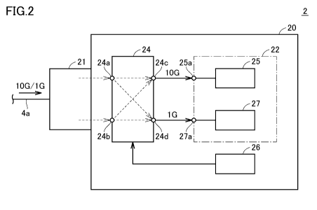
Fig. 2 is a block diagram showing a part of a configuration of OLT 2 according
to an embodiment of the present invention. A part of the configuration of OLT
2
responsible for reception of an optical signal is shown in Fig. 2. That is, a
data
receiving apparatus according to an embodiment of the present invention is
disclosed in
Fig. 2. OLT 2 includes a host board 20 and an optical transceiver 21. Host
board 20
includes a receiving circuit 22, a cross point switch (path switch) 24, and a
switch
control circuit 26.
Receiving circuit 22 receives both a data signal (1G signal) transmitted at
1.25
- 7 -
CA 02978396 2017-08-31
Gbps and a data signal (10G signal) transmitted at 10.3125 Gbps. Receiving
circuit
22 includes an input terminal 25a, an input terminal 27a, a 10G signal
receiving unit 25,
and a 1G signal receiving unit 27. Input terminal 25a receives a 10G signal.
Input
terminal 27a receives a 1G signal. 10G signal receiving unit 25 receives a 10G
signal
through input terminal 25a. 1G signal receiving unit 27 receives a 1G signal
through
input terminal 27a.
10G signal receiving unit 25 is a dedicated circuit for the 10G-EPON. 1G
signal receiving unit 27 is a dedicated circuit for the GE-PON. 10G signal
receiving
unit 25 cannot receive a 1G signal, i.e., a data signal of the GE-PON. 1G
signal
receiving unit 27 cannot receive a 10G signal. The term "cannot receive" may
include
a state of the receiving circuit where an error is generated upon receiving a
data signal.
In an embodiment, receiving circuit 22 can be implemented as a PON-PMA
(physical
media attachment).
Cross point switch 24 includes input terminals 24a, 24b and output terminals
24c, 24d. Cross point switch 24 defines a signal path between input terminals
24a,
24b and output terminals 24c, 24d. Cross point switch 24 routes an input data
signal
to at least one of 10G signal receiving unit 25 and 1G signal receiving unit
27. Cross
point switch 24 is configured to select a signal path from among a path
connecting one
input terminal and one output terminal (1:1), a path connecting one input
terminal and
two output terminals (1:2), and a path connecting two input terminals and one
output
terminal (2:1). Cross point switch 24 can sort data signals into 10G signal
receiving
unit 25 and 1G signal receiving unit 27. Thus, a configuration for receiving
transmission data at multiple rates can be implemented.
Switch control circuit 26 controls cross point switch 24. As described in
detail
later, switch control circuit 26 controls a path in cross point switch 24 in
accordance
with any of first, second, and third modes. Switch control circuit 26 may be
provided
outside receiving circuit 22. Alternatively, switch control circuit 26 may be
integrated
on receiving circuit 22. Receiving circuit 22 and switch control circuit 26
can be
implemented by a circuit including a semiconductor integrated circuit. Switch
control
- 8 -
CA 02978396 2017-08-31
circuit 26 can appropriately control a path within cross point switch 24 in
accordance
with a data signal input to at least one of input terminals 25a, 27a of cross
point switch
24.
Optical transceiver 21 receives a 1G signal and a 10G signal through trunk
line
optical fiber 4a. Optical transceiver 21 converts these optical signals into
electrical
signals and outputs the electrical signals to host board 20.
As configurations of optical transceiver 21, configurations shown in Figs. 3
and
4 can be implemented. Fig. 3 is a block diagram showing a first example
configuration of optical transceiver 21. As shown in Fig. 3, optical
transceiver 21
includes an optical receiver 31, a transimpedance amplifier (TIA) 32, and
limiting
amplifiers (LAs) 33, 34.
Optical receiver 31 is a dual-rate burst mode receiver and converts an optical
signal sent through trunk line optical fiber 4a into a current signal. Upon
receiving a
current signal, TIA 32 performs impedance conversion and amplification to
output a
voltage signal. Output from TIA 32 is distributed to limiting amplifier 33 and
limiting
amplifier 34. Limiting amplifier 33 amplifies a 10G signal and outputs it.
Limiting
amplifier 34 amplifies a 1G signal and outputs it. The signal output from
limiting
amplifier 33 is input to input terminal 25a of receiving circuit 22. The
signal output
from limiting amplifier 34 is input to input terminal 27a of receiving circuit
22.
Fig. 4 is a block diagram showing a second example configuration of optical
transceiver 21. In the second example configuration, optical transceiver 21
includes
optical receiver 31, transimpedance amplifier 32, and a limiting amplifier
33a. Host
board 20 is provided with limiting amplifiers 35, 36, 37. Limiting amplifier
35
amplifies a signal output from limiting amplifier 33a. An output signal of
limiting
amplifier 35 is distributed to limiting amplifiers 36, 37. Limiting amplifier
36
amplifies a 10G signal and outputs it. Limiting amplifier 37 amplifies a 1G
signal and
outputs it. The signal output from limiting amplifier 36 is input to input
terminal 25a
of receiving circuit 22. The signal output from limiting amplifier 37 is input
to input
terminal 27a of receiving circuit 22.
- 9 -
CA 02978396 2017-08-31
In the configuration shown in Fig. 3, a 10G signal and a 1G signal are
distributed in optical transceiver 21. In the configuration shown in Fig. 4, a
10G
signal and a 1G signal are distributed at host board 20. In either of the
first and
second example configurations of the optical transceiver, input terminal 25a
of
receiving circuit 22 can receive a 10G signal, and input terminal 27a of
receiving
circuit 22 can receive a 1G signal.
Optical transceiver 21 can detect a burst signal (in other words, can
determine
presence or absence of a signal) in, for example, the following methods.
OLT 2 sets the operation of optical transceiver 21. In one method, OLT 2
causes optical transceiver 21 to operate while the mode is a broadband mode
operable
at 10G.
In another method, the operation of optical transceiver 21 is set so that
optical
transceiver 21 operates in a 1G mode for a section with no signal and operates
in a 10G
mode for a section with signal. After the end of a burst signal is identified,
optical
transceiver 21 is set to the 1G mode. After receiving Signal Detect (SD),
optical
transceiver 21 is set to the 10G mode.
In still another method, optical transceiver 21 is operated at a narrow band
and a
high gain for 1G signal. When optical transceiver 21 receives SD, optical
transceiver
21 determines whether the optical burst signal is a 1G signal or not. If the
determination result is "no" (fail), optical transceiver 21 is operated at a
broadband and
a low gain for 10G signal. For such determination on SD, determination of
output of
the transimpedance amplifier (determination at the AC level), and
determination by a
monitored current of a light receiving element (determination at the DC level)
are
possible.
According to this embodiment, cross point switch 24 can define a signal path
in
accordance with the configuration of the optical transceiver.
Fig. 5 is a diagram showing a path in cross point switch 24 defined
corresponding to the first example configuration of optical transceiver 21.
Switch
control circuit 26 controls a path in cross point switch 24 in accordance with
a first
- 10-
CA 02978396 2017-08-31
mode. As shown in Fig. 5, a first path is formed between input terminal 24a
and
output terminal 24c. A second path is formed between input terminal 24b and
output
terminal 24d. A 10G signal is transmitted through the first path and sent from
output
terminal 24c of cross point switch 24 to input terminal 25a of receiving
circuit 22. A
1G signal is transmitted through the second path and sent from output terminal
24d of
cross point switch 24 to input terminal 27a of receiving circuit 22.
Fig. 6 is a diagram showing a first path in cross point switch 24 defined
corresponding to the second example configuration of optical transceiver 21.
Fig. 7 is
a diagram showing a second path in cross point switch 24 defined corresponding
to the
second example configuration of optical transceiver 21. Switch control circuit
26
controls a path in cross point switch 24 in accordance with a second mode.
As shown in Fig. 6, when a 10G signal is transmitted, a first path is formed
between input terminal 24a and output terminal 24c. As shown in Fig. 7, when a
1G
signal is transmitted, a second path is formed between input terminal 24a and
output
terminal 24d.
As described above, OLT 2 obtains a transmission rate and a reception timing
of an optical burst signal to be received. Based on the obtained transmission
rate and
reception timing, switch control circuit 26 switches between the first path
shown in Fig.
6 and the second path shown in Fig. 7.
Fig. 8 is a diagram illustrating routing of a signal by cross point switch 24
according to another embodiment of the present invention. Switch control
circuit 26
controls a path in cross point switch 24 in accordance with a third mode.
As shown in Fig. 8, a first path is formed between input terminal 24a and
output
terminal 24c. Further, a second path is formed between input terminal 24a and
output
terminal 24d. A path within cross point switch 24 is formed corresponding to
the
second configuration of optical transceiver 21.
Receiving circuit 22 can further include a rate determining unit 28. Rate
determining unit 28 receives a reception result of each of 10G signal
receiving unit 25
and 1G signal receiving unit 27. The reception result refers to whether or not
a data
-11-
CA 02978396 2017-08-31
signal has been successfully received. Base on the reception result, rate
determining
unit 28 sends, to switch control circuit 26, a signal for setting a path
within cross point
switch 24. In accordance with the signal, switch control circuit 26 controls
cross point
switch 24. In this way, any one of the first and second paths shown in Fig. 8
can be
selected.
If reception of data signal by 10G signal receiving unit 25 is normal while a
result of reception of data signal by 1G signal receiving unit 27 is not
normal, rate
determining unit 28 determines the transmission rate of data signal to be
10.3125 Gbps.
In such a case, rate determining unit 28 sends, to switch control circuit 26,
a signal for
setting a path in cross point switch 24 to the first path.
On the other hand, if reception of data signal by 10G signal receiving unit 25
is
not normal while a result of reception of data signal by 1G signal receiving
unit 27 is
normal, rate determining unit 28 determines the transmission rate of data
signal to be
1.25 Gbps. In such a case, rate determining unit 28 sends, to switch control
circuit 26,
a signal for setting a path in cross point switch 24 to the second path.
The first path and the second path shown in Fig. 8 may be temporally switched.
That is, switch control circuit 26 controls a path in cross point switch 24 in
accordance
with the second mode. As shown in Fig. 9, rate determining unit 28 receives a
reception result of each of 10G signal receiving unit 25 and 1G signal
receiving unit 27.
Based on a processing result of each of 10G signal receiving unit 25 and 1G
signal
receiving unit 27, rate determining unit 28 can send, to switch control
circuit 26, a
signal for setting a path within cross point switch 24. According to the
configuration
shown in Figs. 8 and 9, a transmission rate of data signal is detected, and a
path within
cross point switch 24 is set based on the detection result. For example, in
the case
where OLT 2 is required to obtain a transmission rate of signal sent from an
ONU,
cross point switch 24 can be controlled as shown in Figs. 8 and 9.
OLT 2 outputs a discovery gate to discover an ONU connected to the PON line.
One of the signals sent from an ONU is a signal for responding to a discovery
gate
from OLT 2. By setting a signal path in cross point switch 24 as shown in Fig.
8 or 9,
- 12 -
CA 02978396 2017-08-31
a signal responding to a discovery gate can be received at both 10G signal
receiving
unit 25 and 1G signal receiving unit 27. Although the signal is normally
received by
one of 10G signal receiving unit 25 and 1G signal receiving unit 27, the
signal cannot
be normally processed by the other. Based on the reception result of each
receiving
unit, a path can be selected so that a signal can be sent to an appropriate
one of 10G
signal receiving unit 25 and 1G signal receiving unit 27.
In each of the embodiments previously described, rate determining unit 28
determines a transmission rate based on a reception result of each of 10G
signal
receiving unit 25 and 1G signal receiving unit 27. However, according to this
embodiment, a transmission rate can be determined based on whether or not
reception
has been successfully performed by at least one of 10G signal receiving unit
25 and 1G
signal receiving unit 27. In the case where one electrical signal is output
from
receiving circuit 22 (PMD), the signal can be branched into two signals, and a
transmission rate can be determined based on the two signals. For example, the
following methods can be employed to determine a transmission rate.
In a first method, determination of digital pattern and determination of
analog
level are performed. Presence or absence of data signal is determined by SD.
Then,
locking and determination of pattern are performed by 1G signal receiving unit
27.
As a result, if an input data signal is not a 1G signal, the data signal is
determined to be
a 10G signal.
In a second method, determination of clock synchronization is performed. As
in the above-described method, presence or absence of signal is determined by
SD.
Such determination is, however, not essential. Then, a data signal is passed
through a
CDR circuit for 1G signal and a CDR circuit for 10G signal individually. A
transmission rate of a locked one of the two CDR circuits is determined to be
a
transmission rate of the data signal. For this determination, for example, a
control
voltage of a voltage-controlled oscillator (VCO) used for locking or a
determination
result from a frequency comparator can be used.
In a third method, in addition to the second method, determination of digital
- 13 -
CA 02978396 2017-08-31
pattern is performed. Specifically, a data signal is decoded and a
transmission rate is
determined by the signal pattern. For example, in determining a 10G signal, a
section
of 10G signal is determined based on a pattern from the start of burst (SOB)
to the end
of burst (EOB). A signal section different from that of 10G signal is
determined to be
a section of 1G signal.
In a fourth method, determination at the analog level is performed. For
example, one of two signals generated by branching is passed through a low-
pass filter
(LPF) having a band intermediate between the two transmission rates. The power
of
the signal passed through the LPF and the power of the signal not passed
through the
LPF are measured. If there is a difference between these measurement values,
the
transmission rate of the data signal is determined to be a high rate (10G). On
the other
hand, if there is no significant difference between the two measurement
values, the
transmission rate of the data signal is determined to be a low rate (1G). The
start and
the end of this determination can be determined using an SD determination
signal of
the PMD as a trigger.
Rate determining unit 28 may be integrated with switch control circuit 26.
Further, in each embodiment, the correspondence relationship between input
terminals
of cross point switch 24 and data signals may be opposite to the above-
described
relationship. According to each configuration described above, a path within
the cross
point switch can be appropriately controlled based on a determination result
from the
rate determining unit.
The above description is directed to the case where an electrical signal
output
from receiving circuit 22 (PMD) is split into two signals to determine a
transmission
rate. However, an electrical signal output from the TIA may be split into two
signals.
A transmission rate can also be determined by applying the above-described
methods to
the two signals.
In the case where the data receiving apparatus is mounted on an optical line
terminal, the optical line terminal controls a rate and a timing of arrival of
burst signal
sent from an optical network unit. In an embodiment of the present invention,
a rate
- 14 -
CA 02978396 2017-08-31
determining unit is provided on the data receiving apparatus. The rate
determining
unit, however, is not necessarily essential. The optical line terminal can
control a path
in the cross point switch (path switch) based on the information managed by
the optical
line terminal. Therefore, in the case where the data receiving apparatus
according to
this embodiment is mounted on OLT 2, a path in cross point switch 24 can be
controlled in accordance with the information on timing of arrival and
transmission rate
of data signal sent from ONU 3, the information being managed by OLT 2.
Fig. 10 is a diagram showing a configuration of a WDM (wavelength division
multiplex) optical communications system according to an embodiment of the
present
invention. In the following, a configuration and a method regarding
transmission of
signal from ONUs to OLTs are described. As shown in Fig. 10, a plurality of
leaf line
optical fibers connected to respective ONUs 3 are combined by optical coupler
5. A
plurality of leaf line optical fibers connected to respective ONUs 3' are
combined by
optical coupler 5'. Optical coupler 5 is connected to optical signal repeater
7 with a
trunk line optical fiber. Optical coupler 5' is connected to optical signal
repeater 7'
with another trunk line optical fiber.
Optical signal repeaters 7, 7' are connected to one optical fiber 4c through
an
optical wavelength division multiplexer/demultiplexer 11 and are connected to
optical
signal repeaters 13, 13', respectively, through an optical wavelength division
multiplexer/demultiplexer 12. Optical signal repeaters 13, 13' are connected
to OLTs
2, 2', respectively.
Optical signal repeater 7 receives an upstream optical signal sent from ONU 3
and outputs an optical signal having a wavelength Xi. Optical signal repeater
7'
receives an upstream optical signal sent from ONU 3' and outputs an optical
signal
having a wavelength 21,2. Optical wavelength division
multiplexer/demultiplexer 11
sends an optical signal having wavelength Xi and an optical signal having
wavelength
X2 to optical fiber 4c by wavelength division multiplex. Optical wavelength
division
multiplexer/demultiplexer 12 splits the wavelength-division-multiplexed
optical signal
into an optical signal having wavelength X1 and an optical signal having
wavelength X2.
- 15-
CA 02978396 2017-08-31
The optical signal having wavelength Xi is sent to optical signal repeater 13.
The
optical signal having wavelength k2 is sent to optical signal repeater 13'.
Optical
signal repeaters 13, 13' repeat the input optical signals. Optical signal
repeaters 13,
13' convert a WDM wavelength for optical wavelength division
multiplexer/demultiplexer 12 into a wavelength for upstream transmission of
the I OGE-
PON. OLTs 2, 2' receive the optical signals sent from optical signal repeaters
13, 13',
respectively. The optical transceiver of each of OLTs 2, 2' may be equipped
with an
optical transceiver for wavelength division multiplexing transmission.
Accordingly,
OLTs 2, 2' can directly receive optical signals having wavelengths Xi and k2,
respectively, output from optical wavelength division
multiplexer/demultiplexer 12.
Therefore, the configuration can be simplified. Each of an optical signal
having
wavelength Xi and an optical signal having wavelength k2 may include at least
one of a
10G signal and a 1G signal.
The embodiments disclosed herein should be considered illustrative in every
respect, not limitative. The scope of the present invention is defined not by
the above-
described embodiments but by the claims. It is intended that the scope of the
present
invention includes any modification within the scope and meaning equivalent to
the
scope of the claims.
REFERENCE SIGNS LIST
1: optical communications system; 2, 2': optical line terminal (OLT); 3, 3',
3a,
3b, 3c: optical network unit (ONU); 4a: trunk line optical fiber; 4b: leaf
line optical
fiber; 4c: optical fiber; 5, 5': optical coupler; 6a, 6b, 6c, 6'a, 6'b, 6'c:
optical burst
signal; 7, 7', 13, 13': optical signal repeater; 11, 12: optical wavelength
division
multiplexer/demultiplexer; 20: host board; 21: optical transceiver; 22:
receiving circuit;
24: cross point switch; 24a, 24b, 25a, 27a: input terminal; 24c, 24d: output
terminal;
25: 1G signal receiving unit; 27: 10G signal receiving unit; 26: switch
control circuit;
28: rate determining unit; 31: optical receiver; 32: transimpedance amplifier;
33, 33a,
34-37: limiting amplifier
- 16 -