Note: Descriptions are shown in the official language in which they were submitted.
23~
-1-
METHOD OF MAKING EDGE-ALIGNED IMPLANTS
_ .
~ND EIJECTRODES THEREFOR
FIELD OF THE IN~ENTION
Thls lnventLon relates generally to a method
for making semiconduc~or devices having dopants that are
ion-implanted in a first set of strips under a f~rst set
of conductive strips that cooperate ~herewith. It par~
~icularly relates to a method for making chsrge-coupled
devices.
BACKGROUND OF THE INVENTION
$olid state imaging devices feature semicon-
ductive pixels which collect minority carriers in
response to photons absorbed by the pixels. The charges
so generated are integrated by collecting them in a
potential well. Charge transfer is achieved by trans-
porting the collected charges by line and column shift
registers into an output circuit~ as iB well known.
Charge-coupled devices (hereinaf~er, "CCD's"), in turn,
are a preferred form of solid-sta~e imsging devices, and
it is the making of these to whlch this invention is
partlcularly direc~ed. More specifically, CCD's feature
MOS capacitors and preferably buried channels created by
ion implantation. It is the me~hod of ion implantation
and of formation of the corresponding electrodes that
25 governs whether or not the CCD imaging device will be
highly efficient or not.
More specifically~ in the field of two-phase
charge-couple devices, i~ is essential that the devices
be prepared in such a way as to obtain edge alignment
between the potential well formed by an ion-implanted
strip, and its overlying electrode. Failure to do so
produces stray potential wells snd barriers to efficient
delivery of charges, and the performance of the devlce
is degraded.
~'
~ ~.2 ~ 3
In U.S~ Patent No. 4,03S,906, a process for
forming CCD's is desc2ibed wherein the mask used to
ion-implant the first set o~ implAnted strips i8 removed
and i~ not available for the formation of the ~irst ~et
of polysilicon strips. Instead, ~he polysilicon strips
are loca~ed by benchmarks not ~dentified, so as to be
staggered with respect to the implanted strips, Figs. 2C
and 2D. This requires that the portlon o the implanted
substrate covered by the polysilicon strips, be freed of
its implanted ions by difusing into the underlying sub-
stra~e during the isolation oxidation step (occurring
be~ween Figs. 2C and 2D). This is unsatisfactory as the
inward dlffusion is difficult ~o control. Some n-type
dopant remains in the oxide, where it is not needed. A
more serious drawback is that the dopant tends to
excessively diffuse at the very edge of the underlying
electrode, both downwardly and outwardly, as will be
explained further hereinafter. This causes unwanted
alteration of the potential well of both the first set
of electrodes as well ~s of the second set that is
formed adjacent thereto. The undesired potential
alteration tends to produce charge transfer inefficiency.
It is difficult therefore, in such a technique
to precisely control the out-diffusion~ The difficul-
ties ~re aggravated 8S the dimensions of the CCDdecrease, a step necessitated by the overall reductions
in lntegrated circuit dimensions. That is, a thinner
isolation oxidation layer means a shorter oxidation
time J and thus more sensitivity to stopplng the out-
diffusion exactly ~s needed.
SUMMARY OF THE INVENTION
Wa have discovered ~ process for accuratelyallgning the edge of the implanted barrier in a semi-
conductor substrate with the edge of its overlying
electrode, as is necessary to the mak~ng of CCDIs. This
~26;~0
--3--
process is less sensitive to processing parameters than
the prior art methods.
More speci~ically, there is provided such a
method comprising the steps of
a) depositing a layer of conductive material
above the semiconductor substrate;
b) forming a patterned mask above the layer, the
pattern exposing spaced-apart first strip portions of the
conductive layer;
c) ion-implanting dopant strips into the
substrate through the conductive layer strip portions
exposed by the patterned mask;
d) removing a portion of the mask but retaining
the rest so as to expose the conductive layer over first
portions of the substrate that contain an implanted dopant
strip and over portions of the substrate adjacent to the
first portions;
e) forming on the conductive layer between the
retained mask portions, strips of a material or of a
thickness effective, when carrying out steps f) and g), to
resist removal in the presence of an etch;
f) removing the retained mask portions, and
g) etching away the conductive layer where the
latter is not covered with the second strips.
In accord with another aspect of this invention,
this method is particularly useful in the production of a
two-phase CCD, wherein both a first set and a second set
of p-type dopants are implanted under a first set and a
second set of respective po~ysilicon electrode strips.
I This method comprises the ~ollowings steps:
a) depositing an overall layer of polysilicon
onto a layer of SiO2 on the si~icon substrate;
b) forming spaced-apart strips of masking
material on the polysilicon layer that expose strip
portions of the polysilicon layer:
, ~:
, , ,
2 ~
-4-
c) ion-implantlng the first set of spaced-
apar~ strips of dopant through the polysillcon strip
portion6 th~t are exposed between the masking material,
each of ~he implsnted StripS having an effective edge
and an opposi~e other edge formed by the m~sking mate-
rial,
d) removing that portion of ~he masking mate-
rial from each o the maskin~ materisl strips that is
overlying the first implanted strips or ad~acent to the
edgeq of the first implanted strips; and
e) selectively ~onver~ing the continuou~ poly-
silicon layer into a plurality of spaced-apart strip~
located in the spaces remaining between ~he remaining
first masXing material por~ions.
Thus, ~his invention advantageously features a
method of ob~aining more efect~ve edge alignment of
implanted dopants and overlying electrodes, wherever
such may be critical9 than wa~ possible using the prior
art.
It is a related advantageous feature of the
invention that a method is provided for making CCD' 8
with increased efficiency by eliminating undesired
electron-trapping wells.
Other advantageous features will become appar
ent upon reference to the follow~ng "Description of the
Preferred ~mbodiments", when read in light of the
attached drawings.
BRIEF DESCRIPTION OF THE DRAWINGS
Fig. 1 is a fragmentary, partially schematic
vertical section view through a semiconductor device,
illustrating a prior art construction;
Figs. 2A through 2K are fragmentary 3 part~ally
schematic vertical section views through a semiconductor
device, illustrating respectively the ~uccessive Rtep~
of the invention;
ii2~10`-
--5--
Fig. 3 is a view similar to Fig. 2K, e~cept
showing as the final device, a virtual-phase CCD produced
by the method of this invention;
Fig. 4 (which appears on the same sheet as Fig.
1) is a ~ragmentary section view of a CCD device, taken
generally at 90 to the views of Figs. 2A~2K;
Fig. 5 (which appears on the same sheet as Fig.
1) is a fragmentary sectional view similar to Fig. 2B, but
illustrating an alternate embodiment; and
Figs. 6-8 are fragmentary sectional views similar
to Figs. 2A-2C, except that another embodiment is
illustrated.
DESCRIPTION OF THE PR~FERRED EMBO~
Much of the discussion that follows concerns the
construction o~ a CCD of the two-phase or virtual-phase
type, using polysilicon electrode strips. In addition,
the invention is applicable to any device in which a
barrier implant ~or well implant for p-type channel
device) is desired below a conductive electrode strip such
that the implant and electrode strip are accurately
edge-aligned, whether or not the device is a CCD or the
electrodes are polysilicon. For example, the invention is
useful in any situation where the implanted dopant muæt be
self-aligned with the edge of a gate, e.g., in making
4-phase CCD~s, or CC~'g with a lateral overflow drain.
The proper edge ali~nment of the implanted
portion~ and the first set of conductive strips is
achieved, in part, by the use of part of the masking
material used for the ion implant, as the mask edge that
is effective to position the edge of the conductive strips.
Fig. ~ is illustrative of the problem of the
prior art. As the implanted dopant 5 diffuses out of the
oxide layer 6, it tends to excessively diffuse at the
portion adjacent edge portion 7 of the first polysilicon
strips 8, creating an unwanted dip Dl in the potential
well sketched in the substrate. In addition,
.
~ 2 6~
exces6ive diffusion occurs outw~lrdly, at 9, to create an
undesired dip D~ in the well of the second strip~ of
electrodes that are formed ndjacen~ to ~he first strips.
The steps of ~he process are illus~rated by the
preferred embodiment of Figs. 2A-2K. A semiconductor
substrate 10, most preferably, p-type single crystal
silicon having a buried n-type channel (not shown), has
a layer 12 of gate oxide grown thereon, Fig. 2A. An
overall layer 14 of silicon, such as doped polysllicon,
is then deposited, followed, Fig. 2B, by 8 first overall
mask layer lS of Si3N4. The deposit of layers 14
and 16 is conventional, requiring no further details.
second overall mask layer 18 of oxide, such ae deposited
oxide, is then deposited ~o a suitable ion-masking
depth, preferably about 5000R. Layers 16 and 18 ~re
patterned by the use of sonventional photores~st and
etch techniques to form mask strips 20, leaving exposed
portions of the underlying layer 14. Str~ps 20 are
preferably non-converging, with predetermined spacing6
between them.
Thereaf~er, a third layer 30 of suitable
masking material is deposited overall, with a thickness
that renders l~yer 30 non-planar. That ~ portions 32
of layer 30 that are in contact with strips 20 pref-
erably prOject a distance y above the portions o layer30 lying between such strips 20. The heigh~ of such
projections is selected to insure that, when the dotted
portions of layer 30 are etched away, Fig. 2B, tail
portions 34 will remain due to the greater thlckness
that occurs on the downwerd side of strips 20. A
repr~sentative example of y is 5000A. Any material
having such a property is useful, for example, chemical
vapor deposited SiO2, which produces the projection y
when eoated at a nominal thickness of 5000A. In
addit~on, the material should provide sufficient boron
ion stopping power, Fi8. 2C, for t~il portions 34~
Several etching techniques for such a msterial
are suitable to remove the dotted portions, Fig. 2B,
For example, reac~ive ion etching or plasma etching
through nn exposed and developed photoresist, not Rhown,
can be u~ed. It ls A charac~eristic of such etching
that recesses 40 are produced in polysllicon layer 14 a8
well, inasmuch as polysilicon is not ~ perfec~ etch 8top
for such e~ches. Such recesses are preferably about
lOOA or less.
As sn alternative to using S102 for layer 30,
and a photoresi6t over that, layer 30 can i~self be
pho~oresist if the resist has sufficient ion-stopping
power to keep the implanted boron from reaching sub-
strate 10.
At this point, ~he mask for the first ion
implanting s~ep is completely patterned. Ion implanting
of the first set of bar~ier stri2s occurs~ Fig. 2C, by
conventional ion implanting of an appropriate dopant,
such a~ boron, shown schematically by arrows 50. The
2Q implant energy, conventionally applied, is selected to
insure the boron iæ implanted below the interface
between layers 10 and 12, that is, to create h~lf of the
desired b~rrier regions, for ex~mple, energle~ at or
belvw 200 ke~ are usually sufficient. The implanted
strips are indieated by the dash lines 52. However, the
mask creatPd by oxide 30 and strips 20 is effective in
keeping out the dop~nt everywhere else. Thus, the ion-
implanted strips are coincident and aligned with
recesses 40, and modify the poten~ial at tho6e portions
of the device.
Thereafter all but the Si3N4 portions 16 Qf
the aforedescribed mask is removed. This ie readily
achleved u~ing, for example, buffered HF solutions to
: remove the deposited oxldes. This exposes not only the
recessed portions 40 of the polys~licon, but also the
portions S4 and 56 ~d~acent thereto~ Fig. 2D, which pre-
~.~621~
viously had contacted the oxide 30. Strip~ 60 of anetch-resi~tant material such as thermally grown SiO2
or a metal silicide ~re formed on these expo~ed surfaces
40, 54 and 56, to act as an etch~nt-resist~nt material
in th~ pa~terning of the polysllicon. Such oxide strips
are formed where the polysilicon is not covered by the
portion 16 o ~he larger mask used previously to dellne-
ate the location of the impl~nted strips 52. Conven-
tional processes of forming strips 60 are useful. If
strips 60 are a metAl silicide, this is achieved by
deposi~ing overall a layer of the metal for that metal
silicide, for example, Ti. The device i6 then annealed
at a temper~ure ~ufficlent to produce the silicide, but
snly where the metal con~acts the exposed polysilicon
l~yer. The unreac~ed metal i~ then etched away, leaving
a configuration of that of Fig. 2D.
Thereafter, the retained portions 16 of the
previous mask are removed, such a8 by hot H3P0~, Or
by a highly anisotropic reactive ion etch. This exposes
the polysilicon between ~he SiO2 strips 60 to an
appropriate etchant, wherea~ the SiQ2 strips 6Q are
etchant resistant and protect thle underlying poly-
silicon. Such an appropria~e etchant inclu~es plasma or
reactive ion etching proces~es. Figs. 2E and 2F
Z5 illu~trate the result of etching away such exposed
conductive polysilicon between strips 60. The grooves
65 that are formed may undercut the strips 60 sllghtly.
Left behind are strips 70 of the conductive polysilicon.
Fig. 2F illustrates more ~learly the feature6
and dimensions of such strips 60 and 70. The total
width of strip 60 is "x". The etching produces a sur-
face 75 on one side o strips 70. Depending on th~
etchant used, ~urface 75 undercuts protective SiO2
strip 60, and the amount of undercut, measured rom the
vertical portion o ~urace 75, ~s " x' ". The
implanted barrier strip 52 has a width "w". Edge 80 of
~2G2~LO
~trip 52 m~y be spaced from vertical nlignment with the
vertical part of surface 75 by a distance w'. Repre~
sentative values for the aforementioned dimensions are
as follows:
x ~ 2 to 20
w = 1 to 7 ~m
x' ~ 0 to 3000A
w' = 500 to ~000~
(x' ls zero if an etching process is ufied that produce
no undercut.)
Strips 60 may then be removed, for example, by
using buffered HF as an etchsnt where such strips are
silicon diox~de. If strips 60 ~tre a me~al silicide,
they may be retained.
Thereafter, each entire polysilicon ~trlp 70 ~s
oxidlzed, such as by heating in an appropria~e atmos-
phere, A representative example i8 one in which strip6
70 are heated to a temperature of abou~ 950C for about
20 ~inutes in an ambien~ atmosphere containing H~O.
The result i 8 an isolation oxide coating 90, Fig. ~G.
Such heating may cause edge 80 of strip 52 to diffuse
outwardly slightly depending on the severity of the
heating, and the slope of wall surfAces 75 to change.
For most h~ating steps of this type~ ater the dif-
fusion, edge alignment ls still present for edge 80compared to the ver~ical portlons of surface 75 of poly-
silicon strip 70, Fig. 2G.
Recesses 40 may either extend all the way to
surface 75~ or stop shor~ thereof, as shown in F~g. 2G.
In the former case, the diference in vertical alignment
between the edges o implanted strip 52 after the
oxidation step, and the ed&e of wall surface 75 is
negliglble.
Other alternatives can be used for ~he implant
mask and/or or the etchant-resistant material used to
orm strips 70 of ~he polysilicon. If the metal that is
6~
-10-
deposi~ed to form the etchant-resistant strips 60 ia
tungsten, and if the strips 18 remain as SiO2 a8
originally described, the tungsten will deposit, out of
WF6 vapor at 400~ tv 500C, only on the exposed poly-
silicon surfaces 40, 54 and 56. Removal of the SiO2
strips 20 and s~trips 16 leaves the tungsten contacting
the polysilicon only at such surfaces 40, 54 and 56.
Subsequent etching then produces the result of Fig. 2~,
where strips 60 are tungsten and are removed prior to
the oxidation step that forms the result of Fig. 2G.
At this point, only a first set of implanted
barrier strips has been edge-aligned with the corres-
ponding overlying electrodes. A two-phase CCD require~
a second set. The second 6et of implants and overlying
electrodes are aligned as follows: Fig. 2H, a layer 100
of material is deposited overall 3 substantlally in the
same manner as layer 30 of Fig. 2B. Th~æ material 1B
patterned the same as was layer 30. Ion implanting
occurs via arrows 110, Fig. 2I, to implant strips 120
only at the portions of the substrate not covered by the
material in layer 100. (No implanting occurs under the
exposed polysilicon strips 70 because the implant energy
for the second implant i~ lower than that for the first
implan~, for exsmple 9 by about 150 keV.) The strips 100
are then removed, Fig. 2J. The second ~et of poly-
silicon strips are thRn deposited, first as an overall
layer, whlch then is patterned to leave the spaced-apart
strips 130, Flg. 2K. Because strips 120 automatically
are edge-aligned with the outside surface of polysilicon
strip~ 70, due to their implantation usin~ strips 70 as
a mask, these strips are vertically aligned at their
edges 122 with the respective edges of electrode 6trip8
130.
The first set of strips 70 are wired to a com-
mon terminal 270, while the second set of strips 130 are
wired to a common terminal 33~, thus completing thetwo-ph~se CCD~
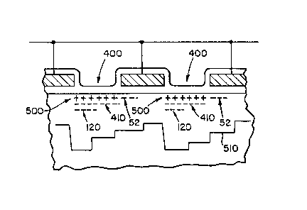
Once the proper edge alignment ha6 been
achieved ~or the first set of implant s~rips and ~heir
reSpective overlying electrodes, a virtual-phase elec-
~rode construction is possible 3 using only the first set
of thus-formed electrodes. This is accompllshed by
picking up the process as it is completed as shown at
Fig. 2J, and by the following addltional BtepS: l) ion
implanting through the entire exposed groove 400, Fig.
2J, strips 410 of acceptor dopants such as boron that
extend the full width of grooveæ 400, Fig. 3. 2~ This
is then followed by an optional heating step, for
example, at 950C for 30 minutes, which diffuses strip6
120 and 410 deeper into the substra~e. 3~ Thereafter,
a final strip 500 o~ donor dopant 6uch as arsenic i~
implan~ed through grooves 400. The result i8 the series
of stepped potential wells schematically indicated by
line 510.
As noted Above, ~he process can be used to
edge-align an lmplanted barrier used to crea~e a lateral
overflow drain. Such a structure is shown in Fig. 4.
Portion 600 of the substrate 610 is the implan~ed drain,
connected to a voltage source not shown. Layer 620 is
an isolat~on oxide layer, and elevated ri~ge 630 seen in
the background is the oxide-cos~ed polysilicon strip
comprising one of the CCD electrode6. The afore-
described process is effective ~n edge-aligning edge 632
of implant barrier 600, wi~h edge 634 of the polysilicon
strip. The implant so created is schematically shown as
dashed line 640 "within" the substrate.
Still another alternative to using tail por-
tions 34 is shown ln Fig. 5. This embodiment is par-
ticularly useful if the process minimi~es subsequent
heatlng as would cause lateral diffusion of the
implanted dopant strip. Parts similar to those
.~ 62'~ 0
-12-
previously described bear the ~ame reference numeral~ to
which the distinguishing suffix "a" is appended. Thus,
a layer 14a of polysilicon i8 provided w~th ~trip~ 20a~
as before. A multil~yer re~ist ma~k is then used,
comprising a planarizing layer 640, a barrier layer 650
6uch as a spun-on-glass, and a relatively thin
photoresist layer 660, as iB conventional in such a
mask. By exposing ~nd developing firgt layer 660 flnd
etching layer 650, layer 640 can be anisotropically
etched to produce the results of Fig. 5. The re~t of
the processing follows the procedures of the previou6
embodiment, uGing the appropriate etchant6 for ~trip
removal 6 .
Ye~ snother method iB available or forming
strips 70 of poly~ilicon that are edge-aligned with the
implanted dopant strips therebelow. This method is
illustrated in Fig~. 6-8. Part~ ~imilar to those pre-
viouæly de~cribed bear the same reference numeral ~o
which the distinguishing suffix "b" is appended. Thi~
method starts out with the same steps as in Figs. 2A-2C
of the previous embodiment, except that layer 14b ~s a
very thin layer (lOOOA or less) of sllicon, for
exsmple, amorphou~ silicon, for~ed on oxide layer 12b,
and strips 20b are preferably all Si3N4. At thls
2S polnt, strips 700 of polysilicon or amorphous silicon
are deposited on the layers 12b and 14b exposed between
strips 20b. Most importantly, these strips have a
thickness sufficient to survive the etching discussed
below. Preferential deposition of silicon at these
loeations and not on the Si3N4 is obtainable by
vapor depositlng the silicon from SiC14 ~ H2 at a
pressure of about 1/100 bar. The fiilicon as deposited
can be alr~ady doped, or doping can be ~chieved by ion
implantation. Thereafter, strips 20b are selectively
etched o, Fig. 7. At this point, the portions of
layer 14b exposed between strips 700 is etched away us-
ing plasma or reac~ive ion etching. Because strips 700
.2 Ei2~ LO
-13-
~re of sufflcient thickness compared to ].ayer 14b, the
result of this etching step is that only the dotted
portion of strips 700, Flg. 8, i~ removed.
Thereafter, the processes of the previously
described embodiment are useful to complete ~he CCD.
Alternativelyg if strips 20b comprise SiO2
and are thick enough for a lift-off pro~ess, the silicon
strips 700 can be deposited both on and between 8trip8
20b (no~ shown), and the portions on strip 20b are
removed when ~he strips 20b are etched away.
Rxample
The following example further illustrates the
scope of the invention.
In accordance with the procedure shown in Figs.
~A-2D, strips 16 of Si3N4, having a thickness of
500A were formed on a 3500A polysilicon layer 14.
Thereafter strips 18 of SiO2, at a thickne~s of
S000~, were deposited. These were then etched through
a mask, us~ng reactive ion etching, to form strips 20,
and then covered with an overall layer 30 of deposited
SiO2 having a thickness of 5000A. Layer 30 was
reactive-ion e~ched through a photoresist mask exposed
and developed as discussed above, to leave tail portions
34. Dopant implantation featured boron using 200 keV of
energy and an expos~re gap between oxide strip~ 32 of 3
~m. The deposited oxide layers were then removed
using a buffered HF etchant, leaving behind the thin
Si3N4 strips. Etchant-resistant strips 60 were
formed by oxidizing ~he polysllicon left exposed by the
buffered HF etchan~. Thereafter, nitride strips 16 were
removed by phosphoric acid at 150C, for 30 mln, and the
exposed polysilicon str~ps were etched using an SF6-
containing plasma etching process.
For compara~ive purposes, the process of Figs.
2A-2F of U.S. Patent No. 4,035,906 was cnrried out to
produce a CCD 8 imilnr to that produced above. That is,
~L~62~
several 25 ohm-cm p-type wafers were processed through
standard gettering and channel stop procedures. There-
after, phosphoruQ was impl~nted blanketwise at a co~cen-
tration of 1.~ X 1012 cm~ 2, by a 150 keV lon implant
to form a buried channel structure.
A layer of silicon dioxide of lOOOA thickn 88
was ~hen grown at 950C in a wet ambient atmosphere. A
layer of photoresist was depo6~ted over this, and
patterned. Arsenlc was implanted into the oxide through
the openings of ~he re~ist, using ion energy of 80 keV
to implant a concentratlon of 1.3 X 1013 cm~ 2 ~
duplicating the condition of Fig. 2B of U.S. Patent No.
4,035,906. The strips of photoresist were then removed.
Next, a layer of polysilicon was deposited
overall, at 62QC, and phosphorus doped at 900C for 30
mlnu~es. This polysilicon layer was then p~tterned o
form a structure es~en~ially duplicative of that of Fig.
2C of U.S. Patent No. 4,035,906.
Thereafter, the layer of oxide between the
polysilicon strips was etched, to remove the As implant
between polysilicon strips. Following the etch step,
isolation oxide was formed and the remaining As implant
caused to diffuse into the substrate. This was achieved
by heating the wafers at 950C for 20 min ln a wet
ambient atmosphere, to duplic~te the conditions shown as
Fig. 2D of U.S. 4,035,906.
Finally, the second phase electrodes were made
as described in U.S. Patent 4,035,906, and a final
anneal at 1050C for 30 min served to further drive the
As into the substrate.
The presence or absence of undesired trapping
wells was then determined both for the above example of
the invention &nd the comp~rative example, by the
following procedure:
At ga~e voltages o 0 volts, the potential well
in the phase 1 storage region of the comparison waers
was ound to be 12.8 eV. In the phase 1 transfer
region, the potentiAl was 5.2 eV. Most lmportantly, at
the boundary between the phase 1 storage region and the
phase 2 transfer region, there was a well that Wa8
approximately 3 eV deep and 1 ~m wide. This latter
produced poor charge transfer efficlency.
In contras~, the above-noted Example of this
inven~ion wae found to have no such boundary well
between the phase 1 s~orage region and the phage 2
transfer region or between the phase 1 transfer region
and phase 2 storage region.
The invention has been described in detail with
par~icular reference to preferred embodlments thereof,
but it will be understood that variations and modifica-
tions can be effected within the spirit and scope o ~he
invention.