Note: Descriptions are shown in the official language in which they were submitted.
Titles "R~diation Detector Module"
DISCLOSURE
The invention herein disclosed relates generally to radihtion
detection ~nd flcguisition systems having wide applications including, inter
alia, parts presence dctermination, process control, thickness ~uging,
moisture content analysis and radiation level detection such as in the
vicinity of nuclear reactor chambers. More particularly, the invention
relates to R radiation detector module for use in such systems.
BACKGROUND
Radiation detection and acquisition systems have had many
applications. Many such systems are characterized by a radiation detector
probe employed at ~ radifltion detection site and electrically coupled to a
probe output si~nal processing unit commonly referred to as a nuclear
instrumentation module. One common type of detector probe is based on a
scintillator crystal combined with a photomultiplier tube. The scintillator
crystal converts impinging invisible rædiation to bursts of visible light which
are converted by the photomultipLier tube to electrical analog signQls. The
radiation involved may be gamma rays, X-rays, high energy or thermal
neutrons, etc.
2 ~ Heretofore, the scintillator crystal and photomultipli~r tube
were packaged in ll common housing for positioning and mounting at the
detection site. The analog output of the photomultiplier tube would be line
coupled to the usually remotely located nuclear instrumentation module
which processed the analog output of the photomultiplier tube so as to
provide, for example, pulse count data to an associated display or system
controller.
One problem with this prior system was that the nuclear
instrumentation module had to be located relatively close to ttle detector
probe to avoid loss of signal integrity resulting from induced line noise, line
losses, etc. Also, the nuclear instrumentation modules could not be used
uni~rersally with different detector probes operative to sense respective
types of rediation. Instead, a specific instrumentation module had to be
--2--
used for each radiation type detector probe. Moreover, the output of such
system was not as reproduceable or repeatable as might be desired in some
~pplications le~ding to larger margins of error or reduced reliability.
Still another problem was the variance in outputs from detector
probe to detector probe. This necessitated tedious and time consuming
calibration of the nuclear instrumentation modùles to gain matching data
output under identical radiation conditions. Many times d good match could
not be obtained because of substantial variance in the detector probes and
calibration limitations of the nuclear instrumentation modules.
Such systems also required a separate nuclear instrumentation
module for each detector probe in multiple channel systems. In flddition to
being costly, large control panels were required to house the nuclear
instrumentation modules and associated equipment such as pulse count rate
displaysO
RELATED APPLICATION
~ co~ending U.S, Patent Application Serial No. 637,434J filed
August 3, 1984 ~nd entitled "Radistion Detection and Acquisition System",
there is disclosed ~ r~diation detector probe or module and associated
acquisition system which eliminates or minimizes the afores~id and other
2 problems, and whiah has a wide range of applications. The radiation
detector module is characterized by the integration in a compact package of
scintillator probe and ~upporting electronics which provide digital pul~e
count signals in response to detected seintillations that may be transmitted
by a differential line driver on twisted shielded wire pairs over great
distances, as on the order of several thousand feet, to a count signal
processing unit while maintaining signal integrity. The digital pulse count
output is independent of the type of radiation detected, i.e., gamma raysl X-
rays, thermal neutrons, etc., whereby the same count signal processing unit
mfly be employed w;th different detectors for respective different radi-
3 0 ations. The same electronics are employed in the detector probe for
different radiations and radiation energies through analog gain adjustment
of the scintillator probe output. The detector module may also have an
~nalog signal OUtpllt so that it may be interfaced to an anfllog signal
3-
analyzer such as a conventional nuclear instrumentation module. A third
output of the detector module provides a digital output signal that reflects
saturation of the electronics due to a high rate o detected scintillation
events (pulse pile-up). The persistence of this pulse pile-up signal for
periods greater than a preselected time period such as one millisecond may
be related to the occurrence of a criticality condition.
A single, remotely located, rnicroprocessor~ased si~nnl pro-
cessing unit also is provided to acquire count signals receSved on multiple
channels from respective detector probes, to display such dat~ and to
transmit such data to ~ controller or monitor for process control and/or
monitoring. Acquisition is effected Yia at least one detector/processor
interface tnodule having plural tr~nsmission line inputs for connection to
respective detection modules and a common transmission line output for
connection of said inputs to the signal processing unit.
More particularly, the radiation detector module includes a
scintillator for receiving radiation to be detected and for emitting scintilla-
tion light in response to received radiation, a photoelectric transducer
optically coupled to the scintillator for generating electrical analog output
sign~ls in response to detected scintillations, n low level discriminator foP
2Q genersting pulse count signals in response to analog output signals exceeding
a threshold level, and a differential line driver for digitally transrnitting ~he
pulse output signals to a remotely located differential line receiver ~g m~y
be associate.d with a slgnal processing unit. The low level discrimin~tor may
be set to prevent a pulse count signal from being generated at the output of
the detector in response to detected scintillations caused by incident
radifltion having an energy level below a specified value or lower limit.
Acoordingly~ scintillations produced by low energy background radiation or
low energy radi~tion caused by secondary reaotions in the scintillator msy
be excluded from the count.
l[n some applications, it also would be desirable to exclude from
the pulse count output of a detector those scintillations produced by
incident radiation having an energy level above a specified upper limit ~s
well as those scintillations produced by incident radiat;on below a specified
19~
lower limit. That is, only those scintillations caused by incident radi~tion
having an energy level f~lling between the upper and lower limits would
result in a pulse count signal being generated at the output of the detector~
E}y way o~ example, a r~diation detector may be used for ~uging
of sheet metal. The sheet metal to be gauged is passed or placed between a
source of radiation and the radistion detector such that the detector will be
located in the shadow of the sheet met~l. The radiation emitted by the
source thereof will theP~ have to pass through the sheet metal in order to
produce a scintillation at the front end of the detector. lf the radiati >n is
of a type that will be attenuated as a function of sheet metal thickness, the
rate ~t which scintillations are produced in the detector by such radiation
will ~lso be a function of sheet metal thickness. If only the sc;ntillation~
c~used by the attenuated radi~tion result in pulse count signals at the output
of the detector, the r~te of such pulse count output signals likewise would
be H function of metal thickness - the hi~her the rnte, the thinner the
material.
The radiation source, however, may c~use plural radiation in-
duced pealcs in the scintillator which correspond to different energy leveJs
of incident radiation. The low energy radiation may be attenuated by the
sheet metsl as discussed sbove but the high energy radiation might pass
essentially freely through the sheet metal and not be attenuated. Accord-
ingly, the high energy r&diation which is nvt sttenuated will produce
s~intillations in the detector at a rate independent of the thickness of the
sheet metal. It would be desirable th~t the scintillations produceà by the
high energy r~diation not result in pulse count signals at the output o~ the
detector while the scintillations produced by the low ener~y (attenuated)
rsdi~ion result in pulse count output signsls at a r~te proportionally related
to the thickness of the sheet metal.
Of course there may be other applications wherein radiatîon
events associated with high energy radiation desirably are not to be included
in the pulse count output o~ Q detector. ~loreover, it would be highly
desirable to provide for high level ~s well ~s low level discriminfltion in
comp~ct detector module ~e.pable of transmitting its pulse count output
--5--
digitally over relatively long dlstances. Further, it would be desirable to
elimin~te the need for a high voltage supply line leading to a detector
utili~ing a photomultiplier tube ss its photo-electric $rans;3ucer.
SUMMARY OF THE INVENTION
The present invention provides a novel radiation detector probe
or module characterized by the integration in a compact package o~ a
scinti~lator probe and suppor$ing electronics hav;ng provision for high and
low level discrimination. The radiation detector module may be set to
provide digital pulse count signals in response to detected scintillations
produced by only that radiation falling within an energy window, i.eO,
between upper and lower radiation energy limits, for selective radiation
detection.
More particularly, the radiation detector module includes a
scintil~ator for receivinK radiation to be detected ~nd for emitting scintilla-
tion light in response to received radiation, a photo-electric transducer
optically coupled to the scintillator for generating electrical analog output
signals in response to detected scintillations, a discriminator for generating
pulse count signals in response to analog output signals falling between
lower and upper threshoid levels, and a differential line driver for digitally
tr~nsmitting the pulse output si~nals to a remotely located differenti~l line
receiver. Provision is made for base line adjustment of the analog output of
the transducer and the discriminator includes high speed lower ~nd upper
comparators and associsted logic circuitry for generating ~ pulse count
signal in response to a pulse produced by the lower limi~ comparator only
when no corresponding pulse is produced by the upper limit comparator.
Further in accordance with the invention, the photo-electric
trensducer may include a photomultiplier tube powered by a high voltage
power supply integrally included in the radiation detector module. Provision
also is made for mechnnically decoupling the photomultiplier tube ~or
3 o vibration ~nd shock resistance.
To the accomplishment of the forego;ng and related ends, the
invention, then) comprises the features hereinafter fully described and
particularly pointed out in the claims, the following description and the
--6--
allnexed drawings s~tting forth in detail a certnin illustrative embodi~nent of
the invention, this being indicative, however, of but one of the various ways
in which the principles of the invention may be employed.
BRIEF DESCRIPTION OF THE DRAWINGS
In the annexed drawings:
Fig. 1 is a perspective view, partly broken away, of a radiation
detection rnodule according to the invention;
Fig. 2 is a diagrammatic illustration of the radiation detection
module;
Figs. 3 and 4 are circuit schernatics of the electronics illustrated
in Fig. 2; and
Fig. 5 is a fragmentary cross-section taken substantially along
the line 5-5 of Fig. 1.
DETAILED DE~SCRIPTION
Referring now in detail to the drawings and initially to Fig. 1, a
radiation detector module according to the invention is designated generally
~y. reference numeral 10. The radiation detection module 10 generally
comprises a scintillator probe or detector front end 11 integrated with
supporting electronics 12 in a single housing 13. The housing 13, a~ will be
2 0 appreciated, may be quite compact.
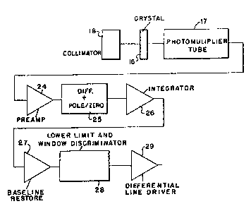
As is depicted in Fig. ~, the scintillator probe 11 includes a
scintiLlation element 16 optically coupled to a photo-electric transducer 17.
The scintillation element may be A scintillation crystal such as one sold
under the trademarlc POLYSCIN by the Harshaw/Filtrol Partnership o
Cleveland, Ohso, and the transducer may be a photomultiplier tube of
suitable type. By w~y of example~ the crystal may be a 1.0 inch diameter,
1/4 inch thick disc optically coupled to the face of a 1.0 inch diameter
photomultiplier tube. There may also be provided e, collima~or 18 flnd as
best seen in Fig. 1, the crystal, photomultiplier tube and collimator
3 o preferably are hermetically sealed in an aluminum cylinder 18 which
provides the necessary electrostatic shielding. As discussed in greater
detail below, the scintillator probe is mounted in the housing 13 but
mechanically decoupled at both ends for vibration resistance. There may
--7--
also be mounted in the housing a high voltage power supply 19 for powering
the photomultiplier tube. The power supply preferably is a miniature
DC-DC converter which is adjustable to deliver between 500-1000 volts to
the high voltage terminals of the photomultiplier tube from a 15 volt
battery. Such a power supply i5 available from Bertan. The provision of an
internal high voltage power supply eliminates the need for ~n external high
voltage power supply line and connection which may create a potential
hazard in explosive detector environments.
In Fig. 29 the electronics or electronic circuitry 12 is also dia-
grammatically illustrated. The circuitry 12 generally cornpr;ses a low noise
charge sensitive pre-amplifier 24~ a differentiator 25 with ~ pole/zero
adjust, a pulse shaper amplifier 26, a base line restore 27, fl lower limit and
window discriminator 28, and a differential line driver 29 for transmitting
digital pulse count data. Low voltage electric power may be provided from
a conventional power supply, as to convention~l filtered input regulators 30-
32 (if necess~ry or desired) as seen in Fig. 3.
Referring now to the circuit sehematic seen in Figs. 3 and 4, the
output of the photomultiplier tube 17 applied to input terminal 33 is AC
coupled by input capacitor 34 to the input of the low noise charge sensitive
pre-amp` 24. Also provided is a diode clipping c;rcuit 35 which protects the
input circuitry illustr~ted from excessively large signals coming from the
photomultiplier tube. If desired, a test input tlerminal 36 m~y be provided
~nd connected by an RC circuit 37 to the inverting input 38 of the pre-amp
24.
As light is produced in the scintillation crystal 16, such light
impinges on the photomultiplier tube 17 causing the same to output a charge
pulse via terminal 33 and capacitor 34 to the charge sensitive operational
amplifier 40 of the pre-amp ~4 to produce on line 41 an amplified pulse
proportionately representative of the intensity of light impinging on the
photomultiplier tube. The response time of the pre-amp a4 may be less than
one microsecond, with a decay time ¢onstant of lS microseconds; these
values, of course, are exemplary only and others could be employed by
altering the various components used in the circuitry.
~t~ 3~
The output of the pre-amp 24 on line 41 is delivered by the
differentiator 25 to the pulse shaper amplifier or integrator 26. The
differentiator 25 is an RC differentiation circuit and the decay time o~ such
circuit is set by capacitor 44 and the resistance vnlue of an adjusting
potentiometer ~5 which is adjustable for pole/zero compensation.
The pulse shaper amplifier 26 may include one or more conven-
tional low pass filter stages although only one is shown. The parsllel
connected, feed~ack capacitor 46 and resistors 47 and 48 across the
operational amplifier 49 determine the cut~ff frequency of the pulse shaper
amplifier 26, and the capacitor 50 is provided for damping. The capacitor
50 decreases the rise time of the pulse signal and produces a more
symmetrical wave shape. The output of the pulse shaper amplifier 26 will
be a subst~qntially symmetric~1 wave shs~pe with an amplitude of say 5 volts
for the incident radiation peak energy adjusted by controlling the value o
the operAting high voltage supplied to the photomultiplier tube by the
intern~l high voltage power supply 19. This gain adjust permits the
scilltill~tion probe 11 to be matched to a specific radiation source, i.e., to fix
~t a specified amplitude, say 5 volts, the analog signal peak height
corresponding to the incident rsdiation pealc energy. The rise ~nd f~ll of the
pulse signsl output of the pulse shaper ~mpliIier 26 should be complete
within 5 microseconds.
As is seen in Fig. 4, the output of the pulse shaper ~mplifier 26
on line 54 is buffered by an amplifier circuit 55 and the buffered output on
line 56 is AC coupled via capacitor 57 to the junction 58 of the base line
restore circuit 27 and the discriminator as. The buffered output on line 56
is also delivered via an RC circuit and impedance matching ampUfier circuit
59 to an analog output S9a to which say a 50 ohm coaxial cable m~ be
connected.
The base line restore circuit 27 includes an operAtional ~mplifier
60 having its negative or inverting input connected to the output of the
shaper amp 26 and to a -12 voltL~ge level via resistor 61. The positive or non-
inverting input of the operational amplifier 60 is connected to d base line
adjusting potentiometer 62 which may be adjusted to vary the DC volt~ge
9-
added to the analog output of the shaper amplifier 26 for adjusting the base
line of such analog output at the junction 58, which also is the input to the
discriminator 28.
The discriminator 28 includes a high speed lower limit com-
parator 66 having its inverting input connected to the junction 58 which
receives the base line adjusted output of the shaper amp 26. The non-
inverting input of the comparator ~6 is connected to ground to provide a
reference voltage level to which the base line adjusted analog output of the
shaper amp is compared. Only when the base line adjusted shaper amp
output exceeds the reference voltage level upon the occurrence of a
scintillation of sufficient energy detected by the photomultiplier tube will a
pulse output be passed by amplifier 69 in the lower limit comparator S6 to
line 70. That is, a squared pulse output is obtained on line 70 when the input
si~nal to the comparator 66 is greater than the reference voltage whereby
pulses generated by low level energy scintillations may be effectively
excluded, i.e., not result in a pulse output on line 70. A feedback resistor 71
is incll~ded to induce hysteresis into the circuit to avoid isolations when the
input signal level passes through the threshold region. A resistor 72 tied to
the +5 volt source is included as shown on the output of the comparator to
2 0 produce a squared pulse output signal of desired amplitude on line 70.
By adjusting the base line ~djusting potentiometer 62, the base
line of the shaper amp 26 analog output at junction 58 m~ be ~djusted
relative to the fixed reference voltage at the positive input of the lower
limit comparator 6B. ln this manner, a low threshold level or lower limit
may be determined. By lowering the bsse line, a higher amplitude pulse at
the negative input ~f the lower limit comparator would be needed to cause a
pulse output on line 70. Conversely, the base line may be raised so that
lower amplitude pulses will result in corresponding pulses on line 70. The
basc lins adjusting potentiometer 62 preferably is adjustable to provide for
low level discrimination from 10 KeV to 100 KeV for Am-241, it again being
noted that the shaper amp 26 analog output is proportionately related to the
intensity of ~ scintillation produced in the scintillation crystal 16 wh~ch in
turn i8 proportlonately r~lated to the energy o~ the radiation callsing the
3~
-10-
scintillation. It also is noted that the time duration of a squared wave pulse
on line 70 will be dependent on the amount of time that the amplitude of the
base line adjusted output of the shaper amp 26 exceeds the reterence
voltsge.
The discriminator 28 also includes a high speed upper limit
comparator 80 having its inverting input 81 connected to receive the base
line adjusted analog output of the shaper amp 26 tat junction 58) and its non-
invèrting input connected to an upper threshold adjusting potentiometer 83.
Only when the base line adjusted shaper amp output exceeds the upper
threshold level determined by the zener diode reference voltage generating
circuit 84 according to the adjustment of the potentiometer 83, upon the
occurrence of e scintillation of sufficient energy detected by the photo-
multiplier tube 17, will a pulse output be passed by operational amplifier 85
to line 86. That is, a squ~red pulse output is obtained on line 36 when the
input signal to the comparator 80 is greater than the upper threshold voltage
determined by fhe circuitry coupled with respect to the potentiometer 83.
A feed-back resistor S7 is included to induce hysteresis into the circuit to
~void isolations when the input signal level passes through the threshold
region. A resistor 88 tied to the +5 volt source is included as shown on the
output of the comparator 80 to produce a sguare wave pulse of desired
voltage on line 86 whenever the input si~nal to the upper limit compar~tor i9
greater than the upper threshold voltage. The time durAtion of the square
wave pulse on line 86 will be dependent on the amount of time thst the
~mplitude o~ the base line adjusted input signsl to the upper l;mit com-
parator 80 exceed~ the upper threshold voltage.
As will be seen, a square wave pulse on Iine 70 will only result in
a TTL compatible pulse output signal on line 90 when no corresponding
square wave pulse is produced on line 86. Accordingly, only those pulses at
the output of the shaper amp 26 having an amplitude greater than the low
threshold level determ;ned by base line adjustment but less than the upper
threshold limit determined by adjustment of the potentiometer 83 will result
in an output si~nal on line 90 connected to the output of the discriminator
28. Since an adjustment of the base line ~djusting potentiometer 62 will
3~
result in a change in the minimum amplitude of A sh~per arnp pulse required
to produce a pulse on lin~ 86, the upper limit comparator actually defines a
range of amplitudes above the low level threshold that will result in a pulse
sign~l on line 86 but no pulse count signal on line 90. If the amplitude of the
shaper amp output falls outside this amplitude r~nge or window, either no
pulses ~ill appear on lines 70 and 86 or a pulse will appear on both lines 70
and 86. These pulses on lines 70 and 86 serve as logic input signals to a logic
circuit 93 which determines whether or not a pulse count signal is to be
produced at the output of the differentiator. The upper threshold Rdjusting
potentiometer 83 preferably is adjustable to provide for upper level dis-
crimination from 10 KeV to 100 KeV.
The logjc circuit 93 includes a one-shot multivibr~tor 94 h~vlng
an AND logic gate 95 at its input. The AND gate 95 has two inputs, one
input connected to the output of the lower limit comparator 66 and an
inverted input connected to ground. As long as the output of the lower limit
comparator remains at logic one, ~s when the amplitude of the base line
adjusted an~log output of the shaper amp 26 is below the reference voltage
input to the lower limit comparator, the AND gate ~5 will maintain ~ logie
one signal at the input of the one-shot multivibrator 94. However, upon
detection of a scintillation exceeding the low threshold level, a logic zero
square wave pu~se will be produced on line 70 and the AND g~te will produce
a logic zero at the input o the one~hot multi~vibr~tor for the duration of
such logic zero p~se. When a logic one signal again is produced an line 70
at the tr~iling end of the pulse produced ~t the output of the lower limit
comparator, the AND gate will again produce a logic one sign~l and trigger
the one-shot multivibrator 94 unless it has been turned off by connection of
it~ inverted clear input to ground via line 96 and ~ flip-flop circuit 100.
When triggered, the one-shot multivibr~tor will produce a TTL compatible
output signal on line 90 for a period determined by the resistor 97 and
3 0 capacitor 98, say 1 microsecond~
The line 96 is connected to the output of the flip-flop circuit 100.
Ench time the flip-flop circuit 100 is reset, R logic low voltage, such as O
volts, i~ produced on line 96 thereby turning on the one-shot multivibr~tor
9~ at its inverted clear input.
- - .
-12-
As shown9 the inverted CLK input of the flip-flop circuit 100 is
connected to the output oI the upper limit comparator 80 by line ~6. As
long as the output of the upper limit comparator remains at logic one, a~
when the Hmplitude of the base line adjusted Hnalog output of the sh~per
amp 26 is below the reference voltage input to the upper limit compar~tor,
the flip-flop will rem~in unchHnged and continue to apply a negative volta~e
on line 96. However, upon detection of a scintillation exceeding the upper
threshold level, a logic zero squ~re wave pulse will be produced on line 86
and the flip-flop will ch~nge its state ~nd connect the line 96 to ground.
10Accordingly, a scintillation exceeding the upper threshold level will turn off the one-shot multivibrator 94.
In the event of a scintillation exceeding the upper threshold
level, both the lower limit and upper limit comparators 66 and 8û will
produce a sgu~re wave pulse respectively on lines 70 and 86. Bec~use of the
~ener~lly symmetrical wave sh~pe of the shaper amp (26~ pulse output, the
pulse produced by the upper limit comparator 30 will begin after and end
sooner than the pulse produced by the low limit comparator 66. Accord-
ingly, the flip-flop circuit mo will have been caused to change state before
the one~hot multivibrator 94 can be triggered at the trailing end of the
20 pulse output signHl OI the low limit comparator 66. As a result of this~ the
one~hot multivibrHtor 94 will not produce a pulse output signnl on line 90.
- If the scintillation exceeds only the lower threshold level, the
lower limit compar~tor 66 will produce a pulse on line 70 but the upper limit
compar~tor 80 will not produce a pulse on line 8B. Accordingly, the nip-nop
circuit 100 will not be caused to change state and the one-shot multivibrator
94 will remain on to produc~ a pulse output signal on line 90. Qf course, no
pulse output signal will be produced on line 90 if the scintillHtion is below
the low ths eshold level.
As is further seen in Fig. ~, there is provided ~nother one-shot
30 multivibrator 104 having an AND logic gHte lOS at its illpUt. The AND gate
lOS has two inputs, one input connected to the output of the lower limit
comparator 66 and an inverted input oonnected to ground. As lon~ HS the
output of the low~r limit comparator remains at logic one, the AND ~ate
. ~_ , .
-13-
will maintain a logic one signal at the input of the one~hot multivibrator
104. However, upon detection of a scintillation exceeding the low threshold
level, the logic zero square wave pulse produced on line 70 will cause the
AND gate 105 to produce a log~c zero at the input of the one-shot
multivibrator 104 for the duration of such logic zero pulse. When a logJic one
signal again is produced on line 70 at the trailing end of the logic zero pulse
produced at the output of the lower limit comparator 66, the AND gate 105
will again produce a logic one signal and trigger the one-shot multiYibrator
104. When triggered, the one~hot multivibrator 104 wi~l supply a negative
going voltage pulse signal via an RC circuit 107 to the inverted clear input
of the flip~flop circuit 100 to reset such flip-nop circu;t. The RC circuit 107
factors in a time delay of say 40 nanoseconds to prevent premature
resetting of the flip-flop c;rcuit. Regardless of its prior stste, the flip-flopcircuit when reset will then eause a logic low voltage to be applied to the
inverted clear input of the one-shot multivibrfltor 94.
The output of the differentiator 28 is inputted via line 90 to the
difîerential line driver 29 which preferably is an RS~22 balanced differerl-
tial line driver which digitally transmits the pulse count signals receiv~d
from the discriminator. The differential line driver has two logic gates, one
an AND gate 110, and one a NAND gate 111. The illustrated connections in
Fig. 4 provide three OI the inputs to each of the gate~ with a +5 volta~e
level signal and one input to each of those gates is connected to line 90 to
receive the TTL compatible signal output from the discriminator. Accord-
ingly, when there is a logic one signal on line 90, for example upon
occurrence of a scintillation detected by the radiation detection module
falling between the upper and lower threshold levels (within the energy
window), the AND gate 110 will produce a logic one signal on its output line
lla, and the NAND gate 111 will produce a logic ~ero signal on its output line
113. Similarly, when a zero signal is spplied on line 90, the AND gate
produces a logic zero signal at its output and the NAND gate produces a
logic one signal at its output.
Since the outputs oî lines 112 and 113 always are opposite each
other, signal integrity with minimum loss is possible for transmission o~ler
-14-
rclatiYely long distances of, for example, 3,000 feet. The udvantage to such
lengthy transmission is the abi1ity to Iocate, for example, a single signal
processing unit (including a receiver operated in b~l~nced configuration with
the driver) at a remote location from the radiation detection module 10.
The signal processing unit may conveniently monitor many radiation detec-
tion modules at respective remote locations~ For further details respecting
a preferred signal processing un;t and assoc;ated components such as ~
detectorJprocessor interface module, reference m~ be had to Canadian Patent
~p~Iication Serial No. 482,733, filed May 29, 1985 and entitled "Radiation
Detection and Accumulation System". The herein disclosed radiation
detector module may be substituted for detector disclosed in such ~pplica-
tion in the overall detect;on end accumulat;on system.
~ s will be appreciated, the scintillator probe 11 of the herein
disclosed radiation detector module 10 may take other forms than the illus-
trated probe utilizing ~ photomultiplier tube. For example, the scintillator
probe may compr;se a scintillation crystel optically coupled to a photodiode
as in the manner described in the above-referenced application wh;ch is
hereby fully incorporated herein by reference.
Referring now $o Figs. 1 and 5, the housing 13 includes a frame
consisting of four parallel rails 120 secured to 8 rectangular support block 121dt respecti~e corners of the lstter. The support block 121 is located
intermediate the lengths of the rails which extend between opposite ends of
the housing. A~ each end of the housing, a respective front and rear end
plate 122, 123 is secured to the ends of the bars with a housing cover 124
trapped therebetween. The SLIpport block 121 ;s spaced from the front end
plate 122 by a distance approximately equal the length of the scintillator
probe 11.
As seen in Fi~. 5~ the front end plate 122 includes a bore 126
aligned with the front end of the scintillator probe 11. At the inner side o~
the front end platet there is provided a cylindrical counterbore 12~ sized to
receive an O-r;ng 12~ closely circumscrib;ng the scintillator probe. The O-
ring 128 is retained between an annular flange 129 on the scintillator probe
caslng 18 and the bottom of the cylindrical counterbore 127. A similar but
,~
--15--
oppositely disposed arrangement is provided at the support block 121. That
is, the support block has a circular bore through which the scintillator probe
extends andt at its side facing the front end plate, a cylindrical counterbore
for receiving an O-ring gasket retained between the bottom of the counter-
bore and an annular flange on the scintillator probe casing. When the front
end plate is secured to the ends of the rails by screws, the front end plate
and support block will firmly yet resiliently hold therebetween the scin-
tillator probe. With this arrangement, the scintillator probe is mechanically
decoupled for vibration resistance by reason of the O-rings which resiliently
hold the probe in the housing. As a result, the detector mRy withstand high
g forces such as lU g's or even as high as 20 g's without damage to the
scintillator probe.
Although the invention has been shown and described with
respect to a preferred embodiment, it is obvious that equivalent alterations
and modiications will occur to others skilled in the art upon the reading and
understanding of the specification. The present invention includes all such
~quiv~lent alterations and modifications, and is Limited only by the scope of
the following claims.